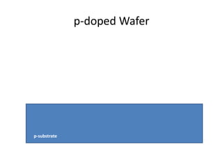
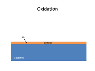
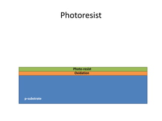
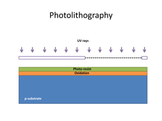
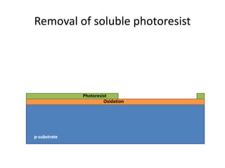
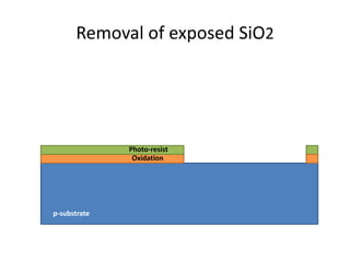
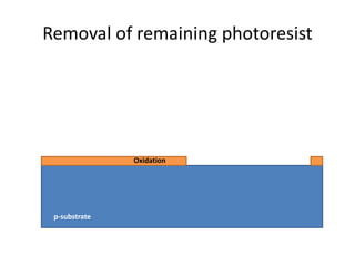
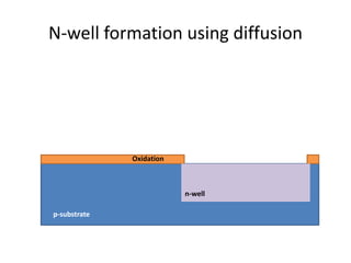
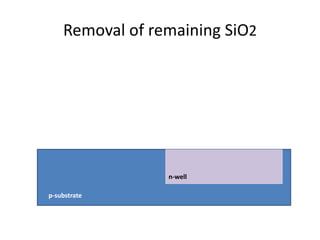
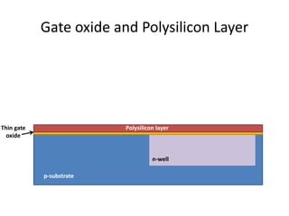
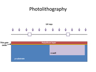
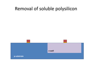
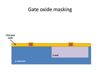
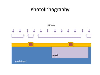
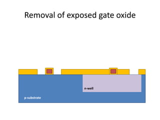
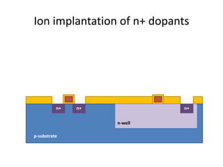
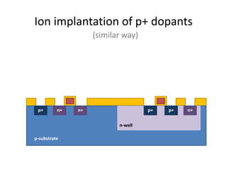
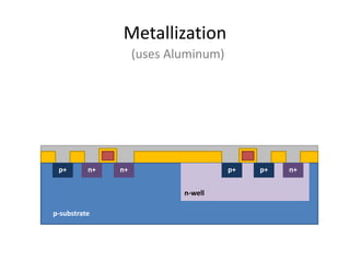
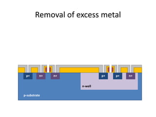
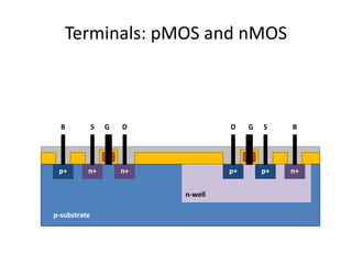
The document details the CMOS fabrication process, specifically focusing on the n-well process on a p-doped wafer. It outlines several steps including oxidation, photolithography, ion implantation, and metallization, leading to the creation of n+ and p+ terminals for PMOS and NMOS. Each step is described in relation to the removal and application of materials and layers involved in the process.