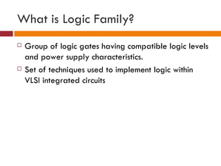
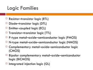
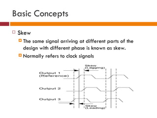
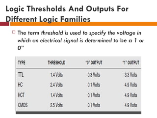
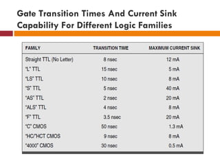
DIGITAL IC
What is Logic Family?
   Group of logic gates having compatible logic levels
    and power supply characteristics.
   Set of techniques used to implement logic within
    VLSI integrated circuits
Logic Families
   Resistor–transistor logic (RTL)
   Diode–transistor logic (DTL)
   Emitter-coupled logic (ECL)
   Transistor–transistor logic (TTL)
   P-type metal–oxide–semiconductor logic (PMOS)
   N-type metal–oxide–semiconductor logic (NMOS)
   Complementary metal–oxide–semiconductor logic
    (CMOS)
   Bipolar complementary metal–oxide–semiconductor
    logic (BiCMOS)
   Integrated injection logic (I2L)
Basic Concepts
   Fan In: Maximum no. of inputs of gate
     Increase   in fan in increases gate delay
   Fan out: Maximum no. of outputs gate can drive
     The  fan-out really depends on the amount of electric
      current a gate can source or sink while driving other
      gates.
     Increase in fan out can affect noise margin, operating
      temperature, rise time, fall time and propagation
      delay.
Basic Concepts
   Gate delay
     Delay   offered by a gate for the signal appearing at
      its input, before it reaches the gate output.
     Also known as propagation delay.

   Wire Delay
     Delay  offered by interconnection between gates
     Also known as interconnect delay
Basic Concepts
   Skew
     The same signal arriving at different parts of the
      design with different phase is known as skew.
     Normally refers to clock signals
Basic Concepts
   Logic levels
     VOHmin : The minimum output voltage in HIGH state (logic
      '1'). VOHmin is 2.4 V for TTL and 4.9 V for CMOS.
     VOLmax : The maximum output voltage in LOW state (logic
      '0'). VOLmax is 0.4 V for TTL and 0.1 V for CMOS.
     VIHmin : The minimum input voltage guaranteed to be
      recognised as logic 1. VIHmin is 2 V for TTL and 3.5 V for
      CMOS.
     VILmax : The maximum input voltage guaranteed to be
      recognised as logic 0. VILmax is 0.8 V for TTL and 1.5 V for
      CMOS.
Basic Concepts
   Current levels
       Source and sink capability
   Noise Margin
     Low noise margin (LNM) = VILmax-VOLmax
     High noise margin (HNM) = VOHmin-VIHmin
   Rise time (tr)
   Fall time (tf)
   Propogation delay (tpd)
       The time between the logic transition on an input and the
        corresponding logic transition on the output of the logic
        gate.
Basic Concepts
   Power dissipation
     Static
           power dissipation
     Dynamic power dissipation
Logic Thresholds And Outputs For
Different Logic Families
    The term threshold is used to specify the voltage in
     which an electrical signal is determined to be a 1 or
     0”
Gate Transition Times And Current Sink
Capability For Different Logic Families
Practical digital signal
Thank You

Basics of digital ic

  • 1.
  • 2.
    What is LogicFamily?  Group of logic gates having compatible logic levels and power supply characteristics.  Set of techniques used to implement logic within VLSI integrated circuits
  • 3.
    Logic Families  Resistor–transistor logic (RTL)  Diode–transistor logic (DTL)  Emitter-coupled logic (ECL)  Transistor–transistor logic (TTL)  P-type metal–oxide–semiconductor logic (PMOS)  N-type metal–oxide–semiconductor logic (NMOS)  Complementary metal–oxide–semiconductor logic (CMOS)  Bipolar complementary metal–oxide–semiconductor logic (BiCMOS)  Integrated injection logic (I2L)
  • 4.
    Basic Concepts  Fan In: Maximum no. of inputs of gate  Increase in fan in increases gate delay  Fan out: Maximum no. of outputs gate can drive  The fan-out really depends on the amount of electric current a gate can source or sink while driving other gates.  Increase in fan out can affect noise margin, operating temperature, rise time, fall time and propagation delay.
  • 5.
    Basic Concepts  Gate delay  Delay offered by a gate for the signal appearing at its input, before it reaches the gate output.  Also known as propagation delay.  Wire Delay  Delay offered by interconnection between gates  Also known as interconnect delay
  • 6.
    Basic Concepts  Skew  The same signal arriving at different parts of the design with different phase is known as skew.  Normally refers to clock signals
  • 7.
    Basic Concepts  Logic levels  VOHmin : The minimum output voltage in HIGH state (logic '1'). VOHmin is 2.4 V for TTL and 4.9 V for CMOS.  VOLmax : The maximum output voltage in LOW state (logic '0'). VOLmax is 0.4 V for TTL and 0.1 V for CMOS.  VIHmin : The minimum input voltage guaranteed to be recognised as logic 1. VIHmin is 2 V for TTL and 3.5 V for CMOS.  VILmax : The maximum input voltage guaranteed to be recognised as logic 0. VILmax is 0.8 V for TTL and 1.5 V for CMOS.
  • 8.
    Basic Concepts  Current levels  Source and sink capability  Noise Margin  Low noise margin (LNM) = VILmax-VOLmax  High noise margin (HNM) = VOHmin-VIHmin  Rise time (tr)  Fall time (tf)  Propogation delay (tpd)  The time between the logic transition on an input and the corresponding logic transition on the output of the logic gate.
  • 9.
    Basic Concepts  Power dissipation  Static power dissipation  Dynamic power dissipation
  • 10.
    Logic Thresholds AndOutputs For Different Logic Families  The term threshold is used to specify the voltage in which an electrical signal is determined to be a 1 or 0”
  • 11.
    Gate Transition TimesAnd Current Sink Capability For Different Logic Families
  • 12.
  • 13.

Editor's Notes

  • #11 TTL = Transistor Transistor Logic, HC / HCT stands for High-speed CMOS Logic (HCL)