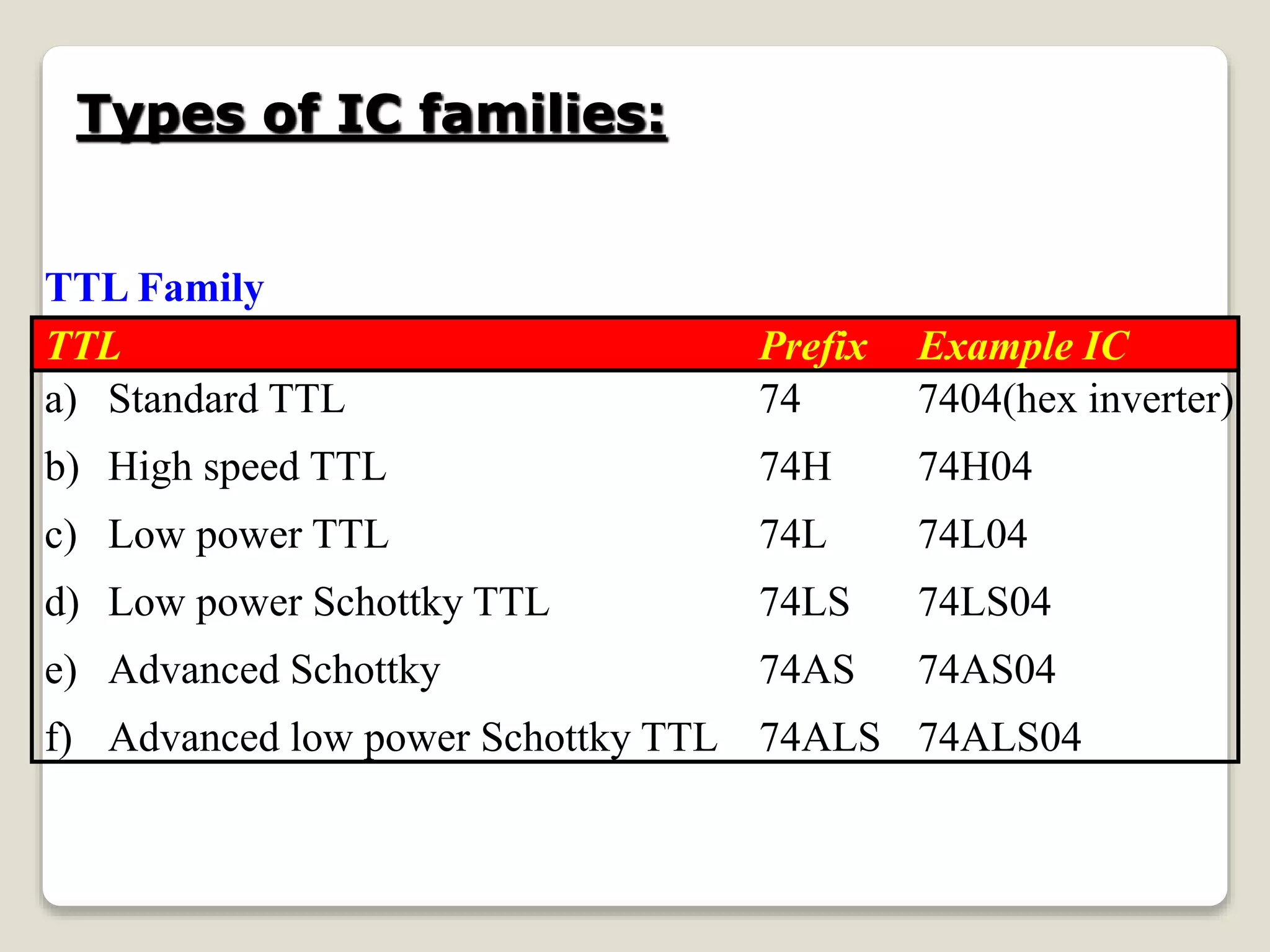
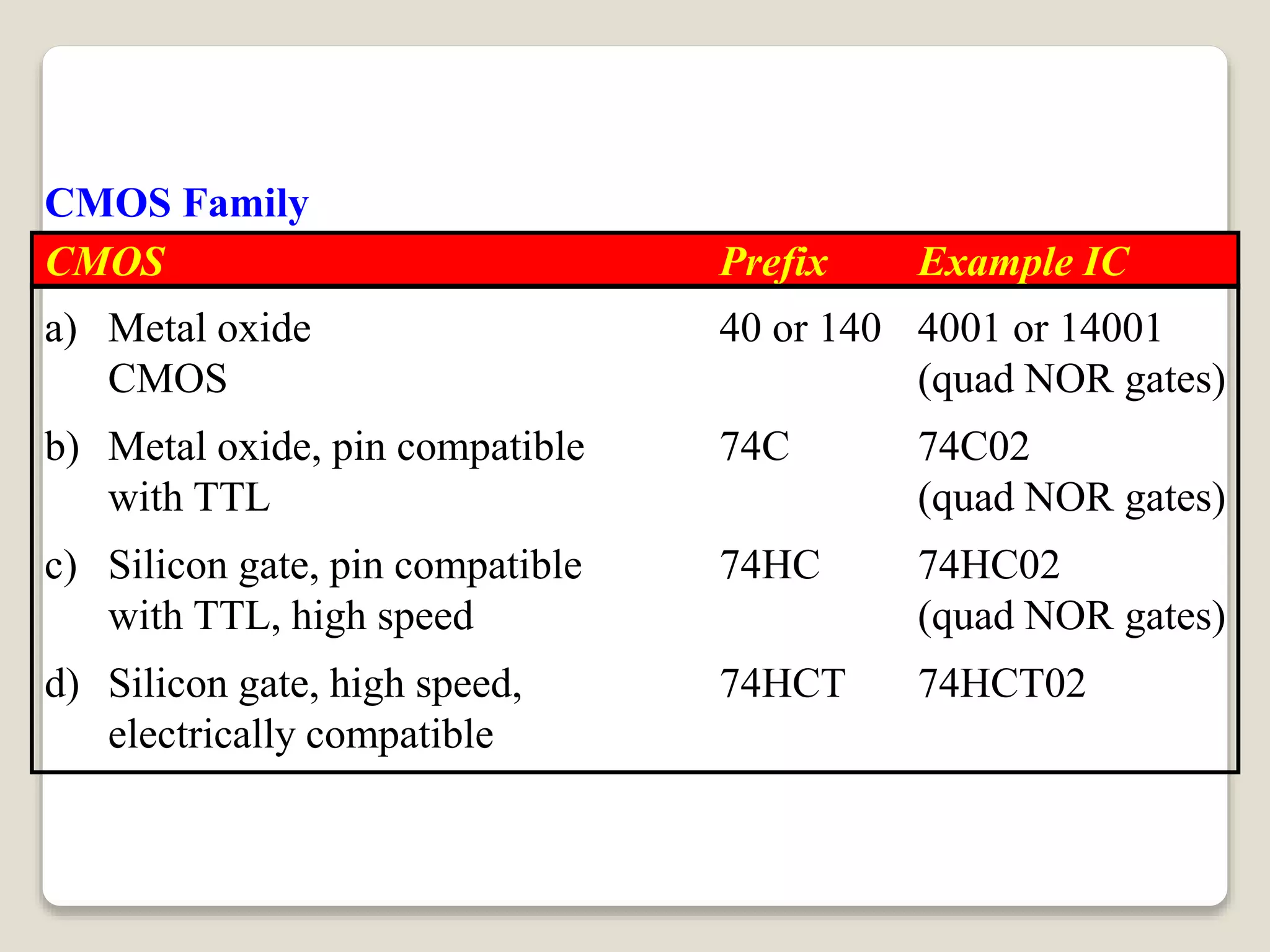
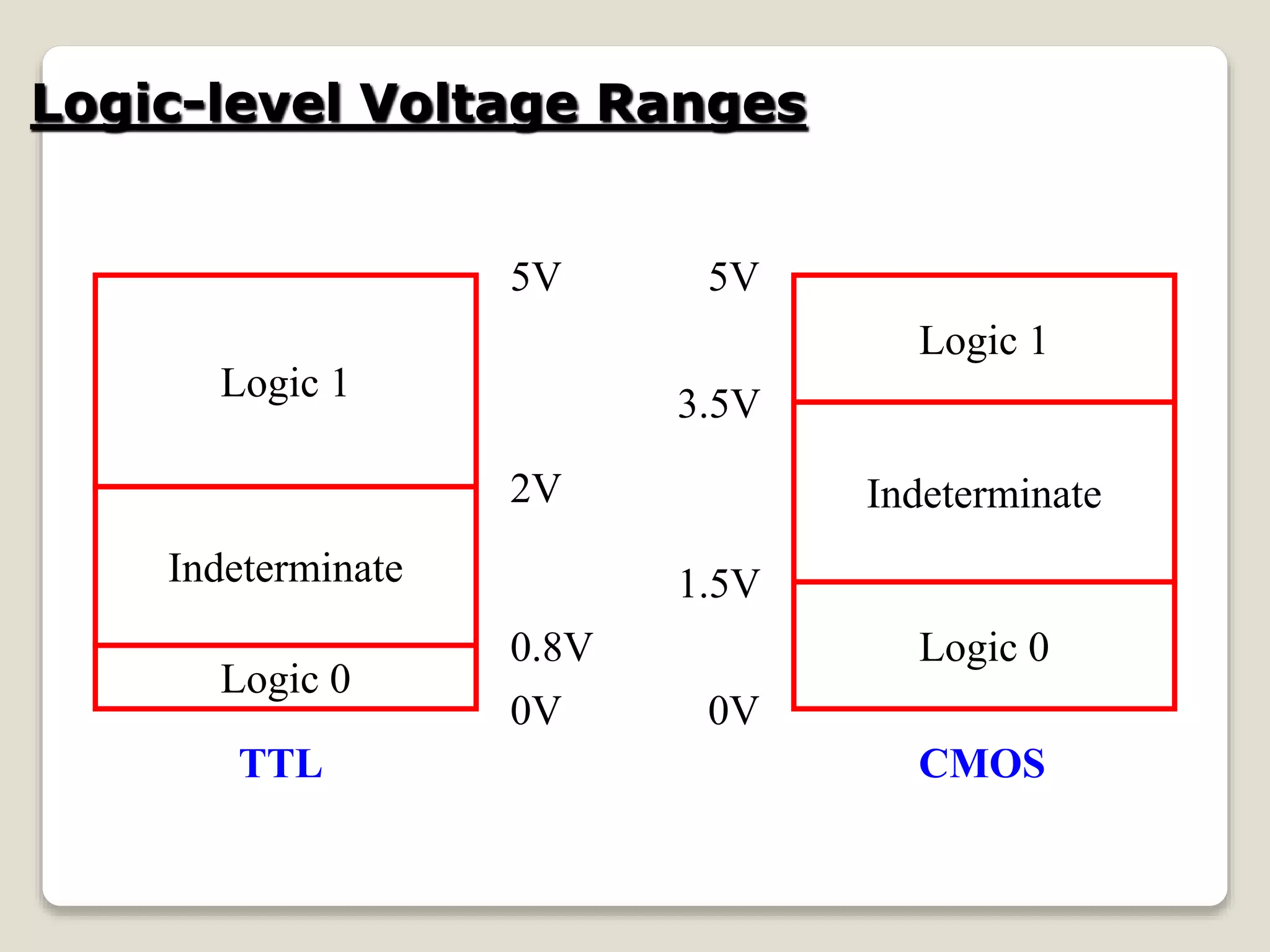
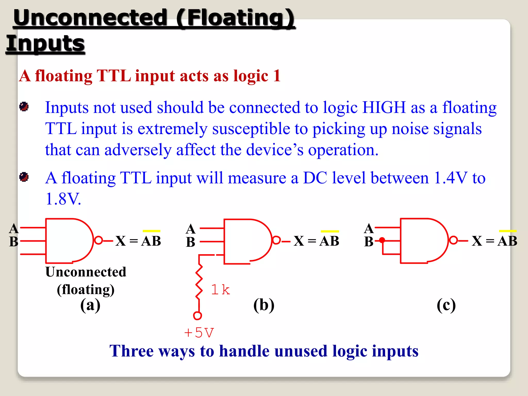
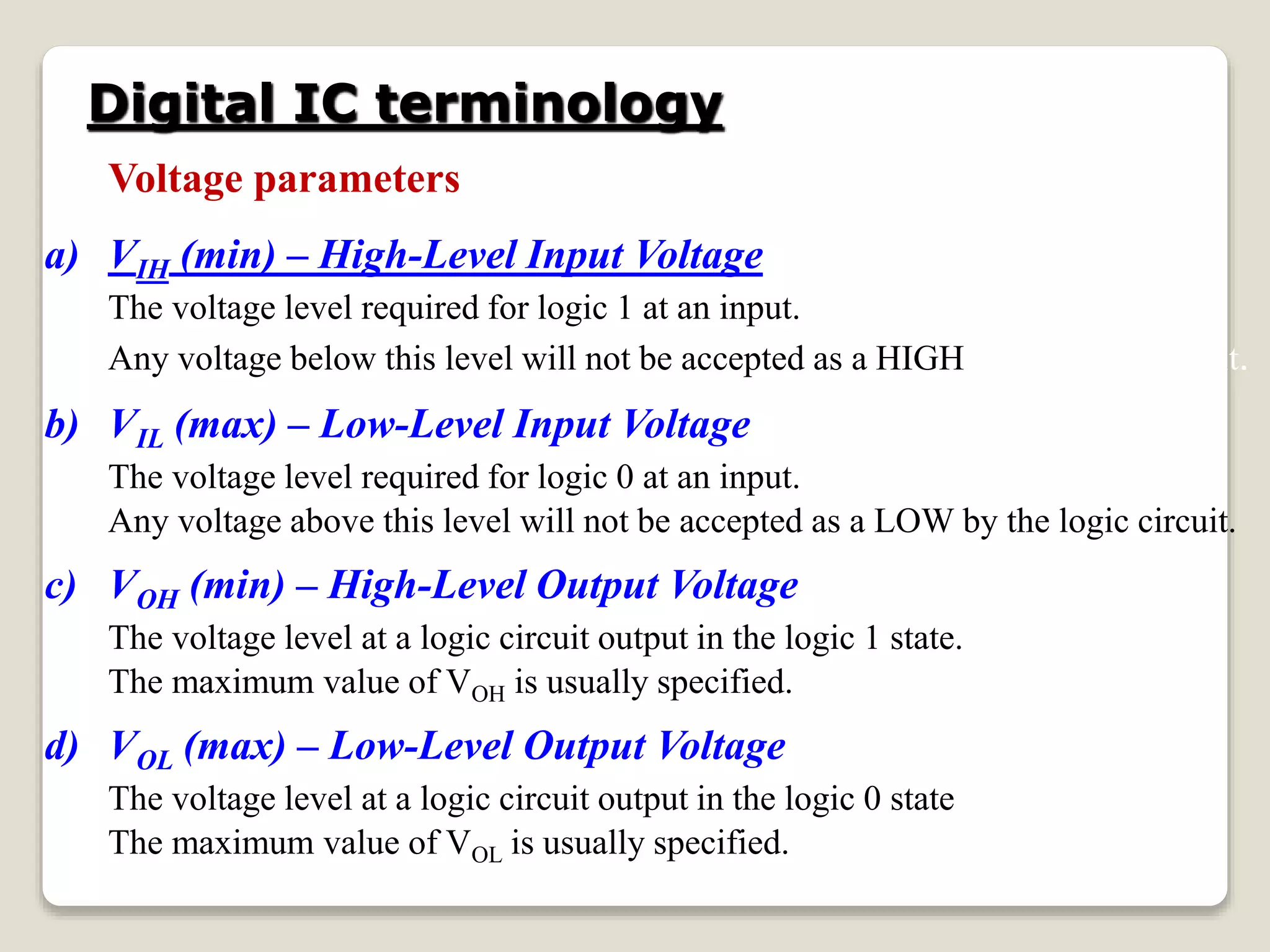
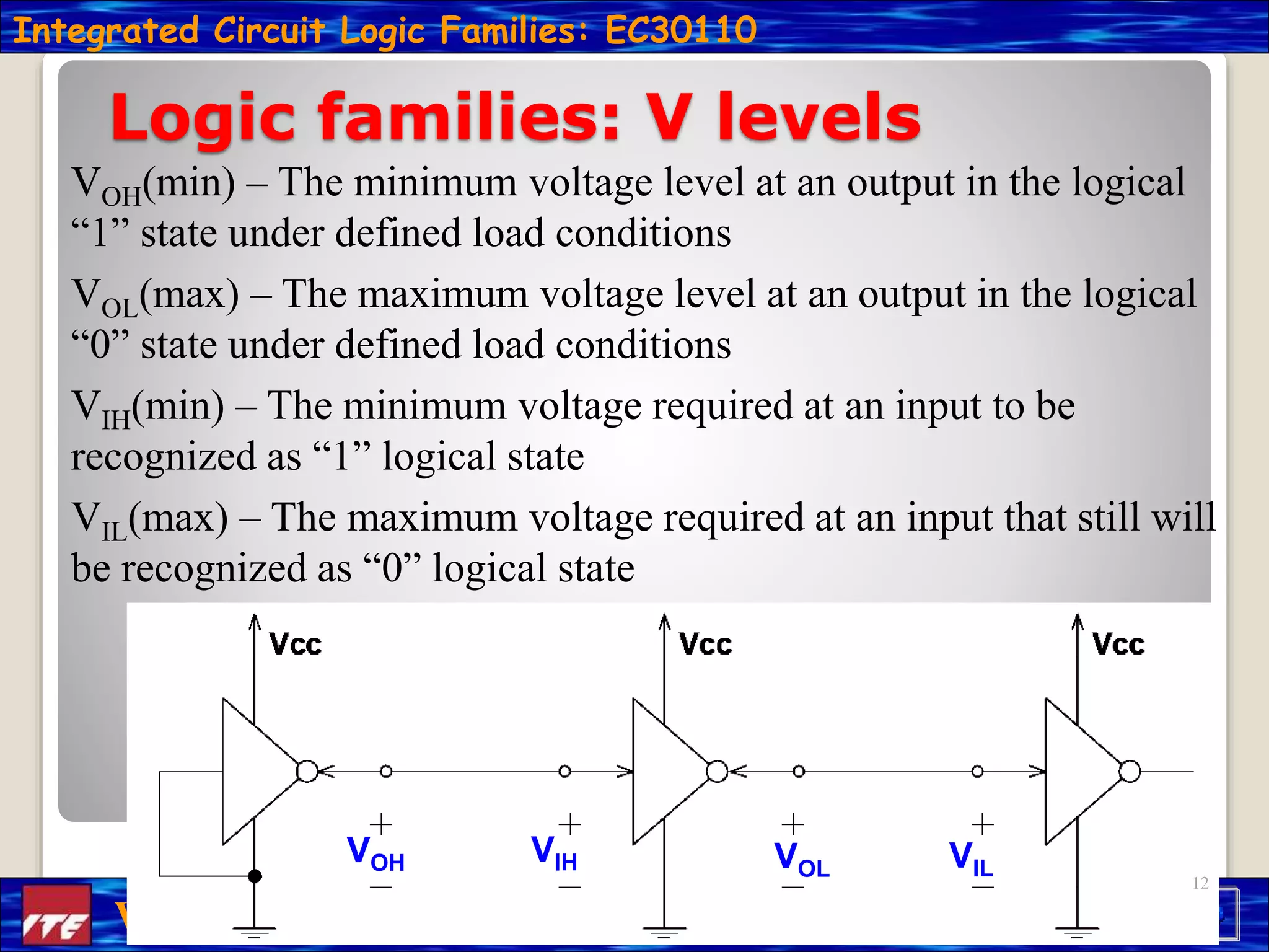
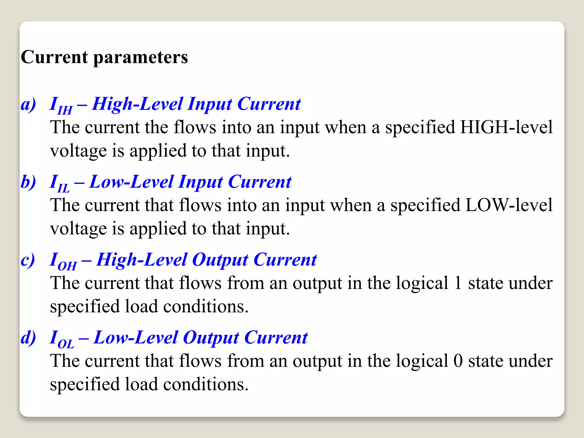
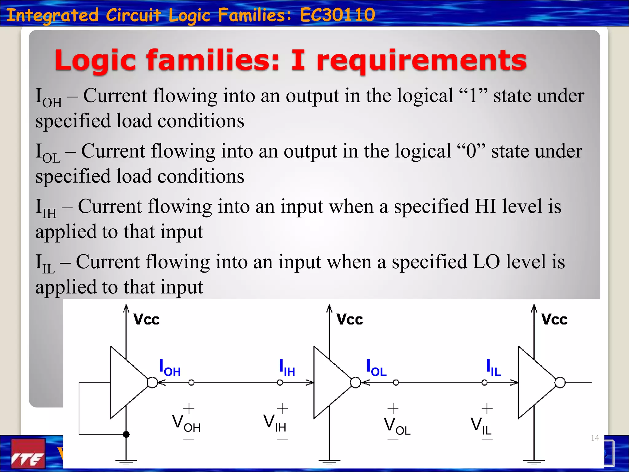
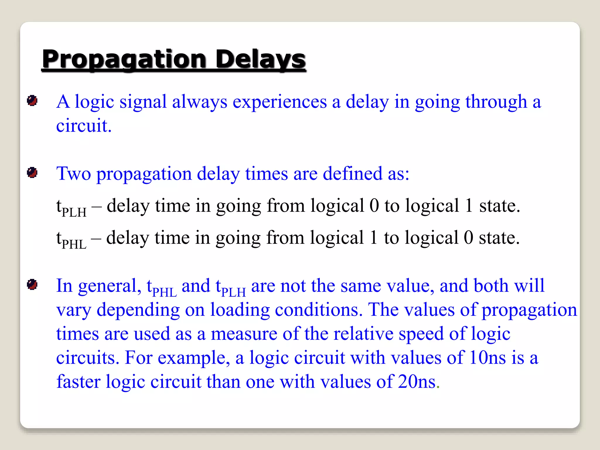
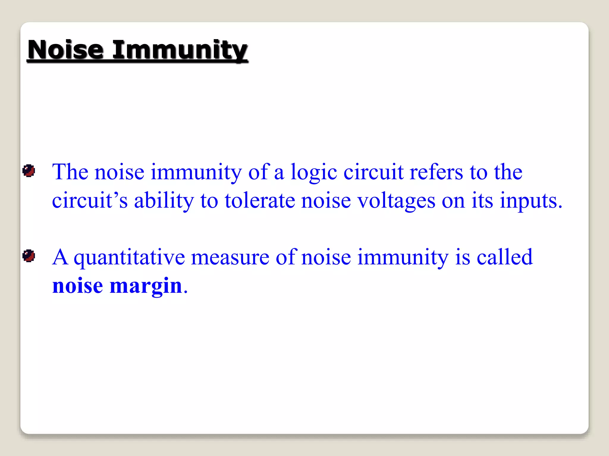
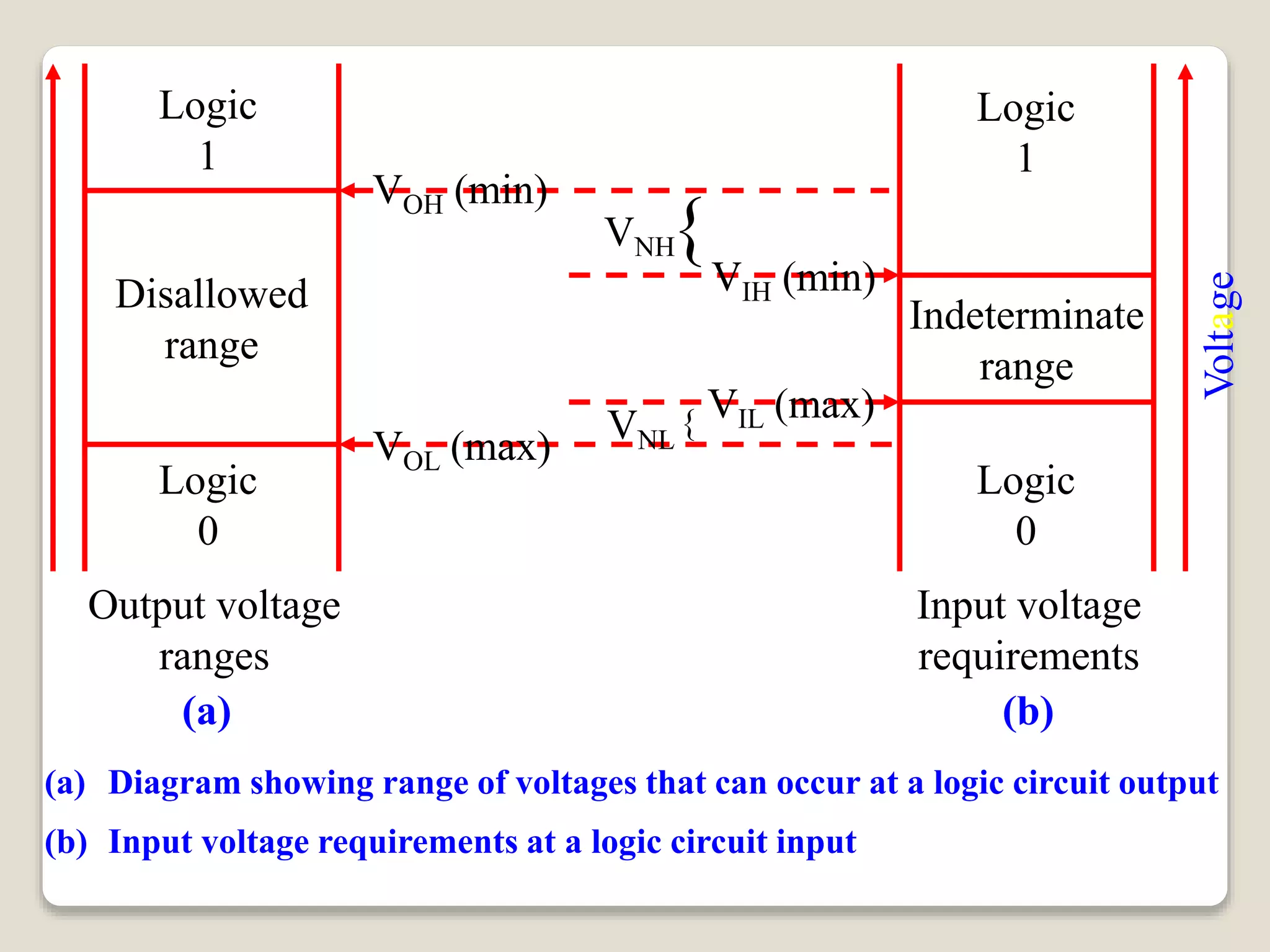
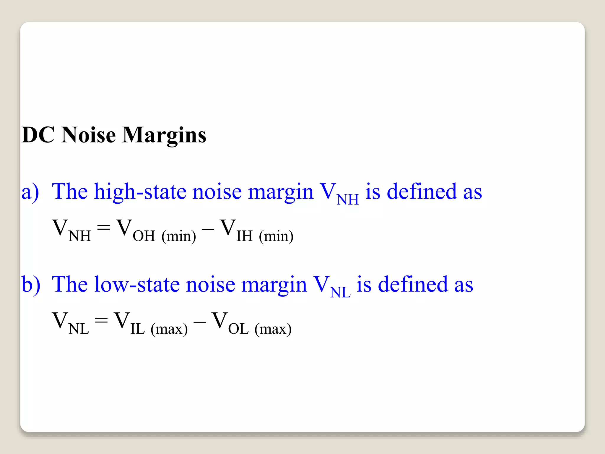
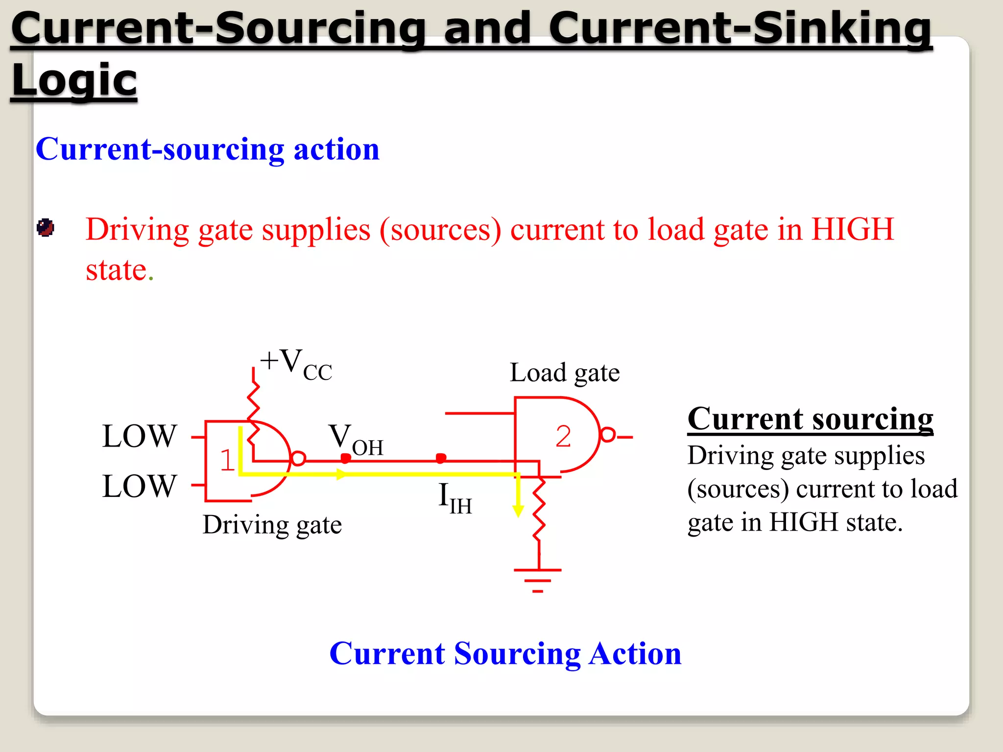
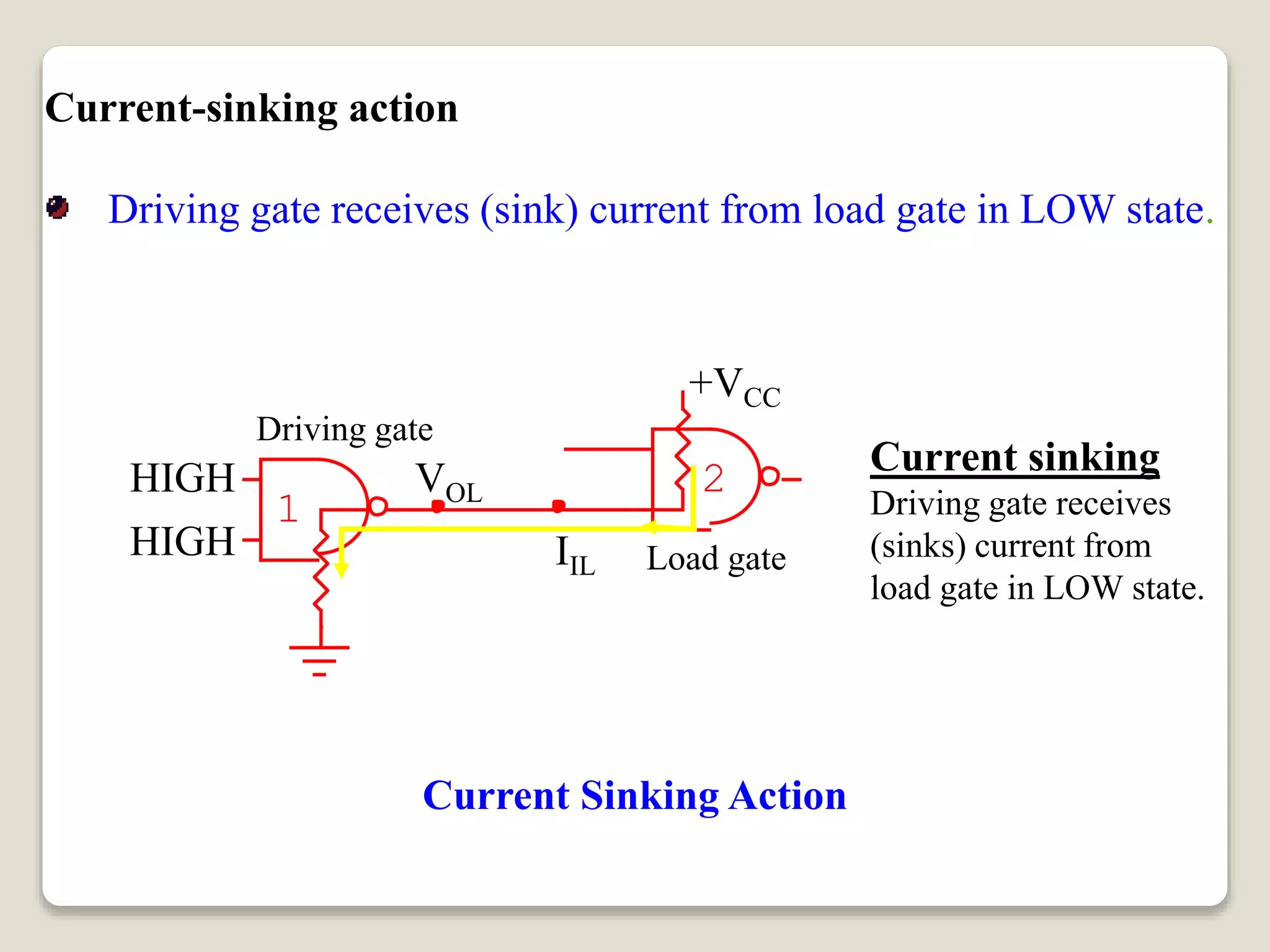
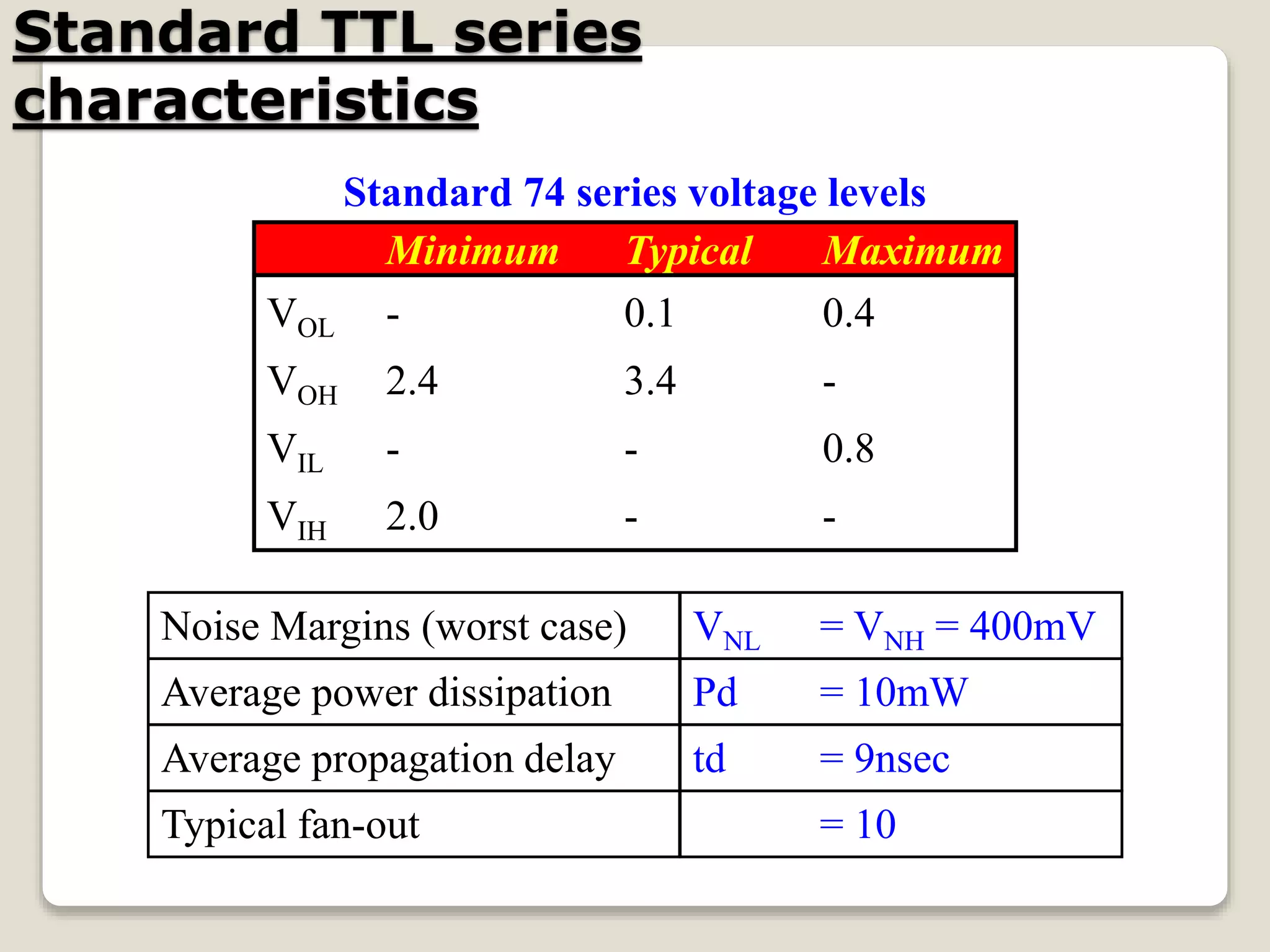
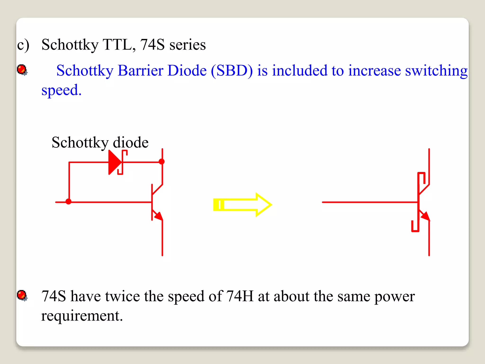
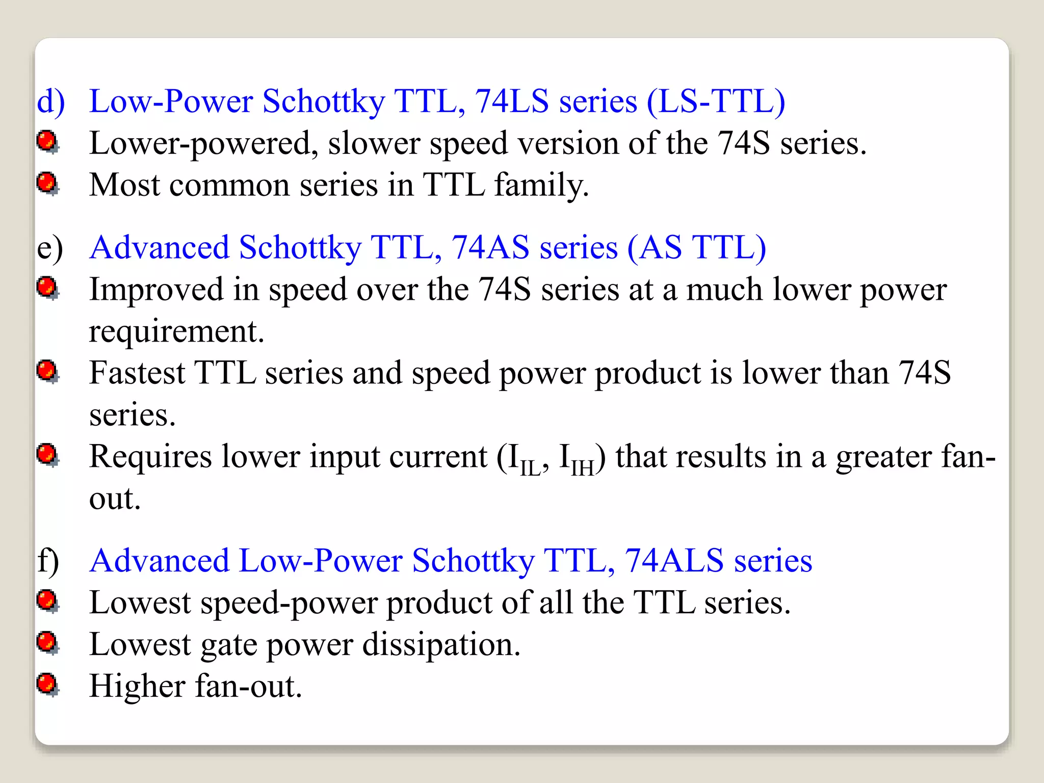
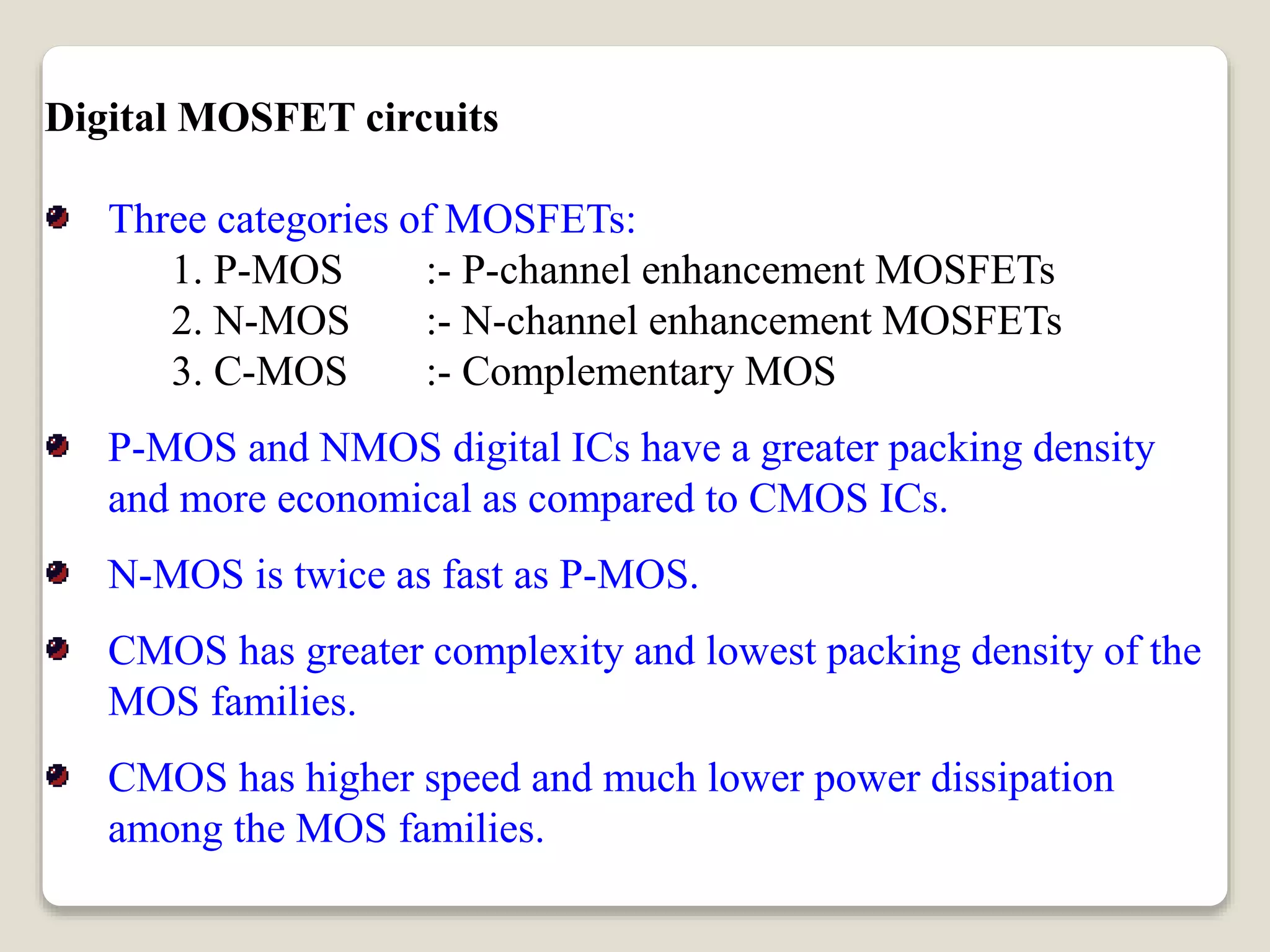
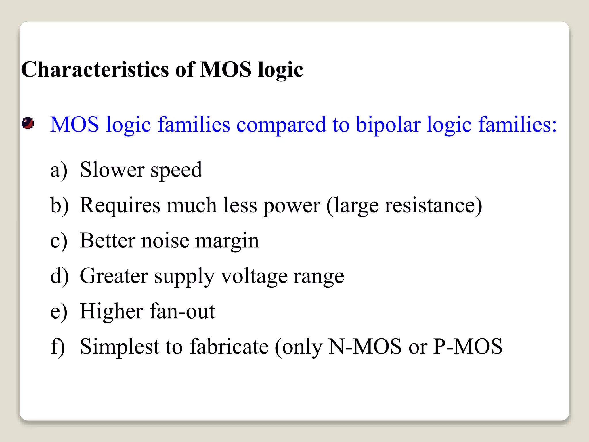
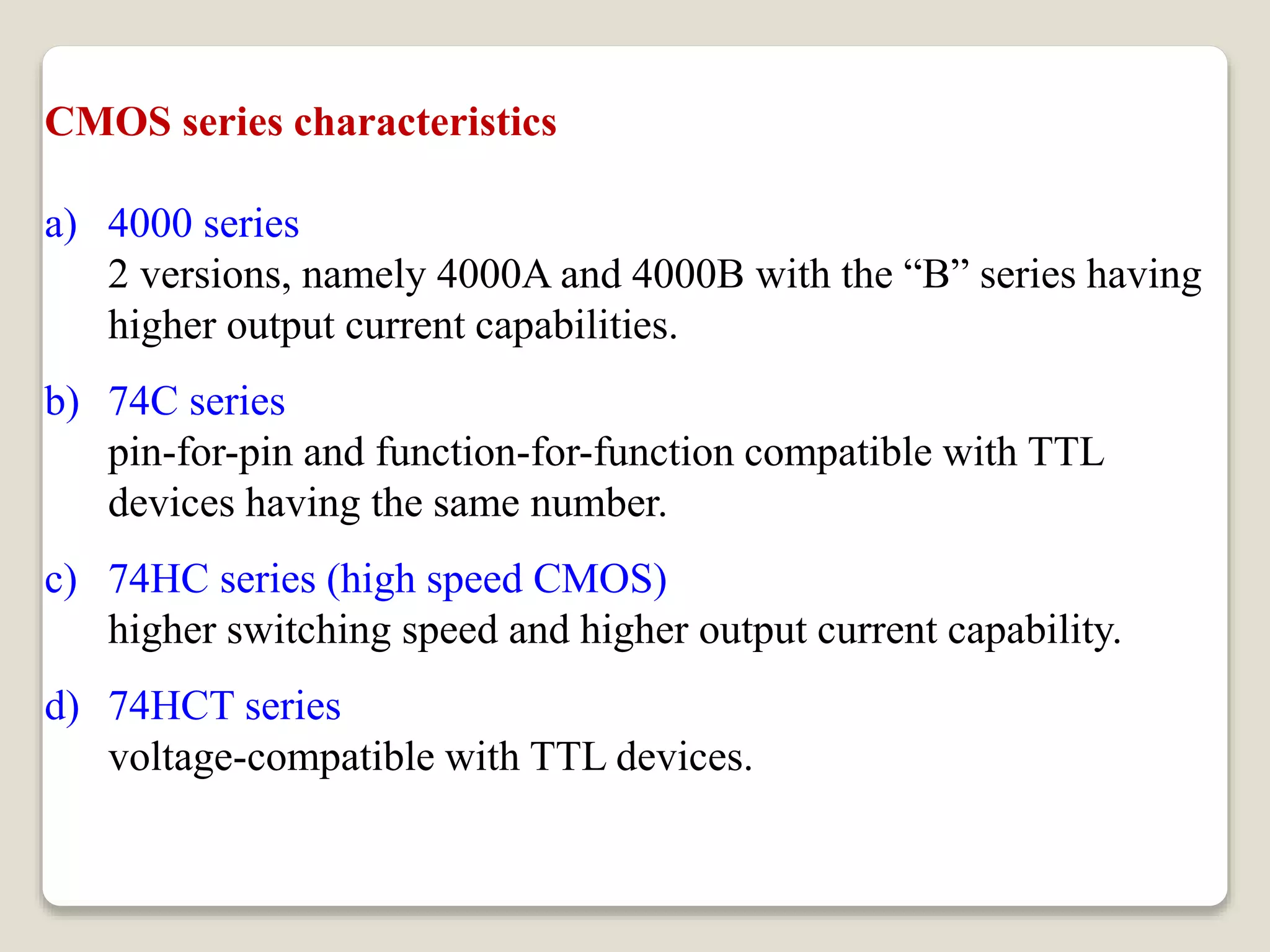
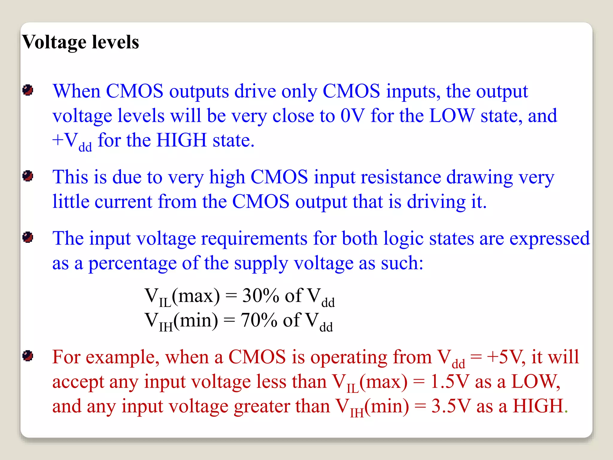
The document describes the specifications of various logic integrated circuits (ICs), including their fan-in, fan-out, input, and output characteristics. It defines common digital IC terminology related to voltage levels, current parameters, propagation delays, and noise immunity. It then examines the characteristics of different logic families, specifically TTL and CMOS. TTL families include standard TTL, low power TTL, high speed TTL, and others. CMOS families include 4000 series and 74C/HC/HCT series. Key specifications like voltage levels, noise margins, and power dissipation are compared between TTL and CMOS logic families.
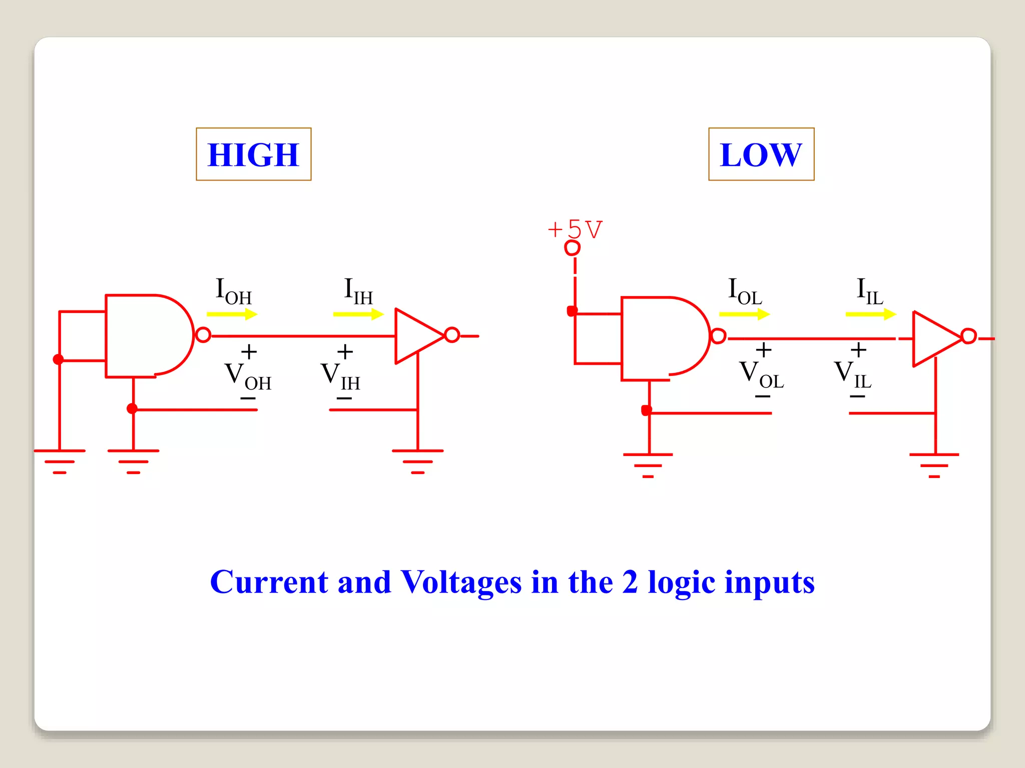
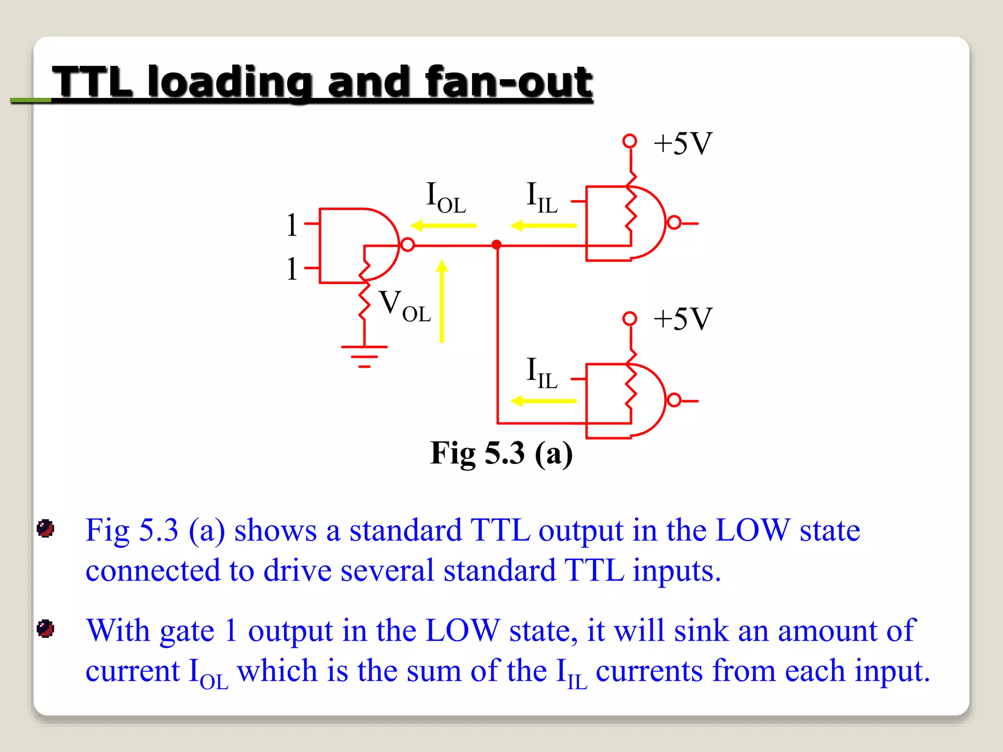
![Determining the Fan-out
To determine how many different inputs an IC output
can drive, one needs to know the current drive
capability of the output [i.e. IOL(max) and IOH(max)] and
the current requirements of each input (i.e. IIL and IIH).](https://image.slidesharecdn.com/icfmaillies-220410053136/75/IC-fmaillies-ppt-28-2048.jpg)


![RF Circuit Design - [Ch2-1] Resonator and Impedance Matching](https://cdn.slidesharecdn.com/ss_thumbnails/ch2-1-150613064353-lva1-app6892-thumbnail.jpg?width=640&height=640&fit=bounds)


