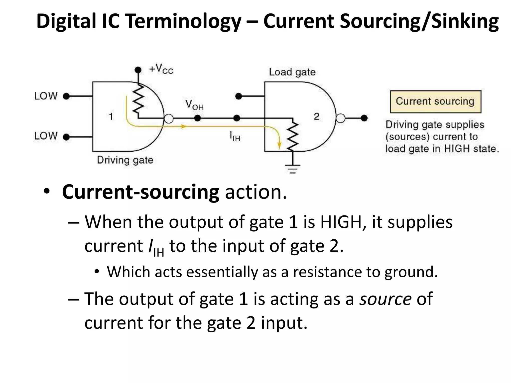
Logic Families
Topics to be Addressed
 Characteristics/ Specification Terminology of ICs
Introduction to different logic families:
 RTL,
TTL,
Metal Oxide Semiconductor.
INTRODUCTION
• Digital IC technology has advanced rapidly from integrations
which can have 1 million or more gates.
• ICs pack more circuitry in a small package, so overall size of
almost any system is reduced.
– Cost is reduced because of the economies of
mass-producing large volumes of similar devices.
• ICs have made digital systems more reliable by reducing the
number of external interconnections from one device to
another.
– Protected from poor soldering, breaks or shorts
in connecting paths on a circuit board, and other
physical problems.
INTRODUCTION
• ICs cannot handle very large currents or voltage.
– Heat generated in such small spaces would cause
temperatures to rise beyond acceptable limits.
• For higher power levels, an interfacing circuit will be needed—
typically of components or special power ICs.
• ICs can’t easily implement certain devices such
as inductors, transformers, and large capacitors.
– Principally used to perform low-power circuit operations—
commonly called information processing.
• Various logic families differ in major components
in their circuitry.
– RTL, TTL and ECL use bipolar transistors as their
major circuit element.
– PMOS, NMOS, and CMOS use unipolar MOSFET
transistors.
IC nomenclature & terminology
is fairly standardized.
IC nomenclature & terminology
is fairly standardized.
Digital IC Terminology – Fan Out
• A logic-circuit output is generally required to
drive several logic inputs.
– Sometimes all ICs are from the same logic family.
• But many systems have a mix of various logic families.
– The fan-out—loading factor—is the maximum
number of logic inputs an output can drive reliably.
Digital IC Terminology – Propagation Delay
• A logic signal always experiences a delay
going through a circuit.
– The two propagation delay times are defined as:
Propagation
delays.
Digital IC Terminology – Power
Requirements
• Every IC requires a certain amount of electrical
power to operate.
– Supplied by one or more power-supply voltages
connected at VCC (TTL) or VDD (MOS devices).
– For many ICs, current drawn from the supply varies
depending on logic states of the circuits on the chip.
Digital IC Terminology – Power
Requirements
• The amount of power an IC requires is
determined by the current, ICC (or IDD) it draws
from the supply.
– Actual power is the product ICC x VCC (IDD x VDD ).
In some logic circuits, average
current is computed based
on the assumption that gate
outputs are LOW half the
time and HIGH half the time.
Digital IC Terminology – Power Requirements
can be rewritten to calculate
average power dissipated:
• The amount of power an IC requires is determined
by the current, ICC (or IDD) it draws from the supply.
– Actual power is the product ICC x VCC (IDD x VDD ).
Digital IC Terminology – Noise
• Stray electric/magnetic fields can induce
voltages on the connecting wires between logic
circuits
– Called noise, these unwanted, spurious signals can
sometimes cause unpredictable operation.
Digital IC Terminology – Noise
• Noise immunity refers to the circuit’s ability to tolerate
noise without changes in output voltage.
– A quantitative measure is called noise margin.
High-state noise
margin:
Low-state noise
margin:
Digital IC Terminology – Invalid Voltage
• For proper operation, logic circuit input voltage
levels must be kept out of the indeterminate
range.
– Lower than VIL(max) or higher than VIH (min).
• Invalid voltage will produce unpredictable output.
• It is important to know valid voltage ranges for
the logic family being used so invalid conditions
can be recognized when testing or
troubleshooting.
• Logic families can be described by how current
flows between the output of one logic circuit
and the input of another.
Digital IC Terminology – Current Sourcing/Sinking
• Current-sourcing action.
– When the output of gate 1 is HIGH, it supplies
current IIH to the input of gate 2.
• Which acts essentially as a resistance to ground.
– The output of gate 1 is acting as a source of
current for the gate 2 input.
Digital IC Terminology – Current Sourcing/Sinking
• Current-sinking action.
– Input circuitry of gate 2 is represented as a resistance tied to +VCC —
the positive terminal of a power supply.
– When gate 1 output goes LOW, current will flow from the input circuit
of gate 2 back through the output resistance of gate 1, to ground.
• Circuit output that drives the input of gate 2 must be able to sink a
current, IIL , coming from that input.
RTL (Register Transistor Logic)
 It is no longer used theses days
 But was the first commercial family to be used
extensively
 The basic digital circuit in any IC family is NAND or NOR
 The basic circuit of RTL digital family is NOR gates
 It uses bipolar junction transistors as npn or pnp
The TTL Logic Family
• Most TTL circuits have a similar structure
– NAND and AND gates use multiple-emitter transistor or
multiple diode junction inputs.
– NOR and OR gates use separate input transistors.
• The input will be the cathode of a P-N junction
– A HIGH input will turn off the junction.
• Only a leakage current is generated.
– A LOW input turns on the junction.
• Relatively large current is generated.
• Most TTL circuits have some type of totem-pole output
configuration.
MOS Technology
• MOS technology derives its name from the basic
structure of a metal electrode, over an oxide
insulator, over a semi-conductor substrate.
– Transistors of MOS technology are field-effect
transistors—called MOSFETs.
The electric field on the metal electrode side of the oxide
insulator has an effect on the resistance of the substrate.
• Most of the MOS digital ICs are constructed
entirely of MOSFETs and no other components.
– MOSFETs are relatively simple and inexpensive
to fabricate, small, and consume very little power.
• The principal disadvantage of MOS devices is
their susceptibility to static-electricity damage.
– Although minimized by proper handling, TTL is
still more durable for laboratory experimentation.
MOS Technology
End of Topic

Logic families

  • 1.
  • 2.
    Topics to beAddressed  Characteristics/ Specification Terminology of ICs Introduction to different logic families:  RTL, TTL, Metal Oxide Semiconductor.
  • 3.
    INTRODUCTION • Digital ICtechnology has advanced rapidly from integrations which can have 1 million or more gates. • ICs pack more circuitry in a small package, so overall size of almost any system is reduced. – Cost is reduced because of the economies of mass-producing large volumes of similar devices. • ICs have made digital systems more reliable by reducing the number of external interconnections from one device to another. – Protected from poor soldering, breaks or shorts in connecting paths on a circuit board, and other physical problems.
  • 4.
    INTRODUCTION • ICs cannothandle very large currents or voltage. – Heat generated in such small spaces would cause temperatures to rise beyond acceptable limits. • For higher power levels, an interfacing circuit will be needed— typically of components or special power ICs. • ICs can’t easily implement certain devices such as inductors, transformers, and large capacitors. – Principally used to perform low-power circuit operations— commonly called information processing.
  • 5.
    • Various logicfamilies differ in major components in their circuitry. – RTL, TTL and ECL use bipolar transistors as their major circuit element. – PMOS, NMOS, and CMOS use unipolar MOSFET transistors.
  • 6.
    IC nomenclature &terminology is fairly standardized.
  • 7.
    IC nomenclature &terminology is fairly standardized.
  • 8.
    Digital IC Terminology– Fan Out • A logic-circuit output is generally required to drive several logic inputs. – Sometimes all ICs are from the same logic family. • But many systems have a mix of various logic families. – The fan-out—loading factor—is the maximum number of logic inputs an output can drive reliably.
  • 9.
    Digital IC Terminology– Propagation Delay • A logic signal always experiences a delay going through a circuit. – The two propagation delay times are defined as: Propagation delays.
  • 10.
    Digital IC Terminology– Power Requirements • Every IC requires a certain amount of electrical power to operate. – Supplied by one or more power-supply voltages connected at VCC (TTL) or VDD (MOS devices). – For many ICs, current drawn from the supply varies depending on logic states of the circuits on the chip.
  • 11.
    Digital IC Terminology– Power Requirements • The amount of power an IC requires is determined by the current, ICC (or IDD) it draws from the supply. – Actual power is the product ICC x VCC (IDD x VDD ). In some logic circuits, average current is computed based on the assumption that gate outputs are LOW half the time and HIGH half the time.
  • 12.
    Digital IC Terminology– Power Requirements can be rewritten to calculate average power dissipated: • The amount of power an IC requires is determined by the current, ICC (or IDD) it draws from the supply. – Actual power is the product ICC x VCC (IDD x VDD ).
  • 13.
    Digital IC Terminology– Noise • Stray electric/magnetic fields can induce voltages on the connecting wires between logic circuits – Called noise, these unwanted, spurious signals can sometimes cause unpredictable operation.
  • 14.
    Digital IC Terminology– Noise • Noise immunity refers to the circuit’s ability to tolerate noise without changes in output voltage. – A quantitative measure is called noise margin. High-state noise margin: Low-state noise margin:
  • 15.
    Digital IC Terminology– Invalid Voltage • For proper operation, logic circuit input voltage levels must be kept out of the indeterminate range. – Lower than VIL(max) or higher than VIH (min). • Invalid voltage will produce unpredictable output. • It is important to know valid voltage ranges for the logic family being used so invalid conditions can be recognized when testing or troubleshooting. • Logic families can be described by how current flows between the output of one logic circuit and the input of another.
  • 16.
    Digital IC Terminology– Current Sourcing/Sinking • Current-sourcing action. – When the output of gate 1 is HIGH, it supplies current IIH to the input of gate 2. • Which acts essentially as a resistance to ground. – The output of gate 1 is acting as a source of current for the gate 2 input.
  • 17.
    Digital IC Terminology– Current Sourcing/Sinking • Current-sinking action. – Input circuitry of gate 2 is represented as a resistance tied to +VCC — the positive terminal of a power supply. – When gate 1 output goes LOW, current will flow from the input circuit of gate 2 back through the output resistance of gate 1, to ground. • Circuit output that drives the input of gate 2 must be able to sink a current, IIL , coming from that input.
  • 18.
    RTL (Register TransistorLogic)  It is no longer used theses days  But was the first commercial family to be used extensively  The basic digital circuit in any IC family is NAND or NOR  The basic circuit of RTL digital family is NOR gates  It uses bipolar junction transistors as npn or pnp
  • 19.
    The TTL LogicFamily • Most TTL circuits have a similar structure – NAND and AND gates use multiple-emitter transistor or multiple diode junction inputs. – NOR and OR gates use separate input transistors. • The input will be the cathode of a P-N junction – A HIGH input will turn off the junction. • Only a leakage current is generated. – A LOW input turns on the junction. • Relatively large current is generated. • Most TTL circuits have some type of totem-pole output configuration.
  • 20.
    MOS Technology • MOStechnology derives its name from the basic structure of a metal electrode, over an oxide insulator, over a semi-conductor substrate. – Transistors of MOS technology are field-effect transistors—called MOSFETs. The electric field on the metal electrode side of the oxide insulator has an effect on the resistance of the substrate. • Most of the MOS digital ICs are constructed entirely of MOSFETs and no other components. – MOSFETs are relatively simple and inexpensive to fabricate, small, and consume very little power.
  • 21.
    • The principaldisadvantage of MOS devices is their susceptibility to static-electricity damage. – Although minimized by proper handling, TTL is still more durable for laboratory experimentation. MOS Technology
  • 22.