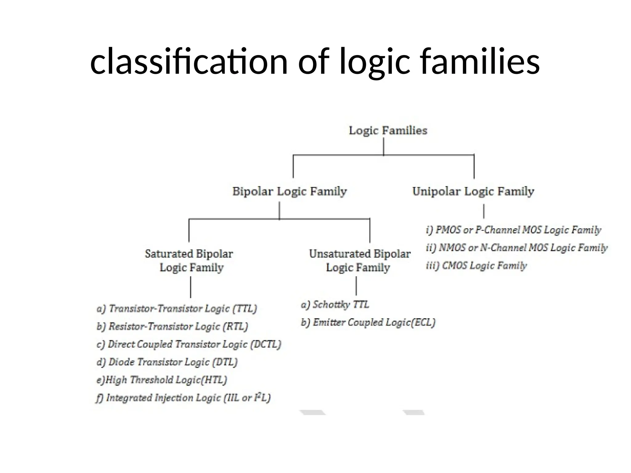
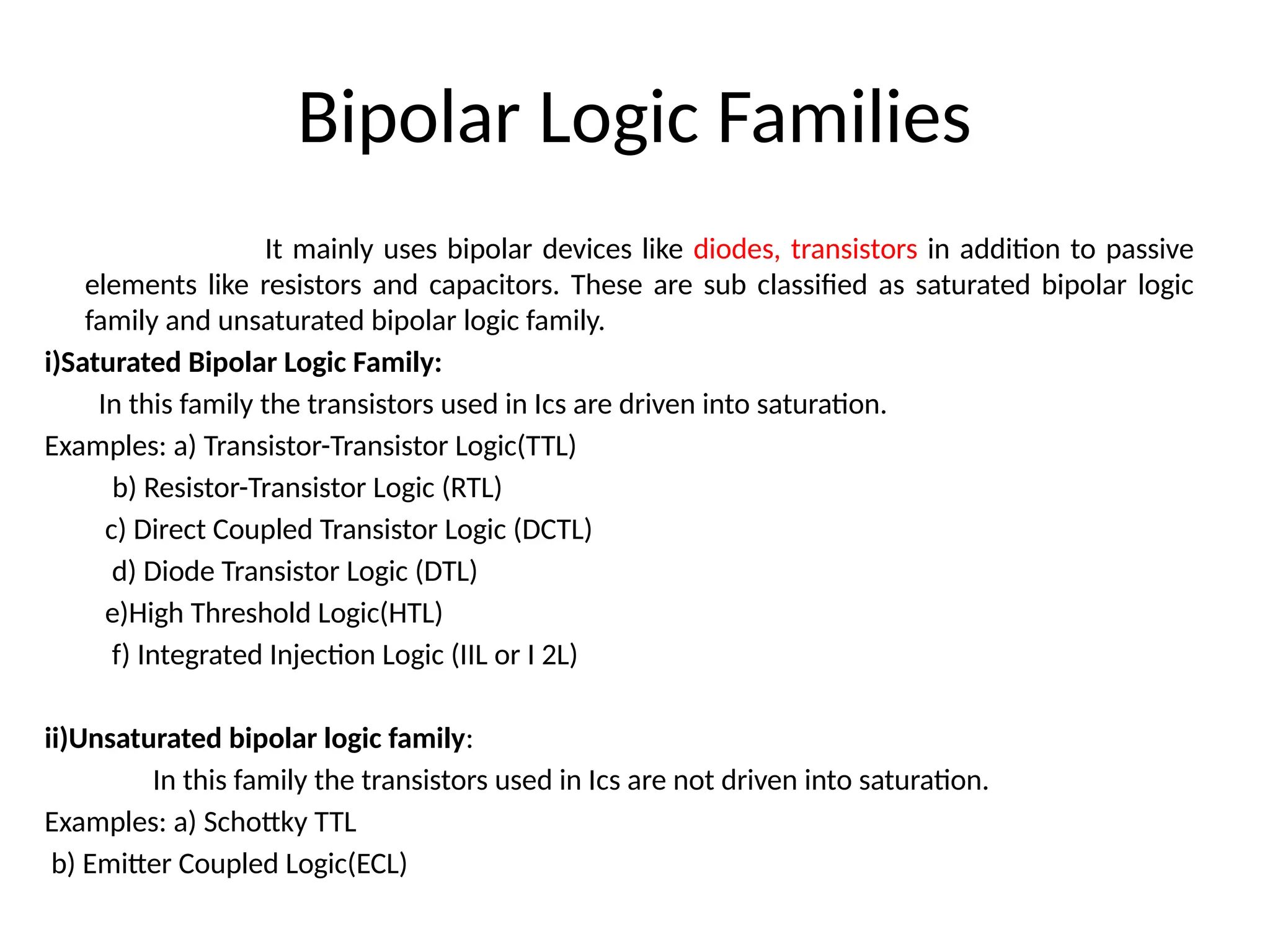
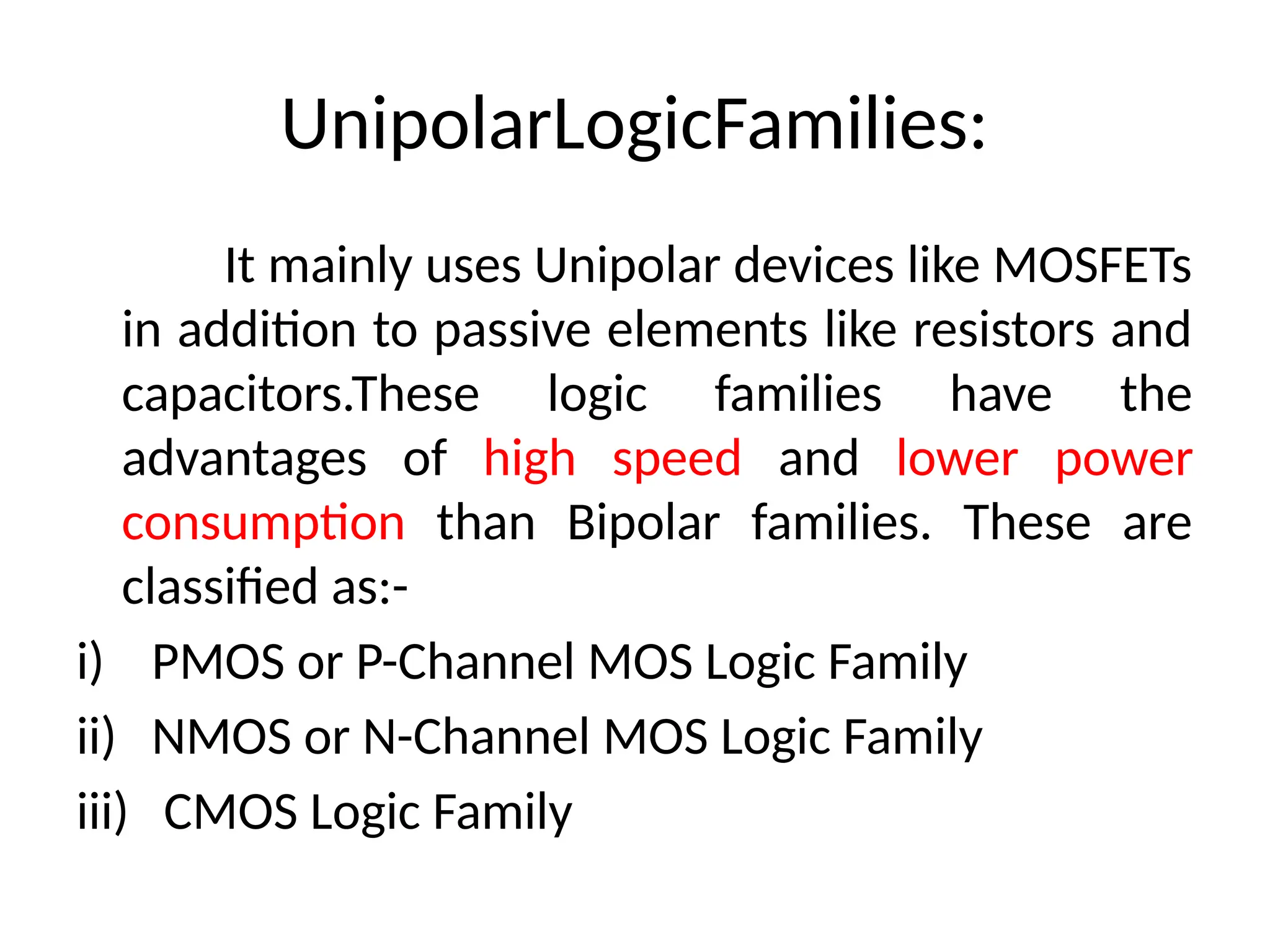
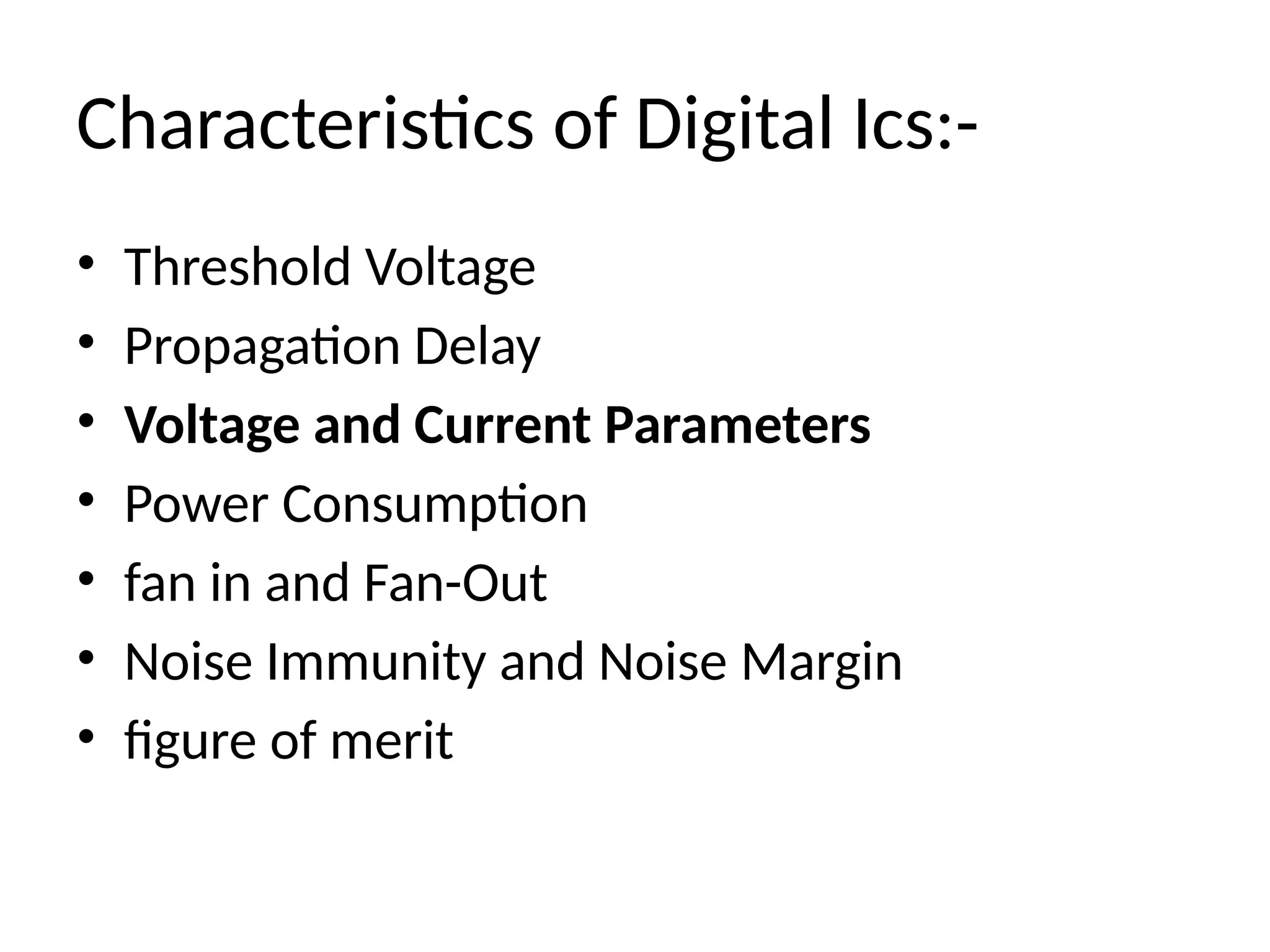
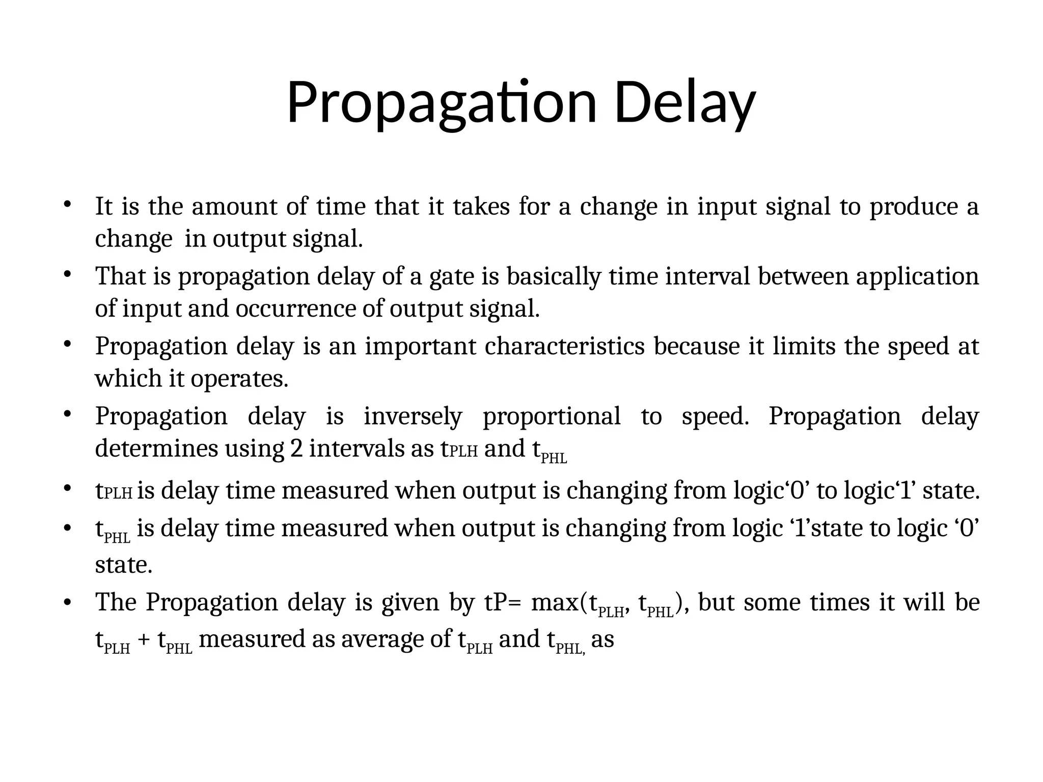
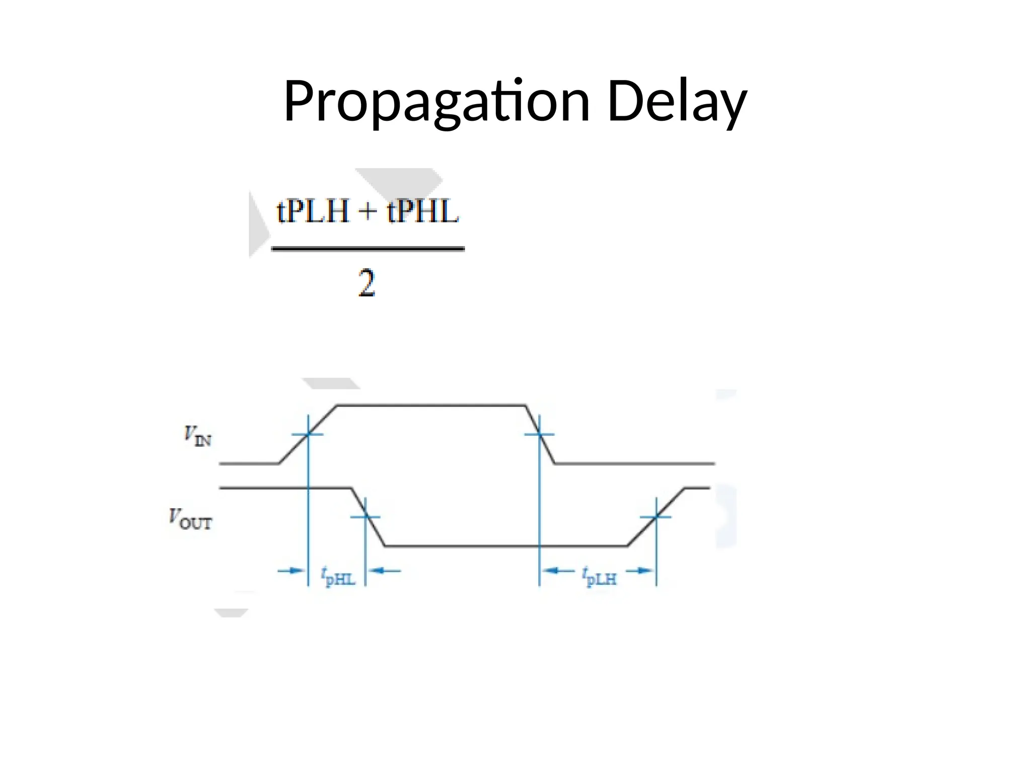
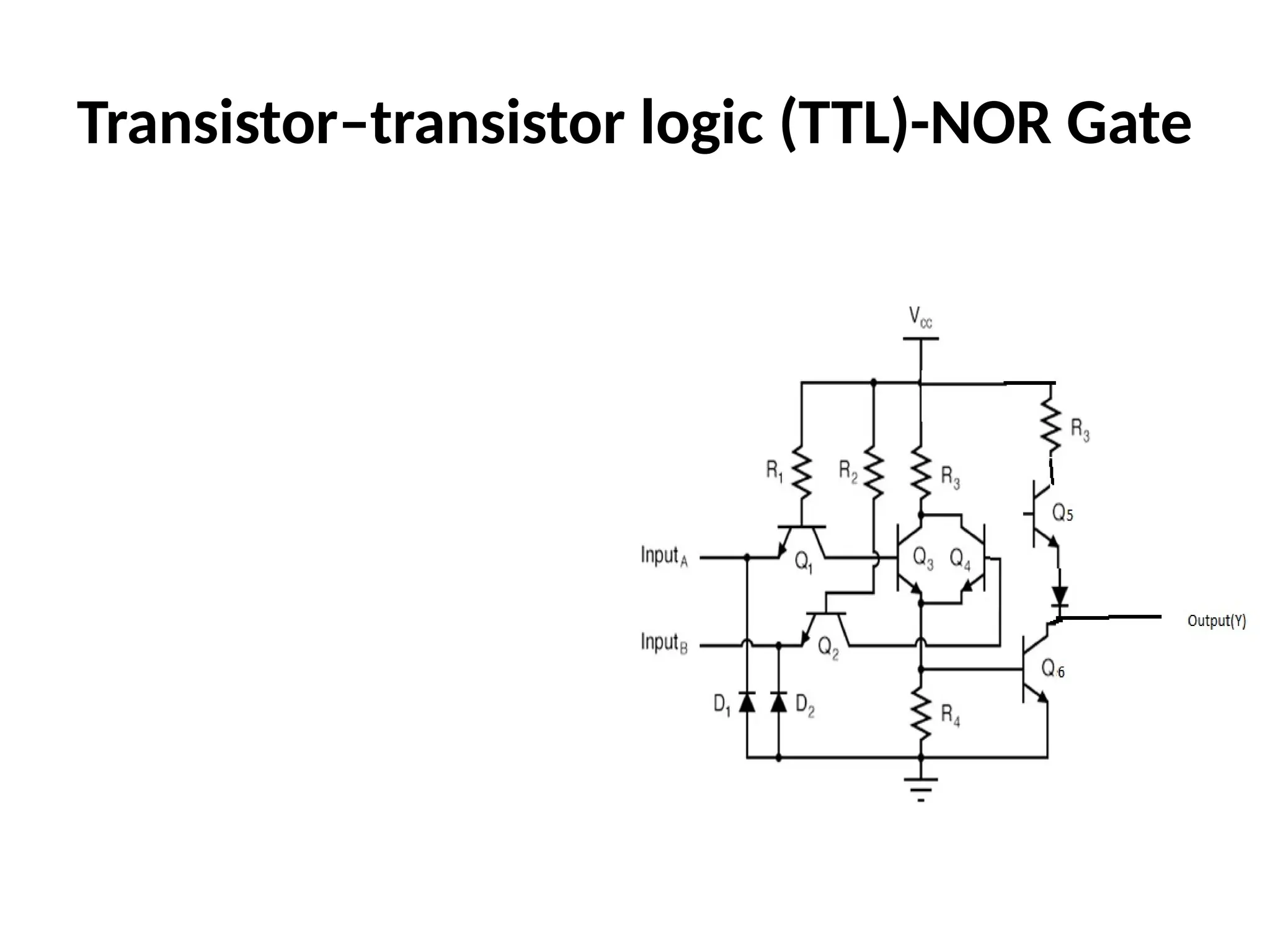
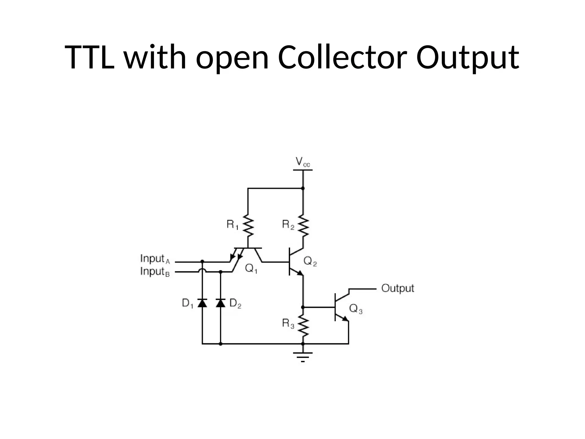
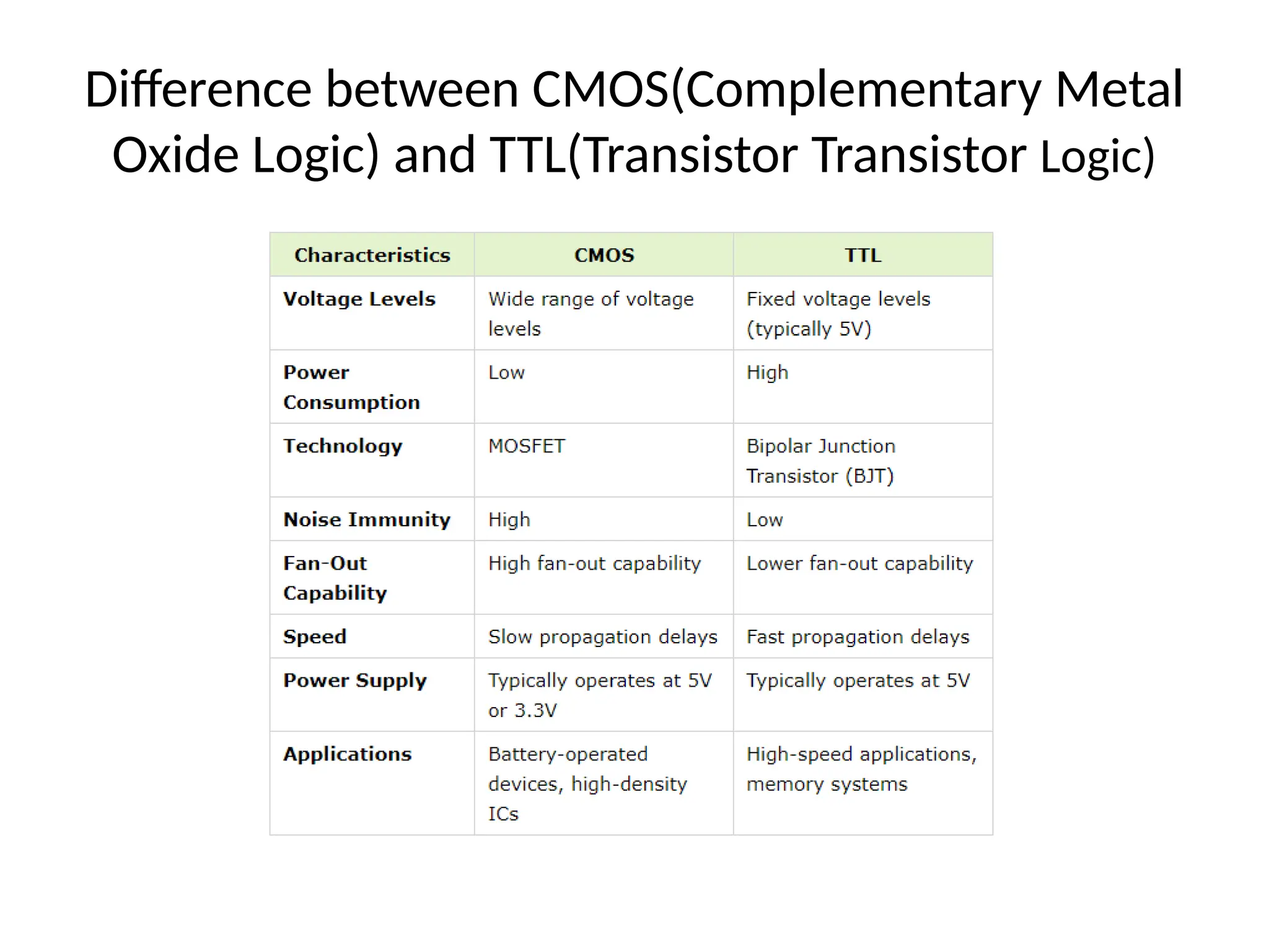
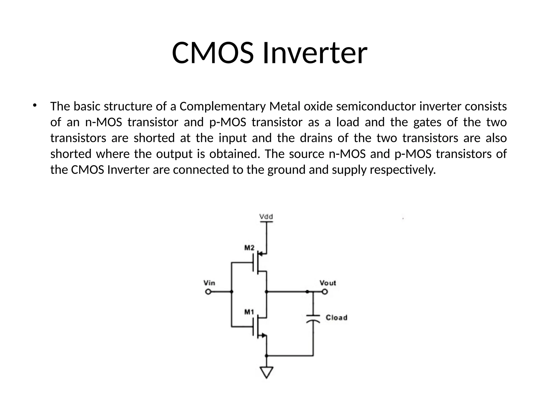
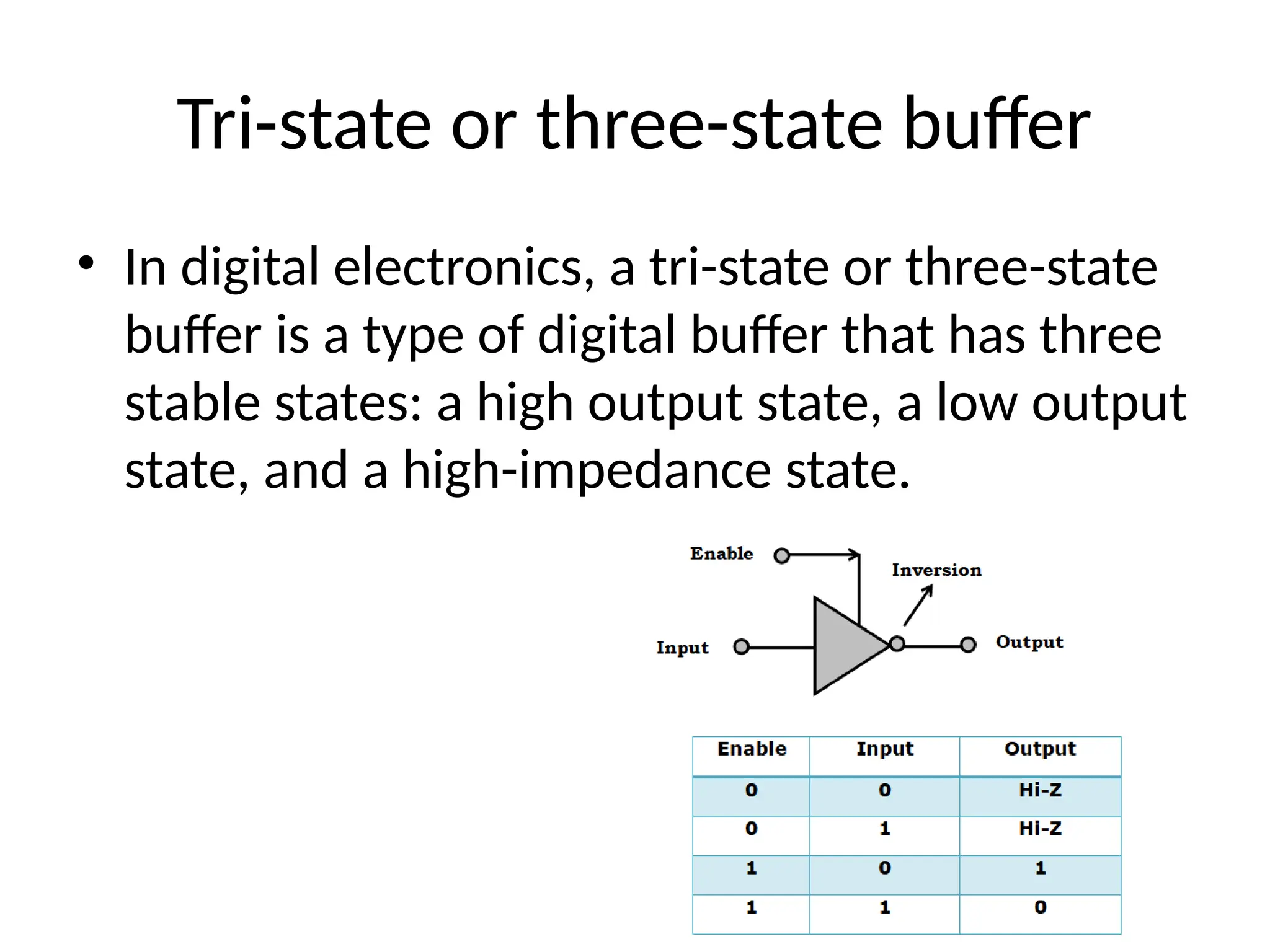
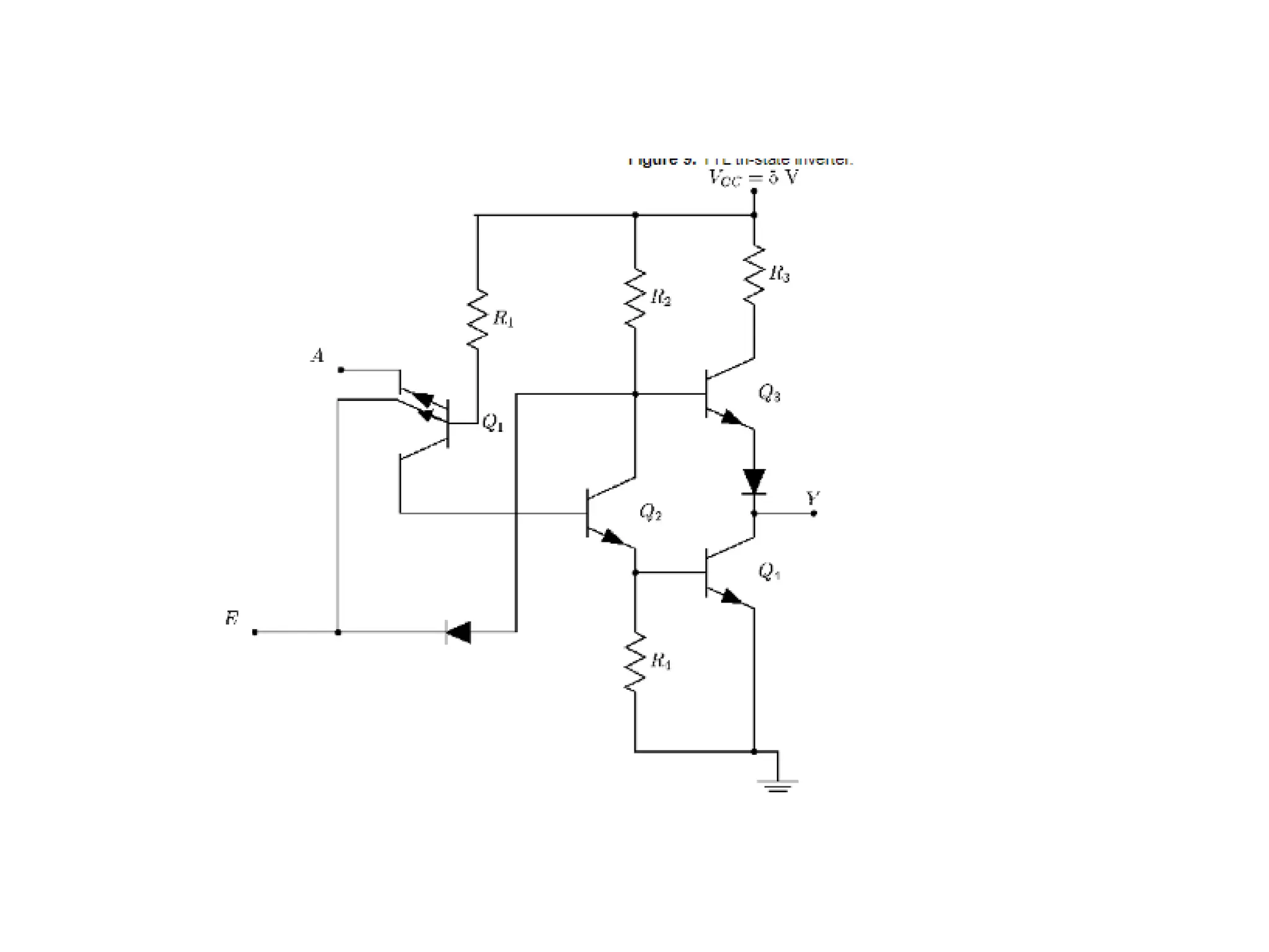
Chapter No 4
logic families
logic family
• A logic family of monolithic(Single) digital
integrated circuit devices is a group of
electronic logic gates constructed using one of
several different designs and different
production technologies, usually with
compatible logic levels and power supply
characteristics within a family.
classification of logic families
Bipolar Logic Families
It mainly uses bipolar devices like diodes, transistors in addition to passive
elements like resistors and capacitors. These are sub classified as saturated bipolar logic
family and unsaturated bipolar logic family.
i)Saturated Bipolar Logic Family:
In this family the transistors used in Ics are driven into saturation.
Examples: a) Transistor-Transistor Logic(TTL)
b) Resistor-Transistor Logic (RTL)
c) Direct Coupled Transistor Logic (DCTL)
d) Diode Transistor Logic (DTL)
e)High Threshold Logic(HTL)
f) Integrated Injection Logic (IIL or I 2L)
ii)Unsaturated bipolar logic family:
In this family the transistors used in Ics are not driven into saturation.
Examples: a) Schottky TTL
b) Emitter Coupled Logic(ECL)
UnipolarLogicFamilies:
It mainly uses Unipolar devices like MOSFETs
in addition to passive elements like resistors and
capacitors.These logic families have the
advantages of high speed and lower power
consumption than Bipolar families. These are
classified as:-
i) PMOS or P-Channel MOS Logic Family
ii) NMOS or N-Channel MOS Logic Family
iii) CMOS Logic Family
Characteristics of Digital Ics:-
• Threshold Voltage
• Propagation Delay
• Voltage and Current Parameters
• Power Consumption
• fan in and Fan-Out
• Noise Immunity and Noise Margin
• figure of merit
Threshold Voltage
• It is the value if input voltage at which the
output of logic gate makes transition from one
state to another. It is denoted by VTH.
Propagation Delay
• It is the amount of time that it takes for a change in input signal to produce a
change in output signal.
• That is propagation delay of a gate is basically time interval between application
of input and occurrence of output signal.
• Propagation delay is an important characteristics because it limits the speed at
which it operates.
• Propagation delay is inversely proportional to speed. Propagation delay
determines using 2 intervals as tPLH and tPHL
• tPLH is delay time measured when output is changing from logic‘0’ to logic‘1’ state.
• tPHL is delay time measured when output is changing from logic ‘1’state to logic ‘0’
state.
• The Propagation delay is given by tP= max(tPLH, tPHL), but some times it will be
tPLH + tPHL measured as average of tPLH and tPHL, as
Propagation Delay
Voltage and Current Parameters
• Voltage Parameters (Threshold Levels):
• Ideally, the input voltage levels of 0V and +5V (for TTL) are called logic 0 and 1 levels respectively.
• However, practically we will not always obtain voltage levels matching exactly to these values.
Therefore it is necessary to define the worst-case input voltages.
• VIL(max) – worst-case low-level input voltage:
• This is the maximum value of input voltage which will be considered as a logic 0 level. If the input
voltage is higher than VIL(max), then it will not be treated as a low (0) input level.
• VIH(min) – worst-case high-level input voltage:
• This is the minimum value of input voltage which will be considered as a logic 1 level. If the input
voltage is lower than VIH(min), then it will not be treated as a high (1) input level.
• VOH(min) – worst-case high-level output voltage:
• This is the minimum value of output voltage which will be considered as a logic 1 level. If the
output voltage is lower than VOH(min), then it will not be treated as a high (1) output level.
• VOL(max) – worst-case low-level output voltage:
• This is the maximum value of output voltage which will be considered as a logic 0 level. If the
input voltage is higher than VOL(max), then it will not be treated as a low (0) output level.
• The voltage parameter can be shown on the digital circuit consisting of gates as shown in the
below figure. Note that the NAND and NOT gates shown can be of TTL, ECL, CMOS, or any other
type.
• Current Parameters :
• IIL – Low-level input Current:
• It is the current that flows into the input when a low-level input voltage in
the specified range is applied.
• IIH – High-level input Current:
• It is the current that flows into the input when a high-level input voltage in
the specified range is applied.
• IOL – Low-level output Current:
• It is the current that flows from the output when the output voltage is in the
specified low voltage range and the specified load is applied.
• IOH – High-level Output Current:
• It is the current that flows from the output when the output voltage is in the
specified high voltage range and the specified load is applied.
Power Consumption:
• Power dissipation is the supplied power
required to operate the desired logic
function.
• Power dissipation is the supplied power
required to operate the desired logic
function.
fan in and Fan-Out
• The fan in is defined as the number of inputs a gate has.
For example, a two-input gate will have a fan-in equal to 2.
• The fan-out in logic gate is number of inputs that the gate
can drive without exceeding its worst case loading
specifications.
• Fan-Out depends not only on the output characteristics
but also on inputs that itis driving
• The LOW state and HIGH state fan-outs of a gate may not
be equal.
Noise Immunity and Noise Margin
• What is Noise?
It is Unwanted signal that mixes with normal signal
.
Sources of noise include the operation environment,
power supply, electric and magnetic fields, and
radiation waves.
• Noise immunity refers to the circuit's ability to
tolerate noise without changes in output voltage.
• Noise margin is a measure of design margins to
ensure circuits functioning properly within specified
conditions.
figure of merit
• The figure of merit of a logic family is the
product of power dissipation and propogation
delay . It is called as speed power product .
• The figure of merit should be as low as
possible .
Transistor–transistor logic (TTL)-NAND Gate
• Transistor–transistor logic (TTL) is a logic family built from
bipolar junction transistors
TTL NAND GATE
It Mainly consist of Three Stages:-
1.Multi-Emitter Transistor
2.Phase Splitter
3.Totem Pole Output
Opeiraton:-
Case 1:
AB=00,01,10
BE Junction is Forward Bias and
BC Junction is Reverse Bias .
Q1 is ON,Q2 is OFF,Q3 is ON,Q4 is
OFF
Case 2:
AB=11
BE Junction is Reverse Bias and
BC Junction is Forward Bias.
Q1is OFF,Q2 is ON,Q3 is OFF,Q4 is
ON.
Q1
Q2
Q3
Q4
Totem pole
• A totem pole is a standard CMOS output
structure where a P-channel MOSFET is
connected in series with an N-Channel
MOSFET and the connection point between
the two is the output.
Transistor–transistor logic (TTL)-NOR Gate
TTL with open Collector Output
Difference between CMOS(Complementary Metal
Oxide Logic) and TTL(Transistor Transistor Logic)
CMOS Inverter
• The basic structure of a Complementary Metal oxide semiconductor inverter consists
of an n-MOS transistor and p-MOS transistor as a load and the gates of the two
transistors are shorted at the input and the drains of the two transistors are also
shorted where the output is obtained. The source n-MOS and p-MOS transistors of
the CMOS Inverter are connected to the ground and supply respectively.
Tri-state or three-state buffer
• In digital electronics, a tri-state or three-state
buffer is a type of digital buffer that has three
stable states: a high output state, a low output
state, and a high-impedance state.
Pt on logic family for digital electronics in se computer of first semester on topic number five. There is construction working types of logic family according to syllabus .

Pt on logic family for digital electronics in se computer of first semester on topic number five. There is construction working types of logic family according to syllabus .

  • 1.
  • 2.
    logic family • Alogic family of monolithic(Single) digital integrated circuit devices is a group of electronic logic gates constructed using one of several different designs and different production technologies, usually with compatible logic levels and power supply characteristics within a family.
  • 3.
  • 4.
    Bipolar Logic Families Itmainly uses bipolar devices like diodes, transistors in addition to passive elements like resistors and capacitors. These are sub classified as saturated bipolar logic family and unsaturated bipolar logic family. i)Saturated Bipolar Logic Family: In this family the transistors used in Ics are driven into saturation. Examples: a) Transistor-Transistor Logic(TTL) b) Resistor-Transistor Logic (RTL) c) Direct Coupled Transistor Logic (DCTL) d) Diode Transistor Logic (DTL) e)High Threshold Logic(HTL) f) Integrated Injection Logic (IIL or I 2L) ii)Unsaturated bipolar logic family: In this family the transistors used in Ics are not driven into saturation. Examples: a) Schottky TTL b) Emitter Coupled Logic(ECL)
  • 5.
    UnipolarLogicFamilies: It mainly usesUnipolar devices like MOSFETs in addition to passive elements like resistors and capacitors.These logic families have the advantages of high speed and lower power consumption than Bipolar families. These are classified as:- i) PMOS or P-Channel MOS Logic Family ii) NMOS or N-Channel MOS Logic Family iii) CMOS Logic Family
  • 6.
    Characteristics of DigitalIcs:- • Threshold Voltage • Propagation Delay • Voltage and Current Parameters • Power Consumption • fan in and Fan-Out • Noise Immunity and Noise Margin • figure of merit
  • 7.
    Threshold Voltage • Itis the value if input voltage at which the output of logic gate makes transition from one state to another. It is denoted by VTH.
  • 8.
    Propagation Delay • Itis the amount of time that it takes for a change in input signal to produce a change in output signal. • That is propagation delay of a gate is basically time interval between application of input and occurrence of output signal. • Propagation delay is an important characteristics because it limits the speed at which it operates. • Propagation delay is inversely proportional to speed. Propagation delay determines using 2 intervals as tPLH and tPHL • tPLH is delay time measured when output is changing from logic‘0’ to logic‘1’ state. • tPHL is delay time measured when output is changing from logic ‘1’state to logic ‘0’ state. • The Propagation delay is given by tP= max(tPLH, tPHL), but some times it will be tPLH + tPHL measured as average of tPLH and tPHL, as
  • 9.
  • 10.
    Voltage and CurrentParameters • Voltage Parameters (Threshold Levels): • Ideally, the input voltage levels of 0V and +5V (for TTL) are called logic 0 and 1 levels respectively. • However, practically we will not always obtain voltage levels matching exactly to these values. Therefore it is necessary to define the worst-case input voltages. • VIL(max) – worst-case low-level input voltage: • This is the maximum value of input voltage which will be considered as a logic 0 level. If the input voltage is higher than VIL(max), then it will not be treated as a low (0) input level. • VIH(min) – worst-case high-level input voltage: • This is the minimum value of input voltage which will be considered as a logic 1 level. If the input voltage is lower than VIH(min), then it will not be treated as a high (1) input level. • VOH(min) – worst-case high-level output voltage: • This is the minimum value of output voltage which will be considered as a logic 1 level. If the output voltage is lower than VOH(min), then it will not be treated as a high (1) output level. • VOL(max) – worst-case low-level output voltage: • This is the maximum value of output voltage which will be considered as a logic 0 level. If the input voltage is higher than VOL(max), then it will not be treated as a low (0) output level. • The voltage parameter can be shown on the digital circuit consisting of gates as shown in the below figure. Note that the NAND and NOT gates shown can be of TTL, ECL, CMOS, or any other type.
  • 11.
    • Current Parameters: • IIL – Low-level input Current: • It is the current that flows into the input when a low-level input voltage in the specified range is applied. • IIH – High-level input Current: • It is the current that flows into the input when a high-level input voltage in the specified range is applied. • IOL – Low-level output Current: • It is the current that flows from the output when the output voltage is in the specified low voltage range and the specified load is applied. • IOH – High-level Output Current: • It is the current that flows from the output when the output voltage is in the specified high voltage range and the specified load is applied.
  • 12.
    Power Consumption: • Powerdissipation is the supplied power required to operate the desired logic function. • Power dissipation is the supplied power required to operate the desired logic function.
  • 13.
    fan in andFan-Out • The fan in is defined as the number of inputs a gate has. For example, a two-input gate will have a fan-in equal to 2. • The fan-out in logic gate is number of inputs that the gate can drive without exceeding its worst case loading specifications. • Fan-Out depends not only on the output characteristics but also on inputs that itis driving • The LOW state and HIGH state fan-outs of a gate may not be equal.
  • 14.
    Noise Immunity andNoise Margin • What is Noise? It is Unwanted signal that mixes with normal signal . Sources of noise include the operation environment, power supply, electric and magnetic fields, and radiation waves. • Noise immunity refers to the circuit's ability to tolerate noise without changes in output voltage. • Noise margin is a measure of design margins to ensure circuits functioning properly within specified conditions.
  • 15.
    figure of merit •The figure of merit of a logic family is the product of power dissipation and propogation delay . It is called as speed power product . • The figure of merit should be as low as possible .
  • 16.
    Transistor–transistor logic (TTL)-NANDGate • Transistor–transistor logic (TTL) is a logic family built from bipolar junction transistors TTL NAND GATE It Mainly consist of Three Stages:- 1.Multi-Emitter Transistor 2.Phase Splitter 3.Totem Pole Output Opeiraton:- Case 1: AB=00,01,10 BE Junction is Forward Bias and BC Junction is Reverse Bias . Q1 is ON,Q2 is OFF,Q3 is ON,Q4 is OFF Case 2: AB=11 BE Junction is Reverse Bias and BC Junction is Forward Bias. Q1is OFF,Q2 is ON,Q3 is OFF,Q4 is ON. Q1 Q2 Q3 Q4
  • 17.
    Totem pole • Atotem pole is a standard CMOS output structure where a P-channel MOSFET is connected in series with an N-Channel MOSFET and the connection point between the two is the output.
  • 18.
  • 19.
    TTL with openCollector Output
  • 20.
    Difference between CMOS(ComplementaryMetal Oxide Logic) and TTL(Transistor Transistor Logic)
  • 21.
    CMOS Inverter • Thebasic structure of a Complementary Metal oxide semiconductor inverter consists of an n-MOS transistor and p-MOS transistor as a load and the gates of the two transistors are shorted at the input and the drains of the two transistors are also shorted where the output is obtained. The source n-MOS and p-MOS transistors of the CMOS Inverter are connected to the ground and supply respectively.
  • 22.
    Tri-state or three-statebuffer • In digital electronics, a tri-state or three-state buffer is a type of digital buffer that has three stable states: a high output state, a low output state, and a high-impedance state.