Downloaded 2,451 times

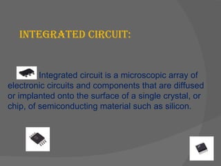
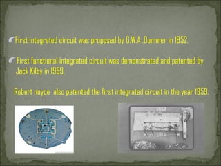
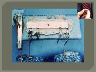
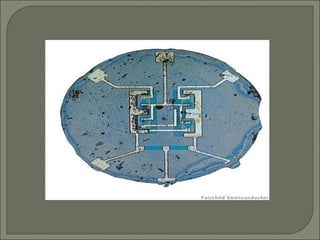
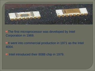

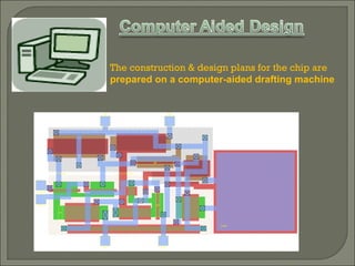
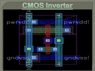
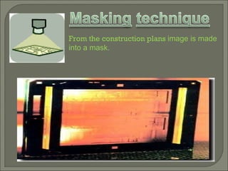
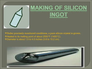
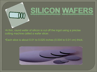
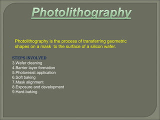
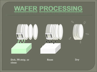
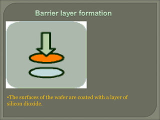
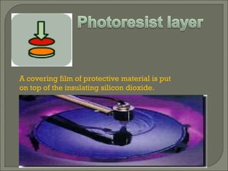
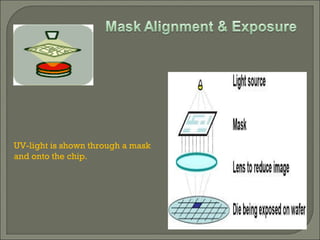
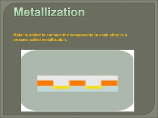
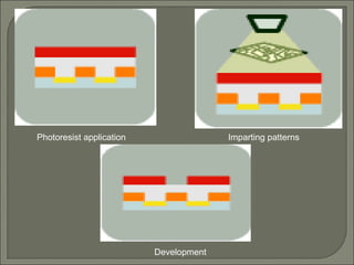
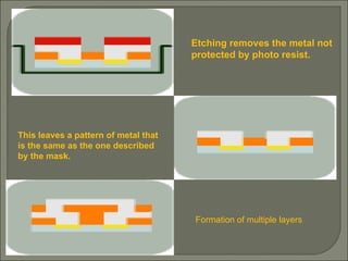
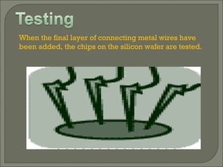
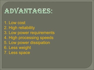
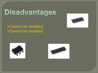


Integrated circuits (ICs) are microscopic arrays of electronic components on a silicon chip, first proposed in 1952 and developed commercially by Intel in the 1970s. The fabrication process involves multiple steps, including wafer slicing, photolithography, and metallization. ICs offer advantages such as low cost and high reliability, but they are not modifiable or repairable.

![ppt on IC [Integrated Circuit]](https://cdn.slidesharecdn.com/ss_thumbnails/1-171227170055-thumbnail.jpg?width=640&height=640&fit=bounds)


