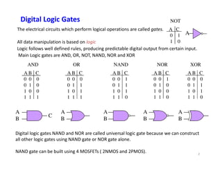
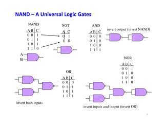
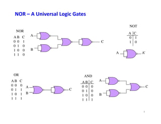
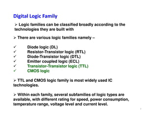
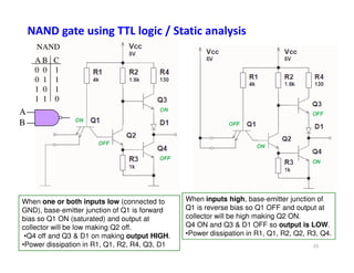
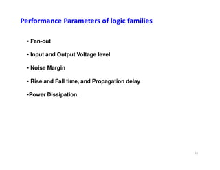
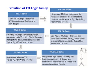
Digital logic gates called NAND and NOR are considered universal logic gates because all other logic gates can be constructed using only NAND gates or only NOR gates. Transistor-Transistor Logic (TTL) is one of the most widely used integrated circuit logic families. TTL uses a multi-emitter input transistor and a totem-pole output stage to provide a variable output resistance and achieve high noise immunity. Key parameters for logic families include input/output voltage levels, propagation delay, power dissipation, and noise margins.
it covers topics Introduction
Classification of Logic Families
Important point
Level of Integration
Specification of Digital ICs
TTL Circuit
TTL NAND Gates
MOS/CMOS Circuits
CMOS NAND Gate
ECL Circuit
Comparison
Numbers of Digital ICs
The following presentation is a part of the level 4 module -- Digital Logic and Signal Principles. This resources is a part of the 2009/2010 Engineering (foundation degree, BEng and HN) courses from University of Wales Newport (course codes H101, H691, H620, HH37 and 001H). This resource is a part of the core modules for the full time 1st year undergraduate programme.
The BEng & Foundation Degrees and HNC/D in Engineering are designed to meet the needs of employers by placing the emphasis on the theoretical, practical and vocational aspects of engineering within the workplace and beyond. Engineering is becoming more high profile, and therefore more in demand as a skill set, in today’s high-tech world. This course has been designed to provide you with knowledge, skills and practical experience encountered in everyday engineering environments.
Immunizing Image Classifiers Against Localized Adversary Attacksgerogepatton
This paper addresses the vulnerability of deep learning models, particularly convolutional neural networks
(CNN)s, to adversarial attacks and presents a proactive training technique designed to counter them. We
introduce a novel volumization algorithm, which transforms 2D images into 3D volumetric representations.
When combined with 3D convolution and deep curriculum learning optimization (CLO), itsignificantly improves
the immunity of models against localized universal attacks by up to 40%. We evaluate our proposed approach
using contemporary CNN architectures and the modified Canadian Institute for Advanced Research (CIFAR-10
and CIFAR-100) and ImageNet Large Scale Visual Recognition Challenge (ILSVRC12) datasets, showcasing
accuracy improvements over previous techniques. The results indicate that the combination of the volumetric
input and curriculum learning holds significant promise for mitigating adversarial attacks without necessitating
adversary training.
Final project report on grocery store management system..pdfKamal Acharya
In today’s fast-changing business environment, it’s extremely important to be able to respond to client needs in the most effective and timely manner. If your customers wish to see your business online and have instant access to your products or services.
Online Grocery Store is an e-commerce website, which retails various grocery products. This project allows viewing various products available enables registered users to purchase desired products instantly using Paytm, UPI payment processor (Instant Pay) and also can place order by using Cash on Delivery (Pay Later) option. This project provides an easy access to Administrators and Managers to view orders placed using Pay Later and Instant Pay options.
In order to develop an e-commerce website, a number of Technologies must be studied and understood. These include multi-tiered architecture, server and client-side scripting techniques, implementation technologies, programming language (such as PHP, HTML, CSS, JavaScript) and MySQL relational databases. This is a project with the objective to develop a basic website where a consumer is provided with a shopping cart website and also to know about the technologies used to develop such a website.
This document will discuss each of the underlying technologies to create and implement an e- commerce website.
Overview of the fundamental roles in Hydropower generation and the components involved in wider Electrical Engineering.
This paper presents the design and construction of hydroelectric dams from the hydrologist’s survey of the valley before construction, all aspects and involved disciplines, fluid dynamics, structural engineering, generation and mains frequency regulation to the very transmission of power through the network in the United Kingdom.
Author: Robbie Edward Sayers
Collaborators and co editors: Charlie Sims and Connor Healey.
(C) 2024 Robbie E. Sayers
CFD Simulation of By-pass Flow in a HRSG module by R&R Consult.pptxR&R Consult
CFD analysis is incredibly effective at solving mysteries and improving the performance of complex systems!
Here's a great example: At a large natural gas-fired power plant, where they use waste heat to generate steam and energy, they were puzzled that their boiler wasn't producing as much steam as expected.
R&R and Tetra Engineering Group Inc. were asked to solve the issue with reduced steam production.
An inspection had shown that a significant amount of hot flue gas was bypassing the boiler tubes, where the heat was supposed to be transferred.
R&R Consult conducted a CFD analysis, which revealed that 6.3% of the flue gas was bypassing the boiler tubes without transferring heat. The analysis also showed that the flue gas was instead being directed along the sides of the boiler and between the modules that were supposed to capture the heat. This was the cause of the reduced performance.
Based on our results, Tetra Engineering installed covering plates to reduce the bypass flow. This improved the boiler's performance and increased electricity production.
It is always satisfying when we can help solve complex challenges like this. Do your systems also need a check-up or optimization? Give us a call!
Work done in cooperation with James Malloy and David Moelling from Tetra Engineering.
More examples of our work https://www.r-r-consult.dk/en/cases-en/
NO1 Uk best vashikaran specialist in delhi vashikaran baba near me online vas...Amil Baba Dawood bangali
Contact with Dawood Bhai Just call on +92322-6382012 and we'll help you. We'll solve all your problems within 12 to 24 hours and with 101% guarantee and with astrology systematic. If you want to take any personal or professional advice then also you can call us on +92322-6382012 , ONLINE LOVE PROBLEM & Other all types of Daily Life Problem's.Then CALL or WHATSAPP us on +92322-6382012 and Get all these problems solutions here by Amil Baba DAWOOD BANGALI
#vashikaranspecialist #astrologer #palmistry #amliyaat #taweez #manpasandshadi #horoscope #spiritual #lovelife #lovespell #marriagespell#aamilbabainpakistan #amilbabainkarachi #powerfullblackmagicspell #kalajadumantarspecialist #realamilbaba #AmilbabainPakistan #astrologerincanada #astrologerindubai #lovespellsmaster #kalajaduspecialist #lovespellsthatwork #aamilbabainlahore#blackmagicformarriage #aamilbaba #kalajadu #kalailam #taweez #wazifaexpert #jadumantar #vashikaranspecialist #astrologer #palmistry #amliyaat #taweez #manpasandshadi #horoscope #spiritual #lovelife #lovespell #marriagespell#aamilbabainpakistan #amilbabainkarachi #powerfullblackmagicspell #kalajadumantarspecialist #realamilbaba #AmilbabainPakistan #astrologerincanada #astrologerindubai #lovespellsmaster #kalajaduspecialist #lovespellsthatwork #aamilbabainlahore #blackmagicforlove #blackmagicformarriage #aamilbaba #kalajadu #kalailam #taweez #wazifaexpert #jadumantar #vashikaranspecialist #astrologer #palmistry #amliyaat #taweez #manpasandshadi #horoscope #spiritual #lovelife #lovespell #marriagespell#aamilbabainpakistan #amilbabainkarachi #powerfullblackmagicspell #kalajadumantarspecialist #realamilbaba #AmilbabainPakistan #astrologerincanada #astrologerindubai #lovespellsmaster #kalajaduspecialist #lovespellsthatwork #aamilbabainlahore #Amilbabainuk #amilbabainspain #amilbabaindubai #Amilbabainnorway #amilbabainkrachi #amilbabainlahore #amilbabaingujranwalan #amilbabainislamabad
1. Analog & Digital Electronics
Course No: PH-218
Lec-28: Logic Gates & Family
Course Instructor:
Course Instructor:
Dr. A. P. VAJPEYI
Department of Physics,
Indian Institute of Technology Guwahati, India 1
2. Digital Logic Gates
The electrical circuits which perform logical operations are called gates.
All data manipulation is based on logic
Logic follows well defined rules, producing predictable digital output from certain input.
Main Logic gates are AND, OR, NOT, NAND, NOR and XOR
A B C
0 0 0
0 1 0
AND
A B C
0 0 0
0 1 1
OR
A B C
0 0 0
0 1 1
XOR
A B C
0 0 1
0 1 1
NAND
A B C
0 0 1
0 1 0
NOR
A
A C
0 1
1 0
NOT
0 1 0
1 0 0
1 1 1
A
B
C
0 1 1
1 0 1
1 1 1
A
B
0 1 1
1 0 1
1 1 0
A
B
0 1 1
1 0 1
1 1 0
A
B
0 1 0
1 0 0
1 1 0
A
B
Digital logic gates NAND and NOR are called universal logic gate because we can construct
all other logic gates using NAND gate or NOR gate alone.
NAND gate can be built using 4 MOSFETs ( 2NMOS and 2PMOS). 2
3. A B C
0 0 1
0 1 1
1 0 1
1 1 0
NAND
A
B
A C
0 1
1 0
NOT
A B C
0 0 0
0 1 0
1 0 0
1 1 1
AND
A B C
NOR
invert output (invert NAND)
NAND – A Universal Logic Gates
A B C
0 0 0
0 1 1
1 0 1
1 1 1
OR
A B C
0 0 1
0 1 0
1 0 0
1 1 0
invert both inputs
invert inputs and output (invert OR)
3
4. NOR – A Universal Logic Gates
A A’
A C
0 1
1 0
NOT
A
B
C
A B C
0 0 1
0 1 0
1 0 0
1 1 0
NOR
A
B
C
A B C
0 0 0
0 1 0
1 0 0
1 1 1
AND
B
C
A
A B C
0 0 0
0 1 1
1 0 1
1 1 1
OR
4
5. • XOR = (A NAND B) AND (A OR B)
• And this you already know you can make from composite NAND gates
A
B
C
XOR –Logic Gates
• And this you already know you can make from composite NAND gates
(though requiring 6 total)
• Then, obviously, XNOR is the inverse of XOR
– so just stick an inverter on the output of XOR
Exclusive OR operator: operating on two variables
A and B is true if A or B is a 1, but not when both A and B are 1, i.e. it excludes both
A and B being a 1; symbol ⊕
5
6. Logic Family / Level Of Integration
Scheme # gates / chip
Small Scale Integration (SSI) 12
Medium Scale Integration (MSI) 12 - 99
Large Scale Integration (LSI) 1000
Very large Scale Integration (VLSI) 10k
Ultra large Scale Integration (ULSI) 100k
Note: Ratio gate count/transistor count is roughly 1/10
IC logic gates fall under SSI, combinational logic circuits fall under MSI, and
Microprocessor system come under LSI and VLSI.
Ultra large Scale Integration (ULSI) 100k
Giga Scale Integration (GSI) 1Meg
6
7. Digital Logic Family
There are various logic families namely –
Diode logic (DL)
Resistor-Transistor logic (RTL)
Diode-Transistor logic (DTL)
Emitter coupled logic (ECL)
Logic families can be classified broadly according to the
technologies they are built with
Emitter coupled logic (ECL)
Transistor-Transistor logic (TTL)
CMOS logic
TTL and CMOS logic family is most widely used IC
technologies.
Within each family, several subfamilies of logic types are
available, with different rating for speed, power consumption,
temperature range, voltage level and current level.
7
8. Nomenclature of Logic family
The different manufacturers of digital logic ICs have standardized a
numbering scheme so that basic part number will be same regardless of
the manufacturer.
The prefix of the part number represents the manufacturer code and the
suffix at the middle denotes the subfamily of the ICs and suffix at the end
denotes the packaging type.
For example: If the part number is S74F08N. The 7408 is the basic number
used by all manufacturer for quad AND gate. The S prefix is the
manufacture’s code for Signetics, F stands for FAST TTL subfamily, and the
N suffix at the end is used to specify the plastic dual in line packaging
Suffix used for packaging:
N - Plastic dual in line package
W - Ceramic flat pack
D - Surface mounted plastic package
Prefix used for manufacturers:
S - Signetics
SN - Texas Instruments
DM - National Semiconductor
Suffix used for subfamily:
74H04 - High-speed
74L045- Low-Power
74S04 - Uses a Schottky Diode
74ALS04 - Advanced low power Schottky
8
9. Diode Logic Family
In diode logic family, all the logic is implemented using diodes and resistors.
One basic thing about the diode, is that diode needs to be forward biased to conduct.
X Y Z
0 0 0
0 1 1
1 0 1
OR
Diode Logic suffers from voltage degradation from one stage to the next.
Diode Logic only permits OR and AND functions, cannot perform a NOT function.
Diode Logic is used extensively but not in integrated circuits
1 0 1
1 1 1
How to build AND gate using Diode logic?
9
10. Resistor Transistor Logic (RTL) Family
In RTL (resistor transistor logic), all the logic are implemented using resistors and
transistors. One basic thing about the transistor (NPN), is that HIGH at input causes
output to be LOW (i.e. like a inverter).
X Y Z
0 0 1
0 1 0
1 0 0
NOR
A
B
NOR gate using RTL
1 0 0
1 1 0
RTL draw a significant amount of current
from the power supply for each gate.
Another limitation is that RTL gates
cannot switch at the high speeds used by
today's computers, although they are still
useful in slower applications
10
11. Transistor Transistor Logic (TTL) Family
One basic function of TTL IC is as a complimenting switch or inverter.
When Vin equals 1 (+5V), the transistor is turned on (saturation) and Vout equals 0 (0V).
When Vin equals 0 (0V), the transistor is turned off and Vout equals 1 (5V), assuming RL RC
RC
IC
+5V
)
R
(R
R
V
V
L
C
L
CC
out
+
=
Thus level 1 of inverter output is very much
RB
RC
RE
IB
IE
B
E
C
RL
Vin
Vout
Thus level 1 of inverter output is very much
dependent on RL , which can typically vary
by factor of 10. Thus we need very small RC
compared to RL i.e. RL RC .
But when transistor is saturated (Vout = 0V),
IC will be very large if RC is very small.
Thus we need large RC when transistor is in
satuaration and small RC when transistor is
off.
The idea of variable RC is accommodated by TTL IC. 11
12. Transistor Transistor Logic (TTL) Family
Q3 is cutoff (act like a high RC ) when output
transistor Q4 is saturated and Q3 is
saturated (act like a low RC ) when output
transistor Q4 is cutoff . Thus one transistor is
ON at one time.
The combination of Q3 and Q4 is called
The idea of variable RC is accommodated by TTL IC. It uses another transistor Q3 in place of
RC to act like a varying resistance.
The combination of Q3 and Q4 is called
totem pole arrangement.
Q1 is called input transistor, which is multi-
emitter transistor, that drive transistor Q2
which is used to control Q3 and Q4.
Diode D1 and D2 is used to protect Q1 from
unwanted negative voltages and diode D3
ensures when Q4 is ON, Q3 is OFF.
Multi-emitter input transistor is a striking feature of TTL logic family. 12
13. Transistor Transistor Logic - Dual In Line Packaging (DIP)
Dual In Line package (DIP) is the most common pin layout for integrated circuits. The pins
are aligned in two straight lines, one on each side of the IC.
IC 7400
13
14. Transistor Transistor Logic - Dual In Line Packaging (DIP)
IC 7404 IC 7408
Some common digital ICs used in labs are: IC7400 (Quad NAND gate), IC 7404 ( hex
inverter), IC 7408 (quad AND gate) and IC7402 (quad NOR gates).
IC 7402
14
15. NAND gate using TTL logic / Static analysis
A B C
0 0 1
0 1 1
1 0 1
1 1 0
NAND
A
B
When one or both inputs low (connected to
GND), base-emitter junction of Q1 is forward
bias so Q1 ON (saturated) and output at
collector will be low making Q2 off.
•Q4 off and Q3 D1 on making output HIGH.
•Power dissipation in R1, Q1, R2, R4, Q3, D1
When inputs high, base-emitter junction of
Q1 is reverse bias so Q1 OFF and output at
collector will be high making Q2 ON.
Q4 ON and Q3 D1 OFF so output is LOW.
•Power dissipation in R1, Q1, R2, Q2, R3, Q4.
15
16. • Fan-out
• Input and Output Voltage level
• Noise Margin
• Rise and Fall time, and Propagation delay
Performance Parameters of logic families
•Power Dissipation.
16
17. Input / Output Current and Fan-out
The fan-out of a subfamily is defined as the number
of gate inputs of the same subfamily that can be
connected to a single output without exceeding the
current ratings of the gate.
A typical fan-out for most TTL subfamilies is 10.
The fan-out really depends on the amount
of electric current a gate can source or
sink while driving other gates. The effects
of loading a logic gate output with more
than its rated fan-out will degrade the
performance of the circuit.
The gate delay increases with increase in
fan-out.
17
18. Input / Output Current and Fan-out
To determine fan-out, one must know how much input current gate load
draws (Iin) and how much output current the driving gate can supply (Io).
The output current capability for the HIGH condition is abbreviated IoH
and is called source current. IoH for the 7400 is -400uA maximum. (- sign
shows current is leaving the gate)
The input current required under HIGH condition is abbreviated IIH and for
74xx subfamily is equal to 40uA maximum. Fan-out = 400/40 = 10
For the LOW condition, the maximum output current for the 74xx
subfamily is 16mA, and the input requirement is -1.6mA maximum.
The fan-out is usually same for both the HIGH and LOW conditions for
74xx subfamily; if not, we use the lower of the two.
Because a LOW output level is close to 0V, the current actually flows into
the output terminal and sinks down to ground. This is called sink current.
18
19. Input / Output Voltage for TTL family
There is a limit on voltage until it is considered HIGH. As we draw more and
more current out of the HIGH level output, the output voltage drops lower and
lower, until finally it will not be recognized as a HIGH level anymore by the
other TTL gates that it is feeding.
•VOHmin : The minimum output voltage
in HIGH state (logic '1') = 2.4V for TTL
•VOLmax : The maximum output voltage
in LOW state (logic '0') = 0.4V for TTL
•VIHmin : The minimum input voltage
guaranteed to be recognised as logic 1.
VIHmin = 2 V for TTL
VILmax : The maximum input voltage
guaranteed to be recognised as logic 0.
VILmax = 0.8 V for TTL
19
20. Noise Margin for TTL family
Noise-Margin measures how much external electrical noise a gate can
withstand before producing an incorrect output. TTL will take anything
below about 0.8 volt as a 0, and anything above about 2 volts as a high.
LNM (Low noise margin): The largest
noise amplitude that is guaranteed not to
change the output voltage level when
superimposed on the input voltage of the
logic gate (when this voltage is in the LOW).
LNM=VILmax-VOLmax = 0.8V-0.4V = 0.4V
HNM (High noise margin): The largest
noise amplitude that is guaranteed not to
change the output voltage level if
superimposed on the input voltage of the
logic gate (when this voltage is in the HIGH).
HNM=VOHmin-VIHmin = 2.4-2.0 = 0.4V
20
21. Switching time and Propagation delay time
The rise time (tr) is the length of time it takes for a pulse to rise from its
10% point up to its 90% point.
The fall time (tf) is the length of time it takes for a pulse to fall from its
90% point to its 10% point.
The propagation delay time is
define as the average of low
to- high (tPLH) propagation
delay time and the high-to-low
(tPHL) propagation delay time.
propagation delay time
tP = (tPLH + tPHL) / 2
The propagation delay time is
directly proportional to the
switching time and increases
as the Fan-out increases.
21
22. Estimation of propagation delay time
The propagation delay time is due to limitations in transistor switching
speeds caused by undesirable internal capacitive stored charges.
The two modes of capacitive charging/discharging that contribute to
propagation delay
22
23. Estimation of propagation delay time
To calculate delay, we consider transistor as a switch
dt
dV
C
I = V
dV
C
I
dV
C
dt R
=
=
=
=
= ∫
V
V
p
V
V
RC
V
dV
RC
t
o
1
0
1 ln
t
-
t
1
∫ o
V V
V
o
For fall delay tphl, V0=Vcc, V1=Vcc/2 tphl = 0.69RnCL tplh = 0.69RPCL
Total propagation delay time: tP = (tPLH + tPHL) / 2
23
24. Evolution of TTL Logic Family
TTL 74 Series
Standard TTL logic – saturated
BJT, Obsolete now, Don’t use in
new designs
TTL 74S Series
Schottky TTL logic – Deep saturation
prevented by BC Schottky Diode. Reduced
TTL 74H Series
High speed TTL logic – decrease the
resistance to lower the internal time
constant but increase in Pdis. Typical Pdis
=22mW and t = 6ns
TTL 74L Series
Low Power TTL logic – Increase the
prevented by BC Schottky Diode. Reduced
storage time delay. Practically obsolete.
Typical Pdis =20mW and t = 3ns
Low Power TTL logic – Increase the
resistance to lower the Pdis but increase
in internal time constant . Typical Pdis
=1mW and t = 35ns
TTL 74ALS Series
Low power, high speed Schottky TTL
logic-Innovations in IC design and
fabrication. Improvement in speed and
power dissipation. Popular.
TTL 74LS Series
Low power Schottky TTL.
Typical Pdis =2mW and t = 10ns