Downloaded 481 times
![[1] Ned Mohan, Undeland and Robbin, ‘Power Electronics: Converters,
Application and Design’, John Wiley and sons Inc., Newyork,2006.
[2] Rashid M.H., ‘Power Electronics- Circuits, Device and Applications’,
Prentice Hall India, New Delhi, 2009.
[3] Datasheets
1N5820 http://www.farnell.com/datasheets/107972.pdf
IRFZ14 http://www.irf.com/product-info/datasheets/data/irfz14.pdf
Capacitor http://www.farnell.com/datasheets/1558295.pdf
11Design of Buck converter](https://image.slidesharecdn.com/presentation1-151112132059-lva1-app6891/75/Design-of-Buck-Converter-11-2048.jpg)


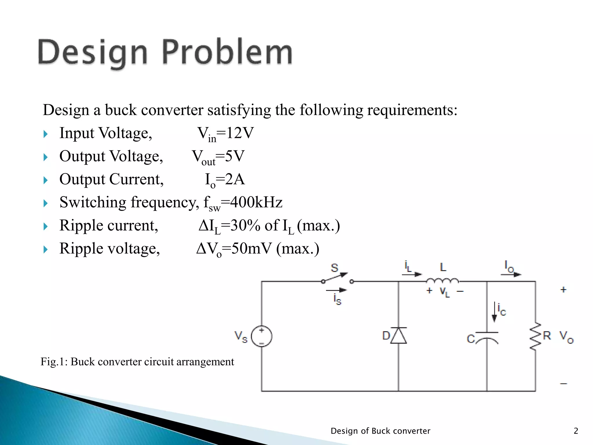
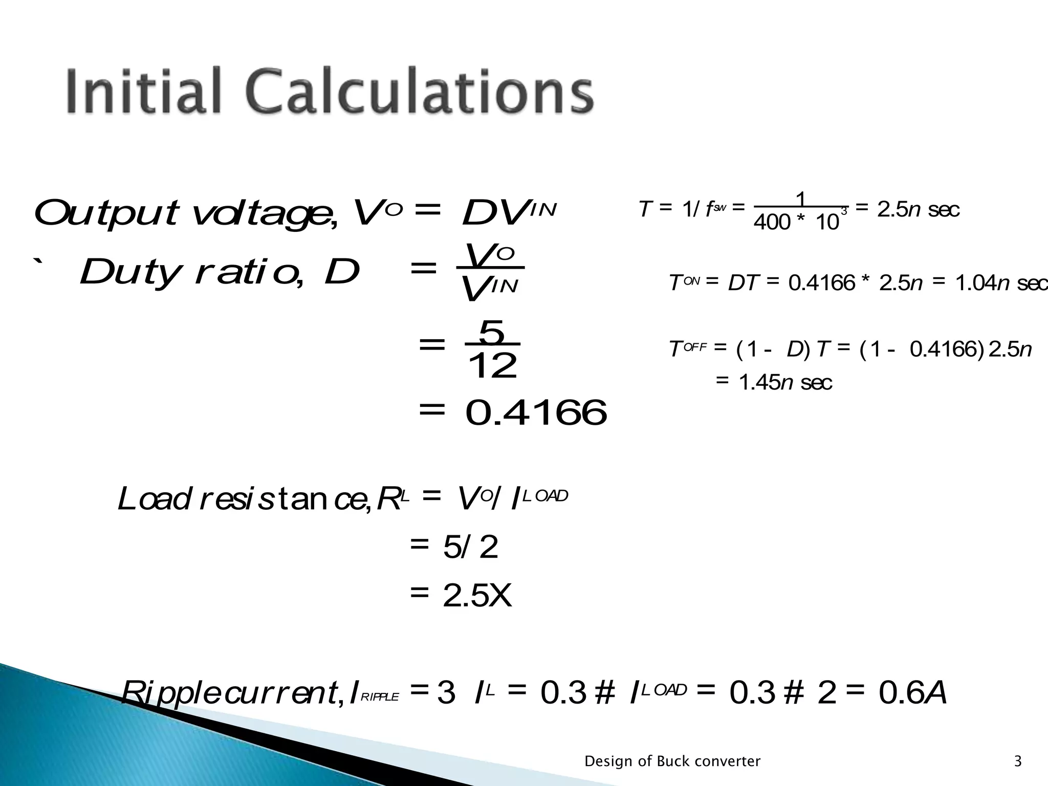
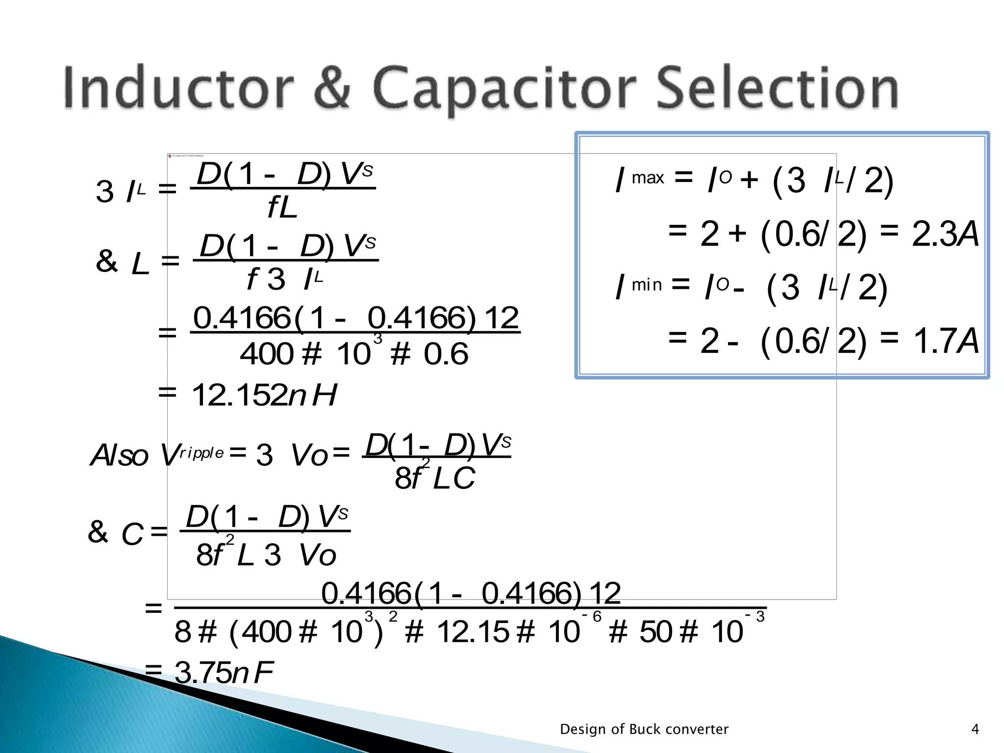
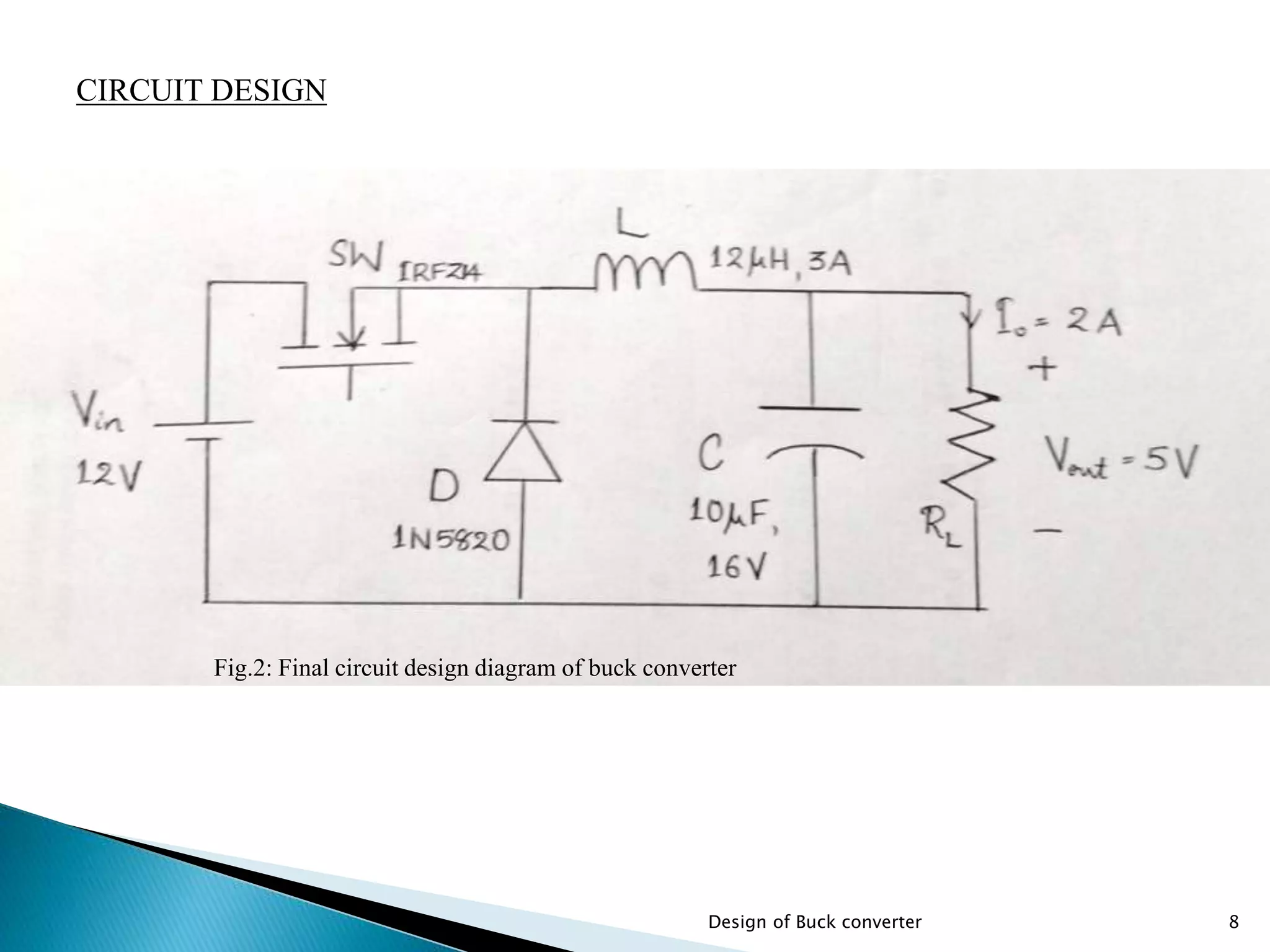
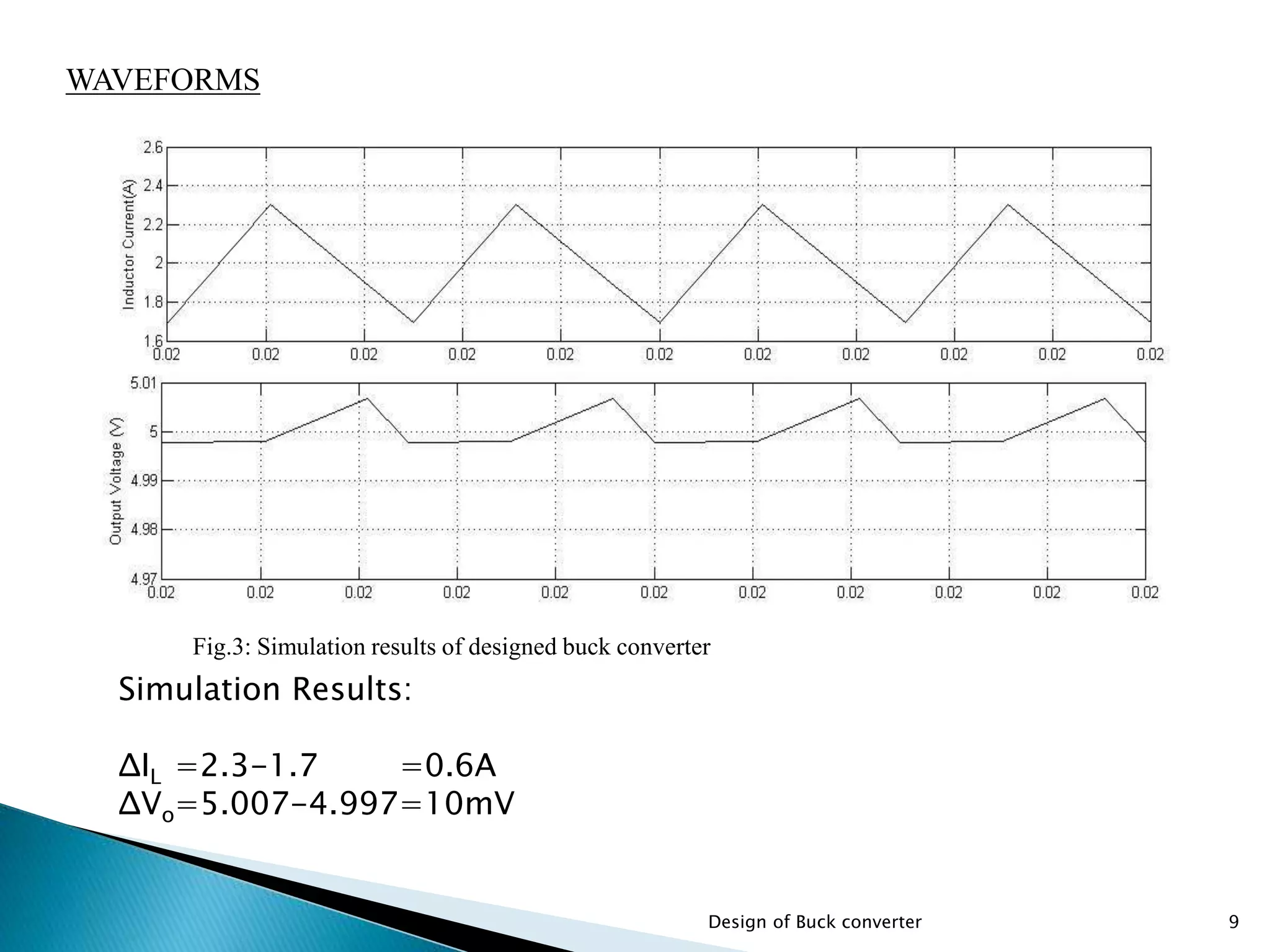
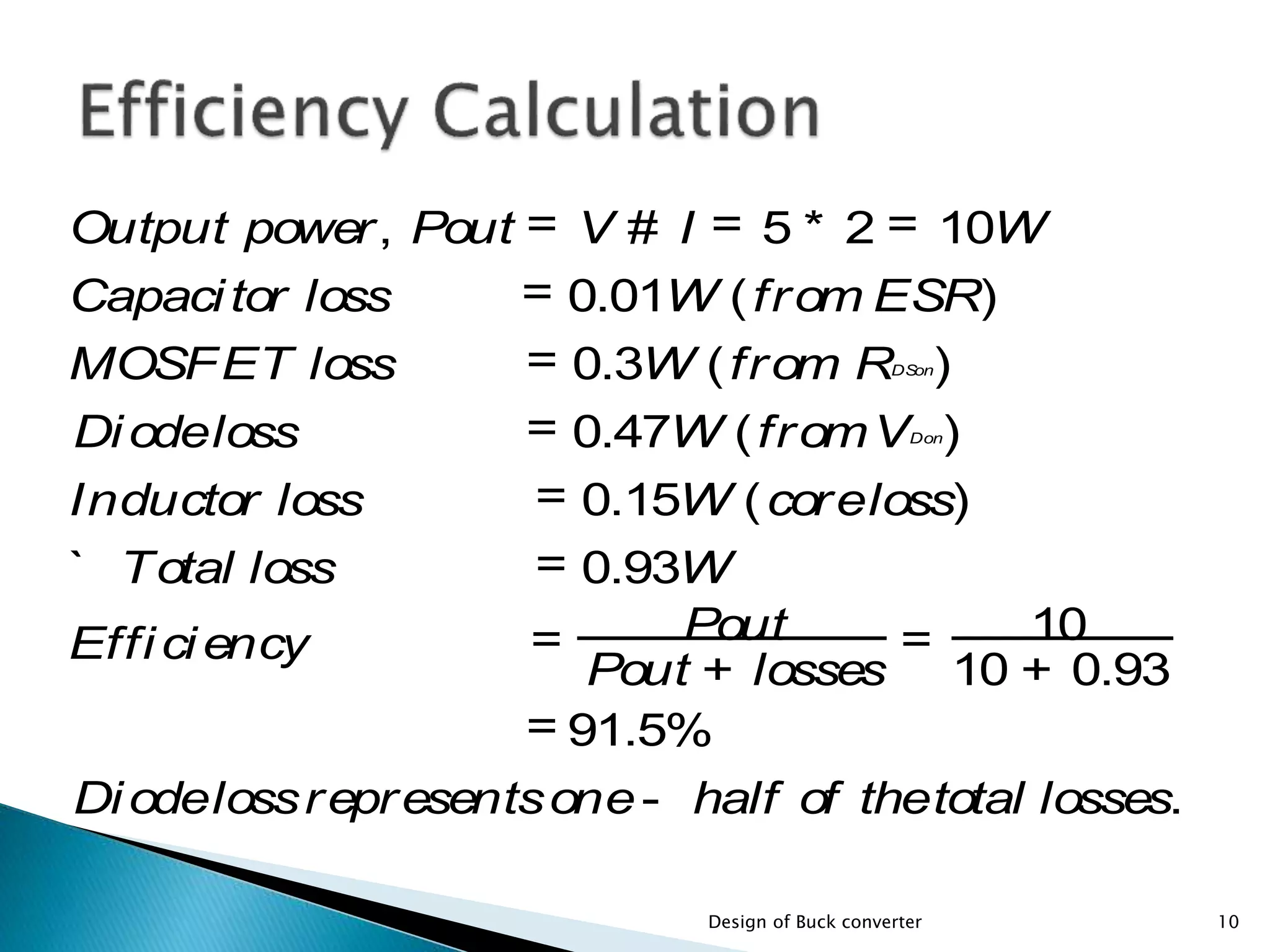
The document presents the design specifications and calculations for a buck converter with an input voltage of 12V and an output voltage of 5V, capable of delivering a current of 2A. It includes detailed calculations for components such as inductance and capacitance, selection of components like a diode and a MOSFET, as well as the simulation results indicating an efficiency of 91.5% and the total loss of 0.93W. The design adheres to the given requirements, as all calculated component values exceed critical specifications.


