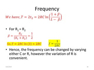
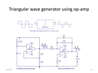
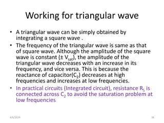
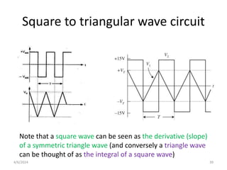
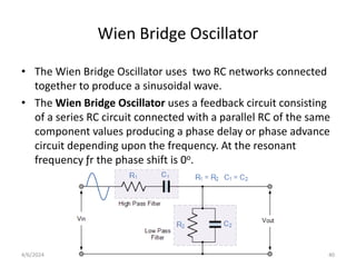
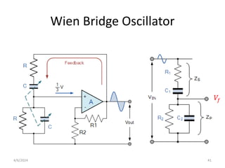
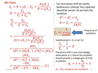
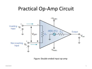
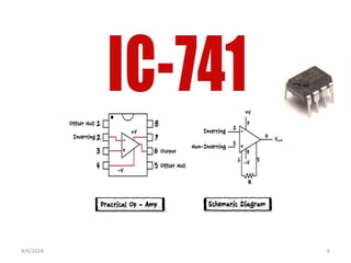
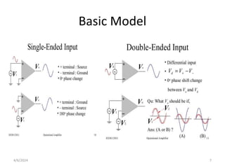
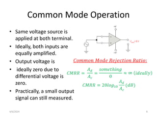
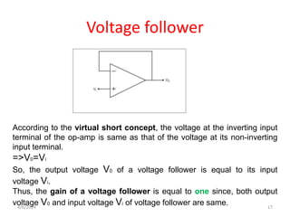
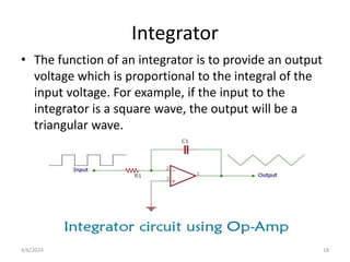
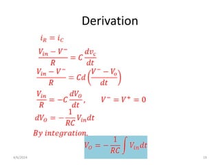
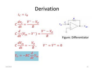
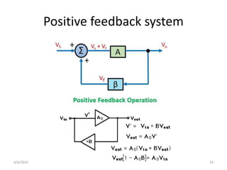
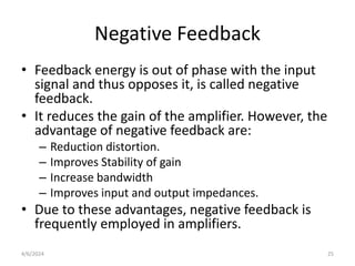
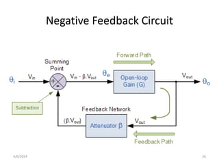
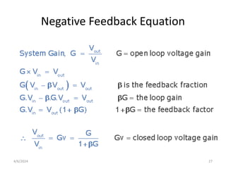
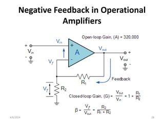
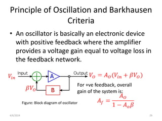
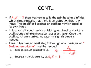
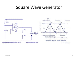
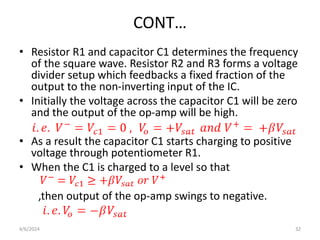
Contents
4.1 Basic model: virtual ground concept,
inverting amplifier, non-inverting amplifier,
integrator, differentiator, summing amplifier
and their applications.
4.2 Basic feedback theory, positive and negative
feedback, concept of stability, oscillator
4.3 Waveform generator using op-amp for
Square wave, Triangular wave Wien bridge
oscillator for sinusoidal waveform
4/6/2024 1
Introduction
• Operational Amplifier, also called as an Op-Amp, is an integrated
circuit, which can be used to perform various linear, non-linear, and
mathematical operations.
• An op-amp is a direct coupled high gain amplifier. We can operate
op-amp both with AC and DC signals.
• An Operational Amplifier, or op-amp, is fundamentally a voltage
amplifying device designed to be used with external feedback
components such as resistors and capacitors between its output
and input terminals.
• These feedback components determine the resulting function or
“operation” of the amplifier and by virtue of the different feedback
configurations whether resistive, capacitive or both, the amplifier
can perform a variety of different operations, giving rise to its name
of “Operational Amplifier”.
4/6/2024 2
CONT…
• An Operational Amplifier is basically a three-
terminal device which consists of two high
impedance inputs. One of the inputs is called
the Inverting Input, marked with a negative or
“minus” sign, ( – ). The other input is called
the Non-inverting Input, marked with a positive
or “plus” sign ( + ).
• An Operational Amplifiers gain is commonly
known as the Open Loop Differential Gain, and is
given the symbol (Ao).
4/6/2024 3
Ideal and Practical Op- Amp
Ideal Op-Amp
Practical Op-Amp
4/6/2024 4
Practical Op-Amp Circuit
Figure: Double ended input op-amp
4/6/2024 5
4/6/2024 6
Basic Model
• Double-ended Input
4/6/2024 7
Common Mode Operation
• Same voltage source is
applied at both terminal.
• Ideally, both inputs are
equally amplified.
• Output voltage is
• ideally zero due to
differential voltage is
zero.
• Practically, a small output
signal can still measured.
4/6/2024 8
Ideal Op-Amp Characteristics
• Open Loop Gain (without any feedback path), (Aol) Infinite
– Aol=vo/(v1-v2)
• Input impedance, (ZIN) Infinite
• Output impedance, (ZOUT)  Zero
• Virtual ground or short between the input terminals.
• Bandwidth, (BW): Infinite
• Offset Voltage, (VOf)  Zero
– This refers to the situation where the same signal is
applied to both inputs. For an ideal differential amplifier
no output should be seen at the output under these
circumstances, however the amplifier will never be
perfect.
• (Common mode rejection): CMMR= Ad/Ac = (infinite)
• Infinite slew rate, so that output voltage changes occur
simultaneously with input voltage.
4/6/2024 9
Virtual Ground
• .
4/6/2024 10
Inverting Amplifier
• The closed loop gain, G is given
by,
• Current flowing through Rin
• Current flowing through Rf
• We know, iin = if due to infinite
input impedance
• From equation (2) and (3)
• -ve sign shows input and output
signals are 180 out of phase,
so called inverting amplifier.
if
iin
• Non-inverting terminal is grounded,
where as Rin connected to the input
signal (Vin) to the inverting input.
• A feedback register Rf has been
connected from the output to the
inverting input.
4/6/2024 11
Non-Inverting Amplifier
• We know,
i1 = if
Derive yourself
4/6/2024 12
Adder or Summing Amplifier
• We know,
• If we have
4/6/2024 13
Differential Amplifier (Subtractor)
• Differential amplifier
amplifies the voltage
difference present on its
inverting and non-inverting
inputs.
4/6/2024 14
Derivation
• Apply superposition theorem using the following steps
Step 1
• Calculate the output voltage V01 by considering only V1
• For this, eliminate V2 by making it short circuit. Then we obtain
the modified circuit diagram as shown in the following figure −
4/6/2024 15
CONT…
Step 2:
• In this step, let us find the output voltage, V02 by considering only V2.
• eliminate V1 by making it short circuit. The modified circuit diagram is shown
in the following figure.
Step 3:
•we will obtain the output voltage Vo of
the subtractor circuit by adding the
output voltages obtained in Step1 and
Step2. Mathematically, it can be written
as:
4/6/2024 16
Voltage follower
According to the virtual short concept, the voltage at the inverting input
terminal of the op-amp is same as that of the voltage at its non-inverting
input terminal.
=>V0=Vi
So, the output voltage V0 of a voltage follower is equal to its input
voltage Vi.
Thus, the gain of a voltage follower is equal to one since, both output
voltage V0 and input voltage Vi of voltage follower are same.
4/6/2024 17
Integrator
• The function of an integrator is to provide an output
voltage which is proportional to the integral of the
input voltage. For example, if the input to the
integrator is a square wave, the output will be a
triangular wave.
4/6/2024 18
Derivation
4/6/2024 19
Differentiator
• Its function is to provide an output voltage
which is proportional to the rate of change of
the input voltage.
• Differentiator circuit can be obtained by
interchanging the resistor and capacitor of the
integrator circuit.
• If the input to the differentiator is a triangular
wave, the output will be a square wave.
4/6/2024 20
Derivation
Figure: Differentiator
4/6/2024 21
4.2 Feedback Theory
• The process of injecting a fraction of output
energy of some device back to the input is known
as feedback.
• It has been found very useful in reducing noise in
amplifier and making amplifier operation stable.
• Depending upon whether the feedback energy
aids or oppose the input signal, there are two
basic types of feedback in amplifiers.
1. Positive feedback
2. Negative feedback
4/6/2024 22
Positive Feedback
• When the feedback energy (voltage or current) is
in phase with the input signal and thus aids it,
called positive feedback.
• Positive feedback increases the gain of the
amplifier. However, it has the disadvantage of
increased distortion and instability.
• Therefore, positive feedback is seldom employed
in amplifiers.
• One important use of positive feedback is in
oscillator.
4/6/2024 23
Positive feedback system
24
4/6/2024
Negative Feedback
• Feedback energy is out of phase with the input
signal and thus opposes it, is called negative
feedback.
• It reduces the gain of the amplifier. However, the
advantage of negative feedback are:
– Reduction distortion.
– Improves Stability of gain
– Increase bandwidth
– Improves input and output impedances.
• Due to these advantages, negative feedback is
frequently employed in amplifiers.
4/6/2024 25
Negative Feedback Circuit
26
4/6/2024
Negative Feedback Equation
27
4/6/2024
Negative Feedback in Operational
Amplifiers
28
4/6/2024
Principle of Oscillation and Barkhausen
Criteria
• An oscillator is basically an electronic device
with positive feedback where the amplifier
provides a voltage gain equal to voltage loss in
the feedback network.
Figure: Block diagram of oscillator
For +ve feedback, overall
gain of the system is:
4/6/2024 29
CONT…
• If then mathematically the gain becomes infinite
which simply means that there is an output without any
input. The amplifier becomes an oscillator which supplies
its own input.
• In fact, circuit needs only a quick trigger signal to start the
oscillations and even noise can act as a trigger. Once the
oscillators have started, no external signal source is
needed.
• Thus to become an oscillator, following two criteria called “
Barkhausen criteria” must be needed:
1. Feedback must be positive i.e.
2. Loop gain should be unity i.e.
4/6/2024 30
Square Wave Generator
4/6/2024 31
CONT…
• Resistor R1 and capacitor C1 determines the frequency
of the square wave. Resistor R2 and R3 forms a voltage
divider setup which feedbacks a fixed fraction of the
output to the non-inverting input of the IC.
• Initially the voltage across the capacitor C1 will be zero
and the output of the op-amp will be high.
• As a result the capacitor C1 starts charging to positive
voltage through potentiometer R1.
• When the C1 is charged to a level so that
,then output of the op-amp swings to negative.
4/6/2024 32
CONT…
• When Vo= -Vsat and Vf or V+=-βVsat
• The capacitor quickly discharges through R1 and then
starts charging to negative voltage from +βVsat to - Vsat .
• After certain time, When V-=Vc1  -βVsat more negative
than that of the non-inverting pin, the output of the
op-amp swings back to positive voltage. i.e. Vout= +Vsat
• Now the capacitor again starts charging to positive
voltage from –βVsat to +βVsat .
• This cycle is repeated endlessly and the result will a
continuous square wave swinging between +Vsat and
–Vsat at the output.
4/6/2024 33
Determination of Time Period/Frequency
• Let, the time taken to charge the capacitor from –βVsat to
+βVsat be t1 (which is equal to time taken t2). Then the period
of square wave is:
T= t1 + t2= 2t1
• For charging of capacitor,
Vc(t1)=Vapp – [Vapp – Vc(initial)] e-t/RC ….(1)
Where
Vapp= +Vsat
Vc(initial)= -Vsat
Vc(t1)= +Vsat
substituting these values in eqn (1)
4/6/2024 34
CONT…
• For charging of capacitor,
+Vsat = +Vsat – [+Vsat +Vsat] e-t1/RC ……(1)
• Vsat(1 - )= +Vsat [1 +] e-t1/RC
• similarly,
4/6/2024 35
Frequency
• For R1 = R2
• Hence, the frequency can be changed by varying
either C or R, however the variation of R is
convenient.
4/6/2024 36
Triangular wave generator using op-amp
37
4/6/2024
Working for triangular wave
• A triangular wave can be simply obtained by
integrating a square wave .
• The frequency of the triangular wave is same as that
of square wave. Although the amplitude of the square
wave is constant (± Vsat), the amplitude of the
triangular wave decreases with an increase in its
frequency, and vice versa. This is because the
reactance of capacitor(C2) decreases at high
frequencies and increases at low frequencies.
• In practical circuits (Integrated circuit), resistance R5 is
connected across C2 to avoid the saturation problem at
low frequencies
38
4/6/2024
Square to triangular wave circuit
Note that a square wave can be seen as the derivative (slope)
of a symmetric triangle wave (and conversely a triangle wave
can be thought of as the integral of a square wave)
39
4/6/2024
Wien Bridge Oscillator
• The Wien Bridge Oscillator uses two RC networks connected
together to produce a sinusoidal wave.
• The Wien Bridge Oscillator uses a feedback circuit consisting
of a series RC circuit connected with a parallel RC of the same
component values producing a phase delay or phase advance
circuit depending upon the frequency. At the resonant
frequency ƒr the phase shift is 0o.
40
4/6/2024
Wien Bridge Oscillator
41
4/6/2024
We have, For zero phase shift (to satisfy
barkhausen criteria), the j operator
should be vanish. So we have the
condition
Frequency of
oscillation
Substituting R = Xc in eqn (1)
The phase shift is zero and voltage
attenuation is 3. Hence the amplifier
should provide a voltage gain of 3 for
oscillation.
R1 = 2R2, condition for oscillation
4/6/2024 42
Unit 4 End
Thank You !

basic electrical and electronics engineering fundamentals of transistors biasing

  • 1.
    Contents 4.1 Basic model:virtual ground concept, inverting amplifier, non-inverting amplifier, integrator, differentiator, summing amplifier and their applications. 4.2 Basic feedback theory, positive and negative feedback, concept of stability, oscillator 4.3 Waveform generator using op-amp for Square wave, Triangular wave Wien bridge oscillator for sinusoidal waveform 4/6/2024 1
  • 2.
    Introduction • Operational Amplifier,also called as an Op-Amp, is an integrated circuit, which can be used to perform various linear, non-linear, and mathematical operations. • An op-amp is a direct coupled high gain amplifier. We can operate op-amp both with AC and DC signals. • An Operational Amplifier, or op-amp, is fundamentally a voltage amplifying device designed to be used with external feedback components such as resistors and capacitors between its output and input terminals. • These feedback components determine the resulting function or “operation” of the amplifier and by virtue of the different feedback configurations whether resistive, capacitive or both, the amplifier can perform a variety of different operations, giving rise to its name of “Operational Amplifier”. 4/6/2024 2
  • 3.
    CONT… • An OperationalAmplifier is basically a three- terminal device which consists of two high impedance inputs. One of the inputs is called the Inverting Input, marked with a negative or “minus” sign, ( – ). The other input is called the Non-inverting Input, marked with a positive or “plus” sign ( + ). • An Operational Amplifiers gain is commonly known as the Open Loop Differential Gain, and is given the symbol (Ao). 4/6/2024 3
  • 4.
    Ideal and PracticalOp- Amp Ideal Op-Amp Practical Op-Amp 4/6/2024 4
  • 5.
    Practical Op-Amp Circuit Figure:Double ended input op-amp 4/6/2024 5
  • 6.
  • 7.
  • 8.
    Common Mode Operation •Same voltage source is applied at both terminal. • Ideally, both inputs are equally amplified. • Output voltage is • ideally zero due to differential voltage is zero. • Practically, a small output signal can still measured. 4/6/2024 8
  • 9.
    Ideal Op-Amp Characteristics •Open Loop Gain (without any feedback path), (Aol) Infinite – Aol=vo/(v1-v2) • Input impedance, (ZIN) Infinite • Output impedance, (ZOUT)  Zero • Virtual ground or short between the input terminals. • Bandwidth, (BW): Infinite • Offset Voltage, (VOf)  Zero – This refers to the situation where the same signal is applied to both inputs. For an ideal differential amplifier no output should be seen at the output under these circumstances, however the amplifier will never be perfect. • (Common mode rejection): CMMR= Ad/Ac = (infinite) • Infinite slew rate, so that output voltage changes occur simultaneously with input voltage. 4/6/2024 9
  • 10.
  • 11.
    Inverting Amplifier • Theclosed loop gain, G is given by, • Current flowing through Rin • Current flowing through Rf • We know, iin = if due to infinite input impedance • From equation (2) and (3) • -ve sign shows input and output signals are 180 out of phase, so called inverting amplifier. if iin • Non-inverting terminal is grounded, where as Rin connected to the input signal (Vin) to the inverting input. • A feedback register Rf has been connected from the output to the inverting input. 4/6/2024 11
  • 12.
    Non-Inverting Amplifier • Weknow, i1 = if Derive yourself 4/6/2024 12
  • 13.
    Adder or SummingAmplifier • We know, • If we have 4/6/2024 13
  • 14.
    Differential Amplifier (Subtractor) •Differential amplifier amplifies the voltage difference present on its inverting and non-inverting inputs. 4/6/2024 14
  • 15.
    Derivation • Apply superpositiontheorem using the following steps Step 1 • Calculate the output voltage V01 by considering only V1 • For this, eliminate V2 by making it short circuit. Then we obtain the modified circuit diagram as shown in the following figure − 4/6/2024 15
  • 16.
    CONT… Step 2: • Inthis step, let us find the output voltage, V02 by considering only V2. • eliminate V1 by making it short circuit. The modified circuit diagram is shown in the following figure. Step 3: •we will obtain the output voltage Vo of the subtractor circuit by adding the output voltages obtained in Step1 and Step2. Mathematically, it can be written as: 4/6/2024 16
  • 17.
    Voltage follower According tothe virtual short concept, the voltage at the inverting input terminal of the op-amp is same as that of the voltage at its non-inverting input terminal. =>V0=Vi So, the output voltage V0 of a voltage follower is equal to its input voltage Vi. Thus, the gain of a voltage follower is equal to one since, both output voltage V0 and input voltage Vi of voltage follower are same. 4/6/2024 17
  • 18.
    Integrator • The functionof an integrator is to provide an output voltage which is proportional to the integral of the input voltage. For example, if the input to the integrator is a square wave, the output will be a triangular wave. 4/6/2024 18
  • 19.
  • 20.
    Differentiator • Its functionis to provide an output voltage which is proportional to the rate of change of the input voltage. • Differentiator circuit can be obtained by interchanging the resistor and capacitor of the integrator circuit. • If the input to the differentiator is a triangular wave, the output will be a square wave. 4/6/2024 20
  • 21.
  • 22.
    4.2 Feedback Theory •The process of injecting a fraction of output energy of some device back to the input is known as feedback. • It has been found very useful in reducing noise in amplifier and making amplifier operation stable. • Depending upon whether the feedback energy aids or oppose the input signal, there are two basic types of feedback in amplifiers. 1. Positive feedback 2. Negative feedback 4/6/2024 22
  • 23.
    Positive Feedback • Whenthe feedback energy (voltage or current) is in phase with the input signal and thus aids it, called positive feedback. • Positive feedback increases the gain of the amplifier. However, it has the disadvantage of increased distortion and instability. • Therefore, positive feedback is seldom employed in amplifiers. • One important use of positive feedback is in oscillator. 4/6/2024 23
  • 24.
  • 25.
    Negative Feedback • Feedbackenergy is out of phase with the input signal and thus opposes it, is called negative feedback. • It reduces the gain of the amplifier. However, the advantage of negative feedback are: – Reduction distortion. – Improves Stability of gain – Increase bandwidth – Improves input and output impedances. • Due to these advantages, negative feedback is frequently employed in amplifiers. 4/6/2024 25
  • 26.
  • 27.
  • 28.
    Negative Feedback inOperational Amplifiers 28 4/6/2024
  • 29.
    Principle of Oscillationand Barkhausen Criteria • An oscillator is basically an electronic device with positive feedback where the amplifier provides a voltage gain equal to voltage loss in the feedback network. Figure: Block diagram of oscillator For +ve feedback, overall gain of the system is: 4/6/2024 29
  • 30.
    CONT… • If thenmathematically the gain becomes infinite which simply means that there is an output without any input. The amplifier becomes an oscillator which supplies its own input. • In fact, circuit needs only a quick trigger signal to start the oscillations and even noise can act as a trigger. Once the oscillators have started, no external signal source is needed. • Thus to become an oscillator, following two criteria called “ Barkhausen criteria” must be needed: 1. Feedback must be positive i.e. 2. Loop gain should be unity i.e. 4/6/2024 30
  • 31.
  • 32.
    CONT… • Resistor R1and capacitor C1 determines the frequency of the square wave. Resistor R2 and R3 forms a voltage divider setup which feedbacks a fixed fraction of the output to the non-inverting input of the IC. • Initially the voltage across the capacitor C1 will be zero and the output of the op-amp will be high. • As a result the capacitor C1 starts charging to positive voltage through potentiometer R1. • When the C1 is charged to a level so that ,then output of the op-amp swings to negative. 4/6/2024 32
  • 33.
    CONT… • When Vo=-Vsat and Vf or V+=-βVsat • The capacitor quickly discharges through R1 and then starts charging to negative voltage from +βVsat to - Vsat . • After certain time, When V-=Vc1  -βVsat more negative than that of the non-inverting pin, the output of the op-amp swings back to positive voltage. i.e. Vout= +Vsat • Now the capacitor again starts charging to positive voltage from –βVsat to +βVsat . • This cycle is repeated endlessly and the result will a continuous square wave swinging between +Vsat and –Vsat at the output. 4/6/2024 33
  • 34.
    Determination of TimePeriod/Frequency • Let, the time taken to charge the capacitor from –βVsat to +βVsat be t1 (which is equal to time taken t2). Then the period of square wave is: T= t1 + t2= 2t1 • For charging of capacitor, Vc(t1)=Vapp – [Vapp – Vc(initial)] e-t/RC ….(1) Where Vapp= +Vsat Vc(initial)= -Vsat Vc(t1)= +Vsat substituting these values in eqn (1) 4/6/2024 34
  • 35.
    CONT… • For chargingof capacitor, +Vsat = +Vsat – [+Vsat +Vsat] e-t1/RC ……(1) • Vsat(1 - )= +Vsat [1 +] e-t1/RC • similarly, 4/6/2024 35
  • 36.
    Frequency • For R1= R2 • Hence, the frequency can be changed by varying either C or R, however the variation of R is convenient. 4/6/2024 36
  • 37.
    Triangular wave generatorusing op-amp 37 4/6/2024
  • 38.
    Working for triangularwave • A triangular wave can be simply obtained by integrating a square wave . • The frequency of the triangular wave is same as that of square wave. Although the amplitude of the square wave is constant (± Vsat), the amplitude of the triangular wave decreases with an increase in its frequency, and vice versa. This is because the reactance of capacitor(C2) decreases at high frequencies and increases at low frequencies. • In practical circuits (Integrated circuit), resistance R5 is connected across C2 to avoid the saturation problem at low frequencies 38 4/6/2024
  • 39.
    Square to triangularwave circuit Note that a square wave can be seen as the derivative (slope) of a symmetric triangle wave (and conversely a triangle wave can be thought of as the integral of a square wave) 39 4/6/2024
  • 40.
    Wien Bridge Oscillator •The Wien Bridge Oscillator uses two RC networks connected together to produce a sinusoidal wave. • The Wien Bridge Oscillator uses a feedback circuit consisting of a series RC circuit connected with a parallel RC of the same component values producing a phase delay or phase advance circuit depending upon the frequency. At the resonant frequency ƒr the phase shift is 0o. 40 4/6/2024
  • 41.
  • 42.
    We have, Forzero phase shift (to satisfy barkhausen criteria), the j operator should be vanish. So we have the condition Frequency of oscillation Substituting R = Xc in eqn (1) The phase shift is zero and voltage attenuation is 3. Hence the amplifier should provide a voltage gain of 3 for oscillation. R1 = 2R2, condition for oscillation 4/6/2024 42
  • 43.