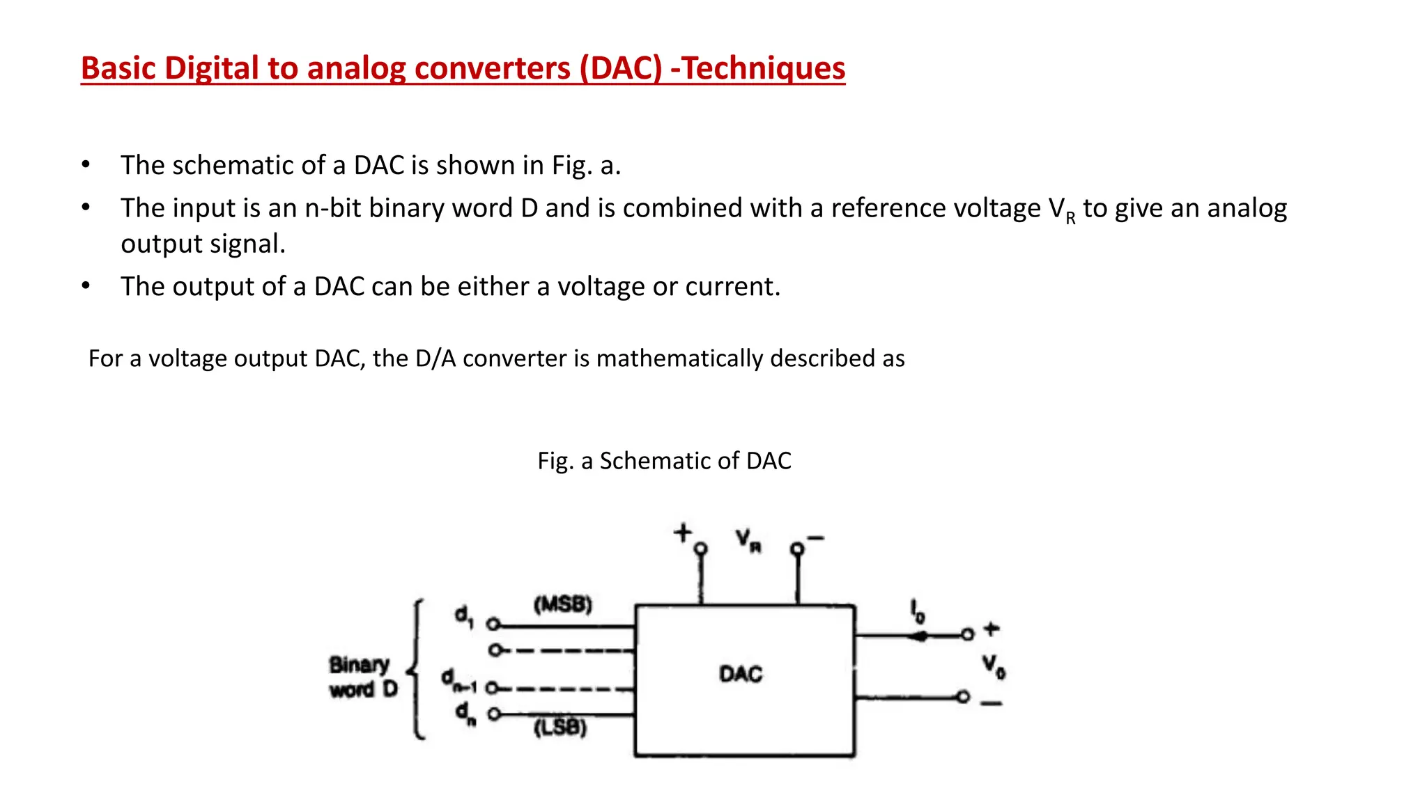
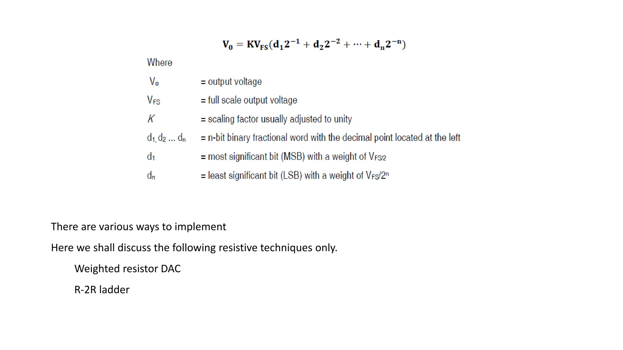
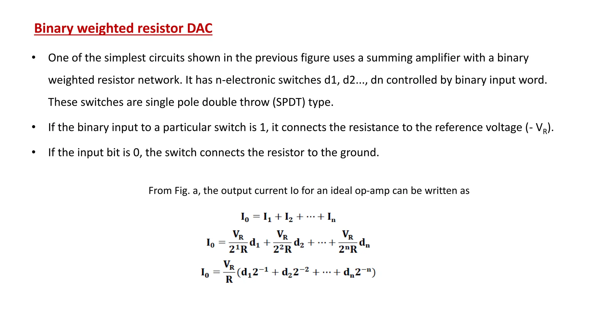
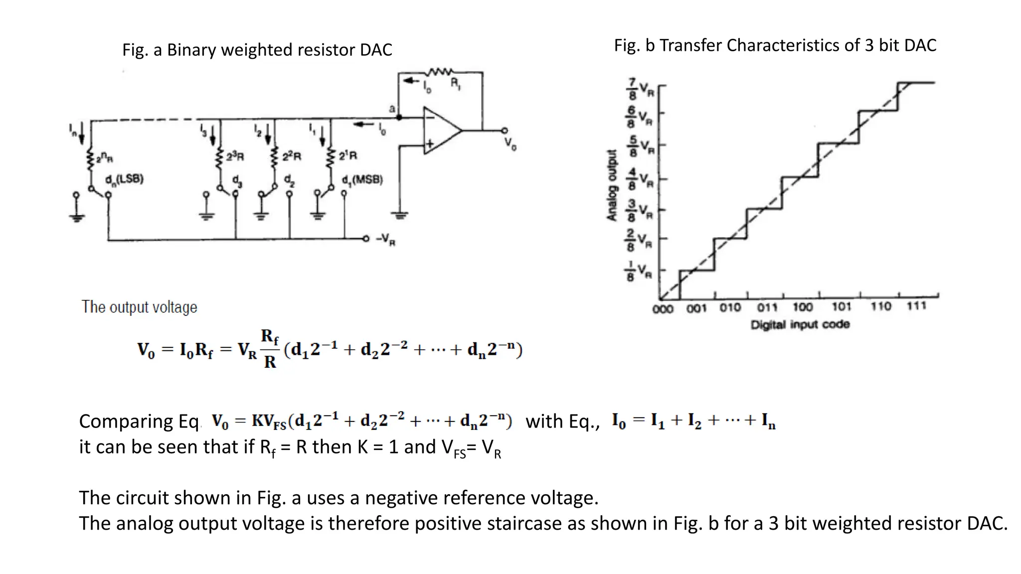
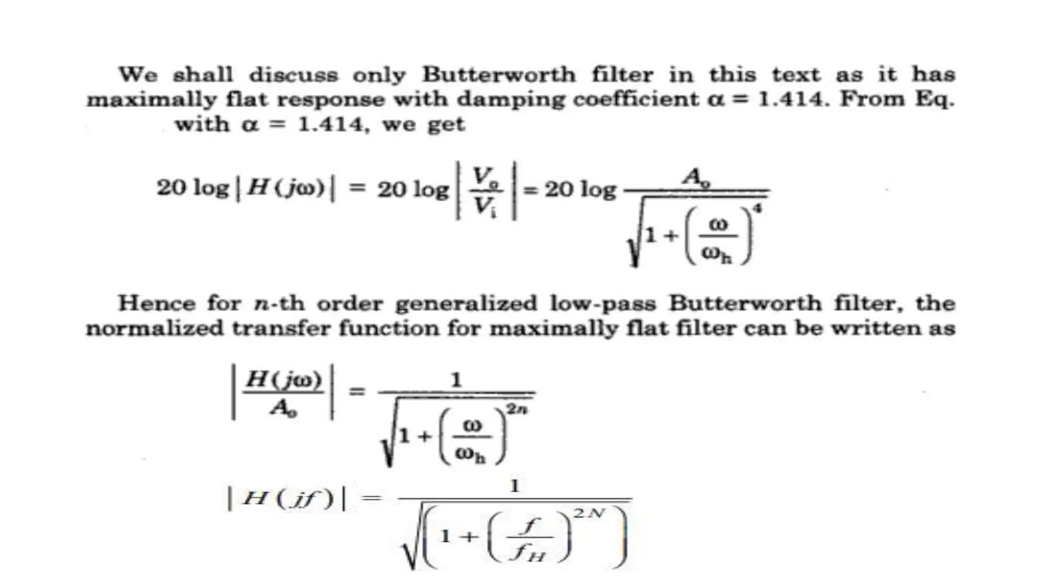
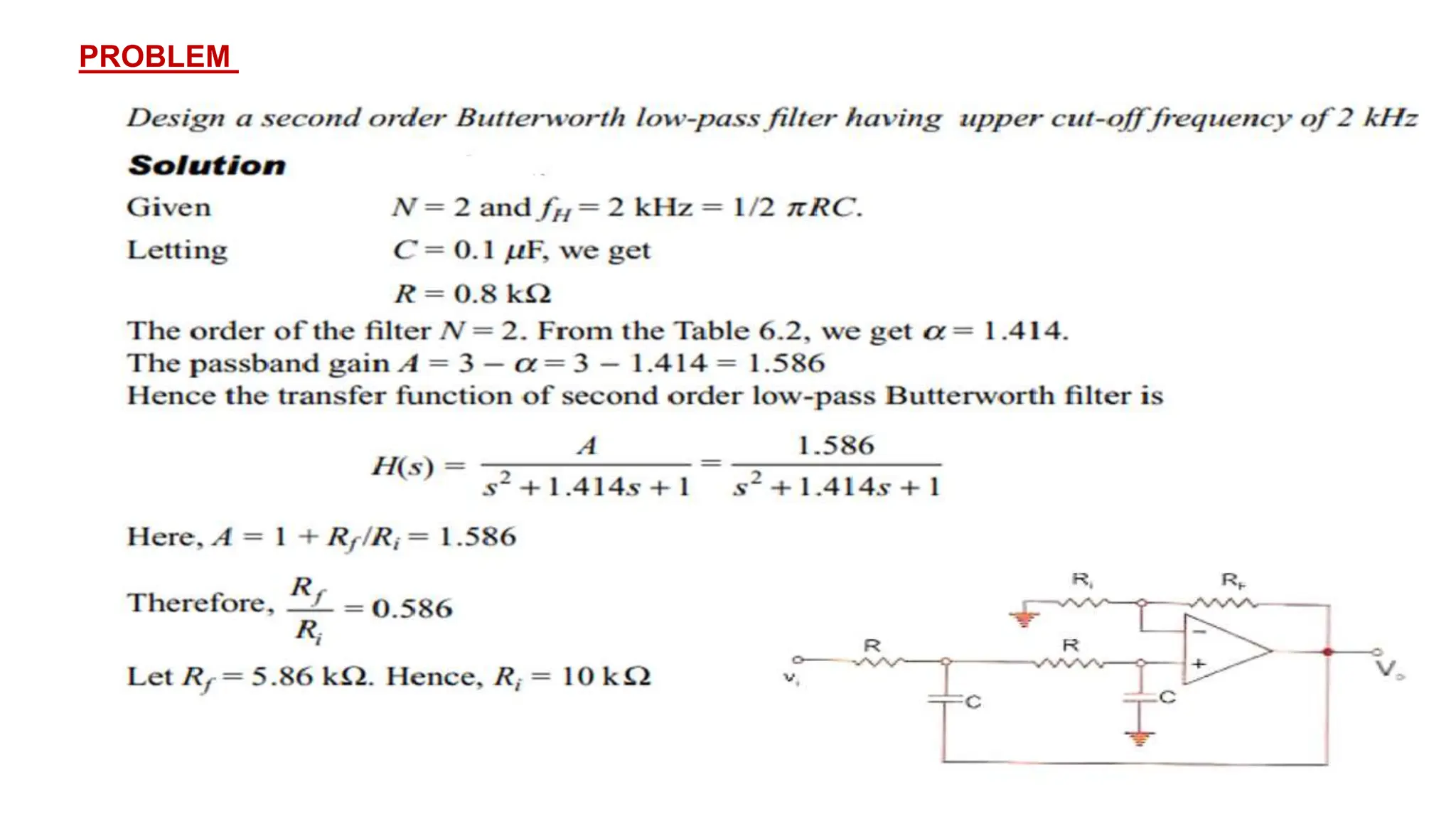
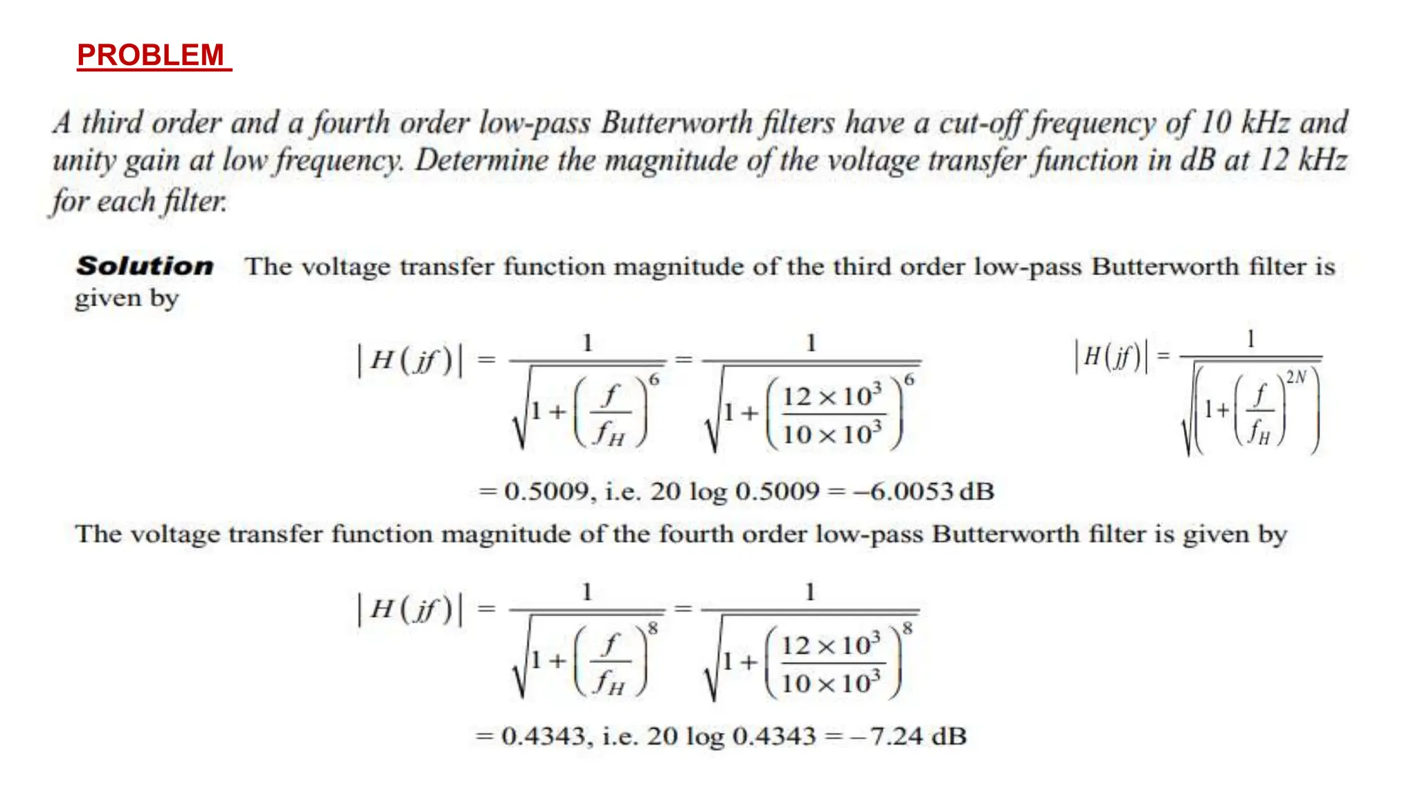
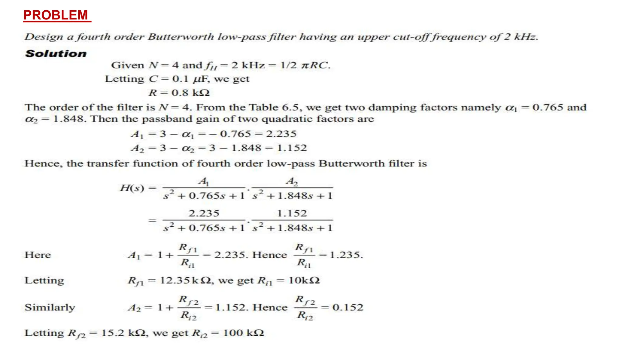
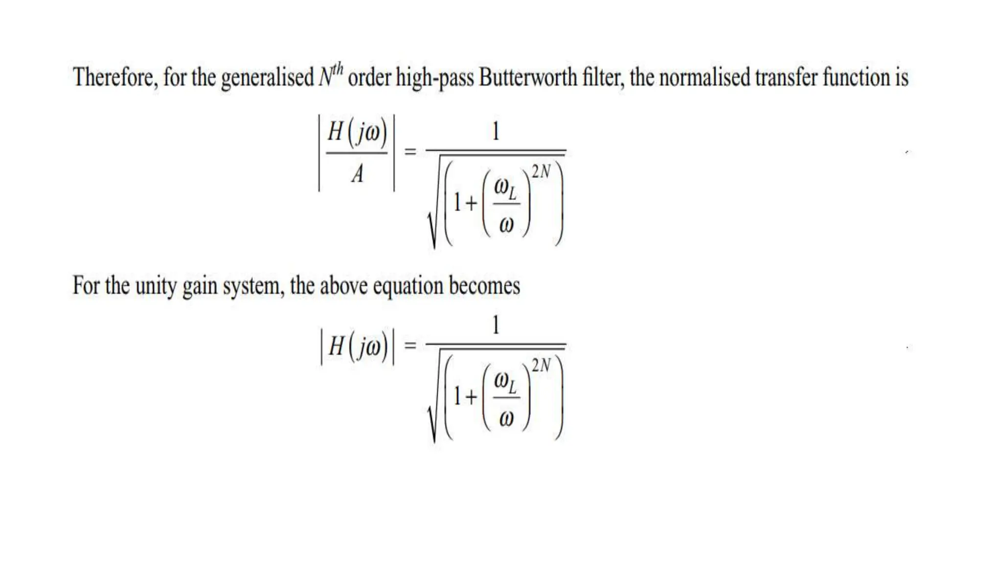
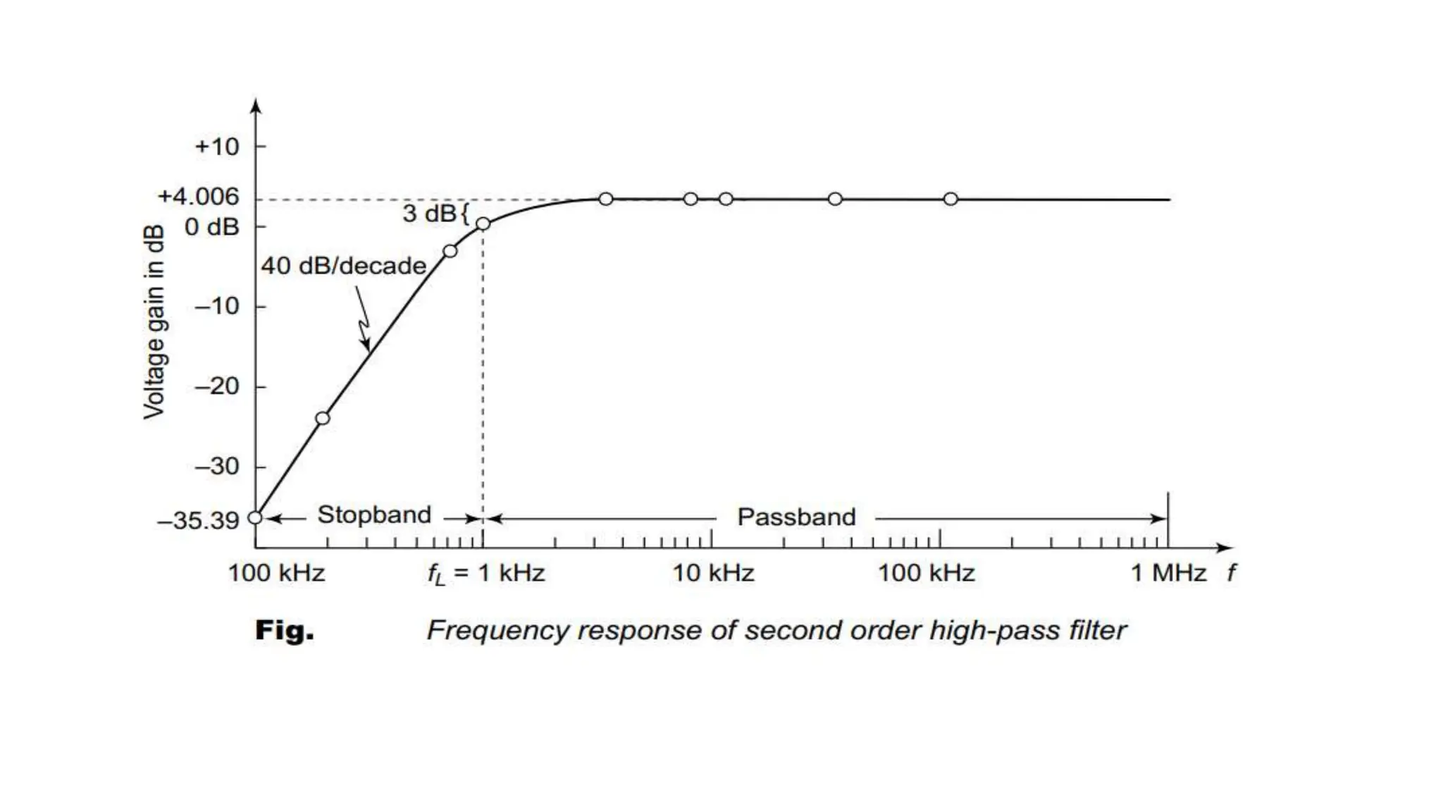
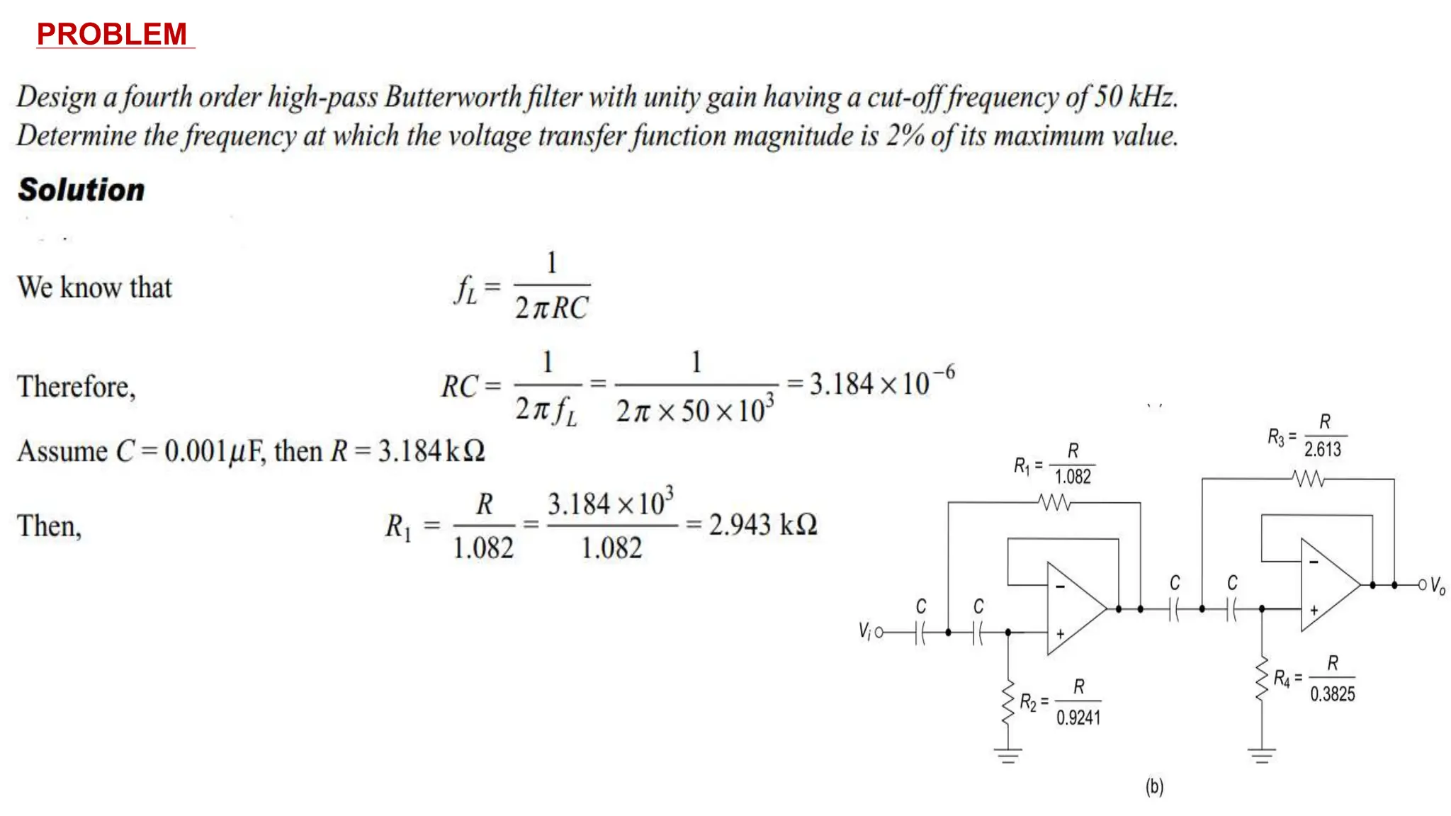
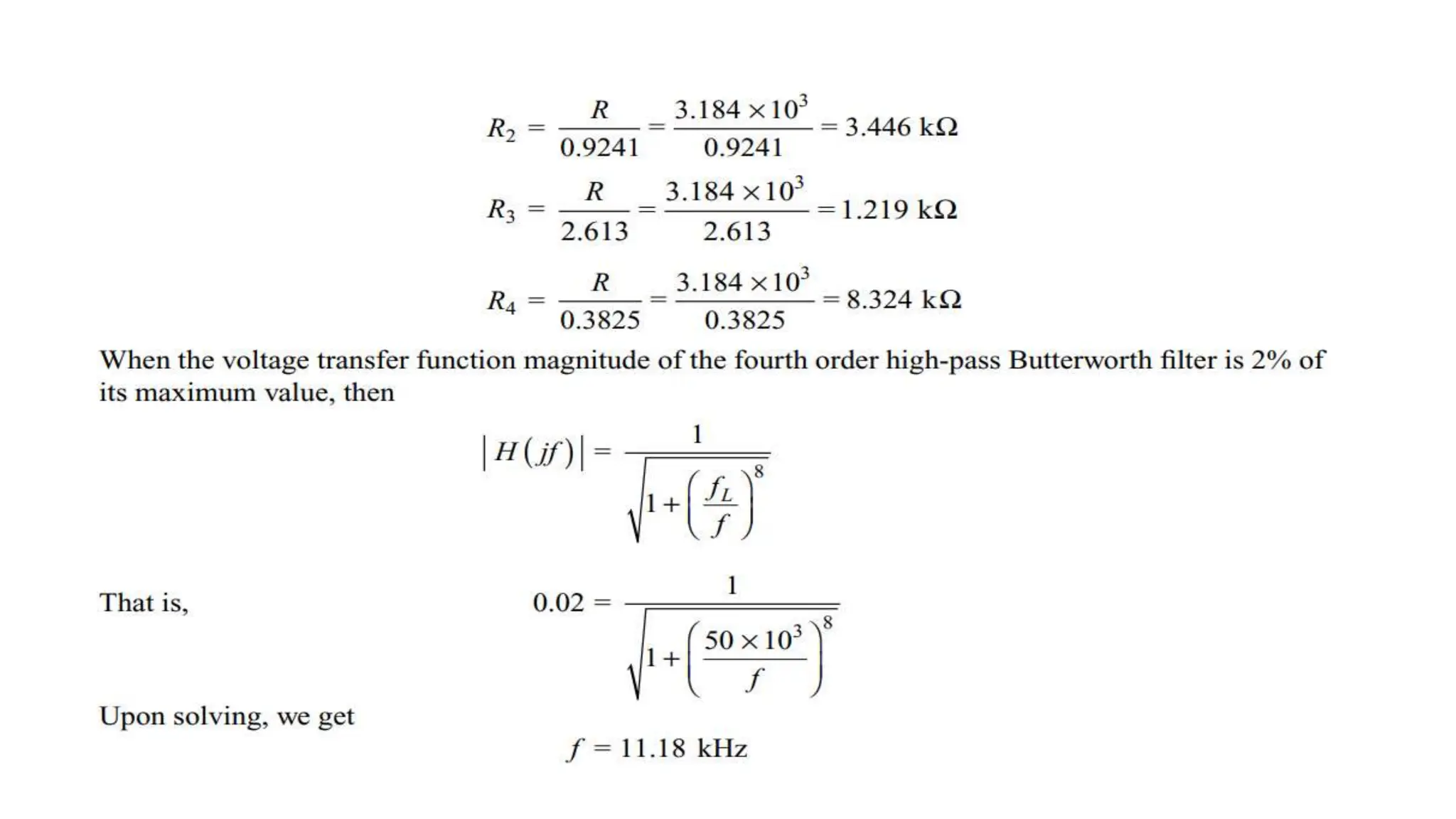
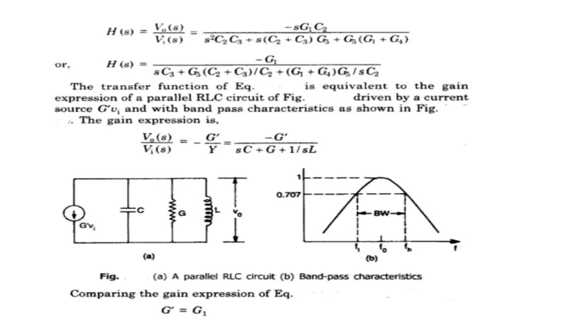
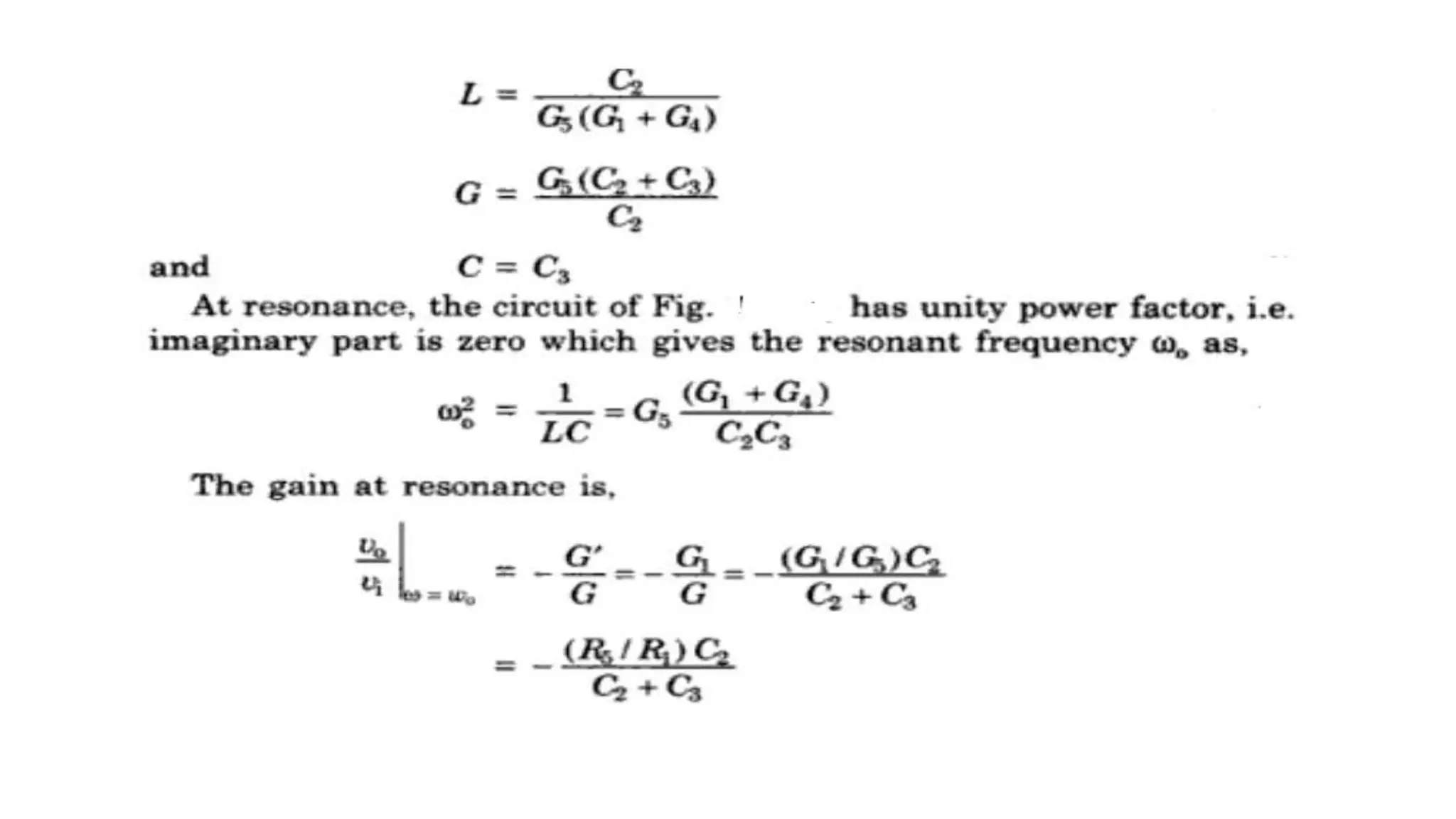
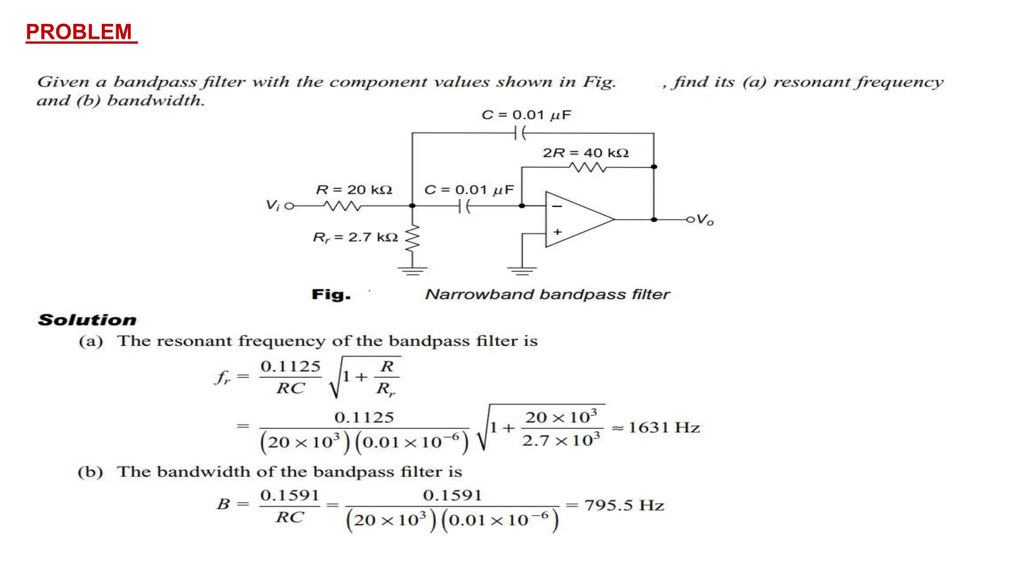
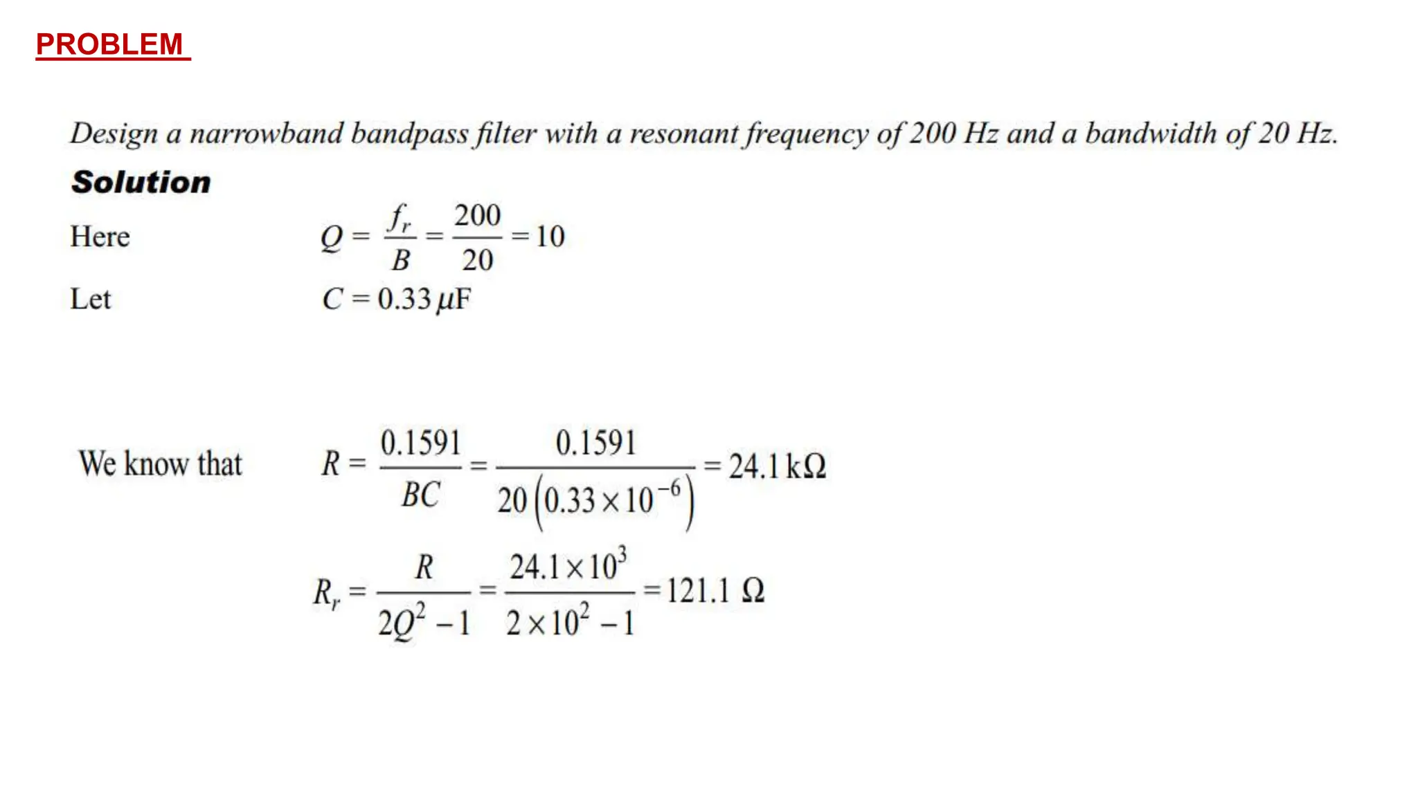
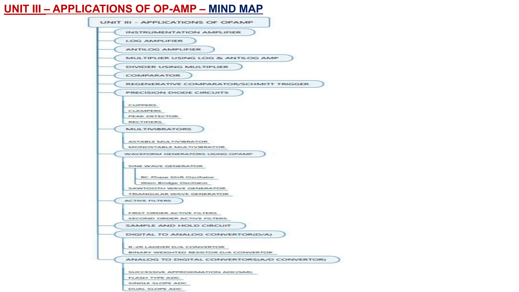
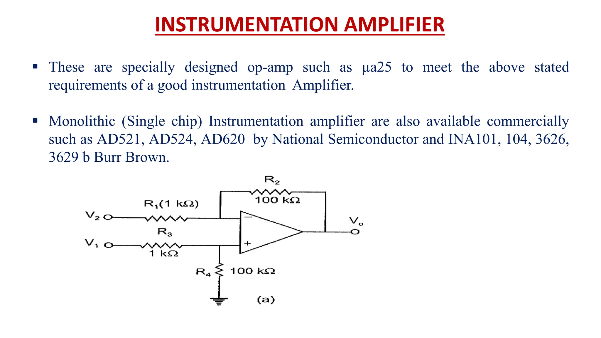
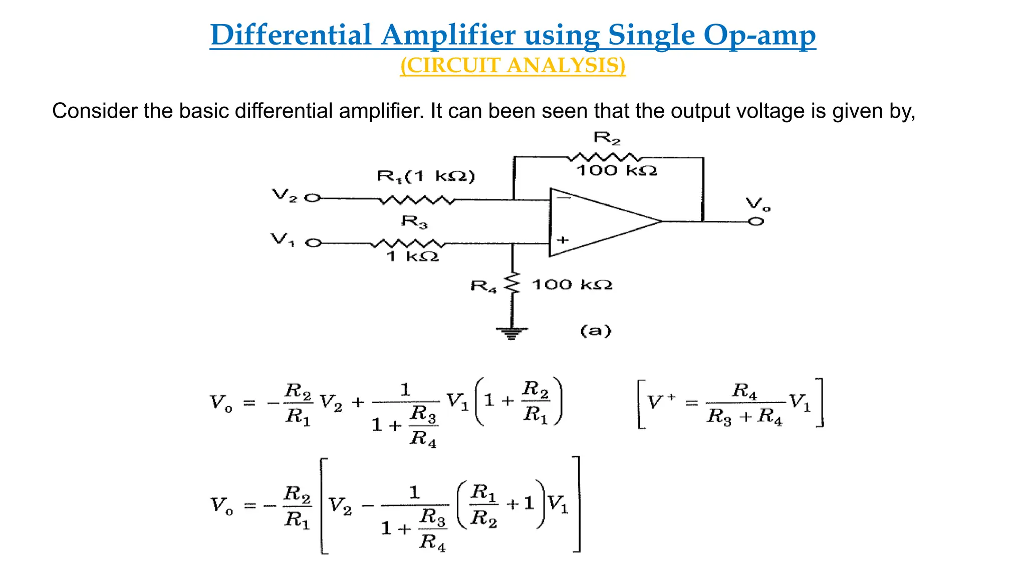
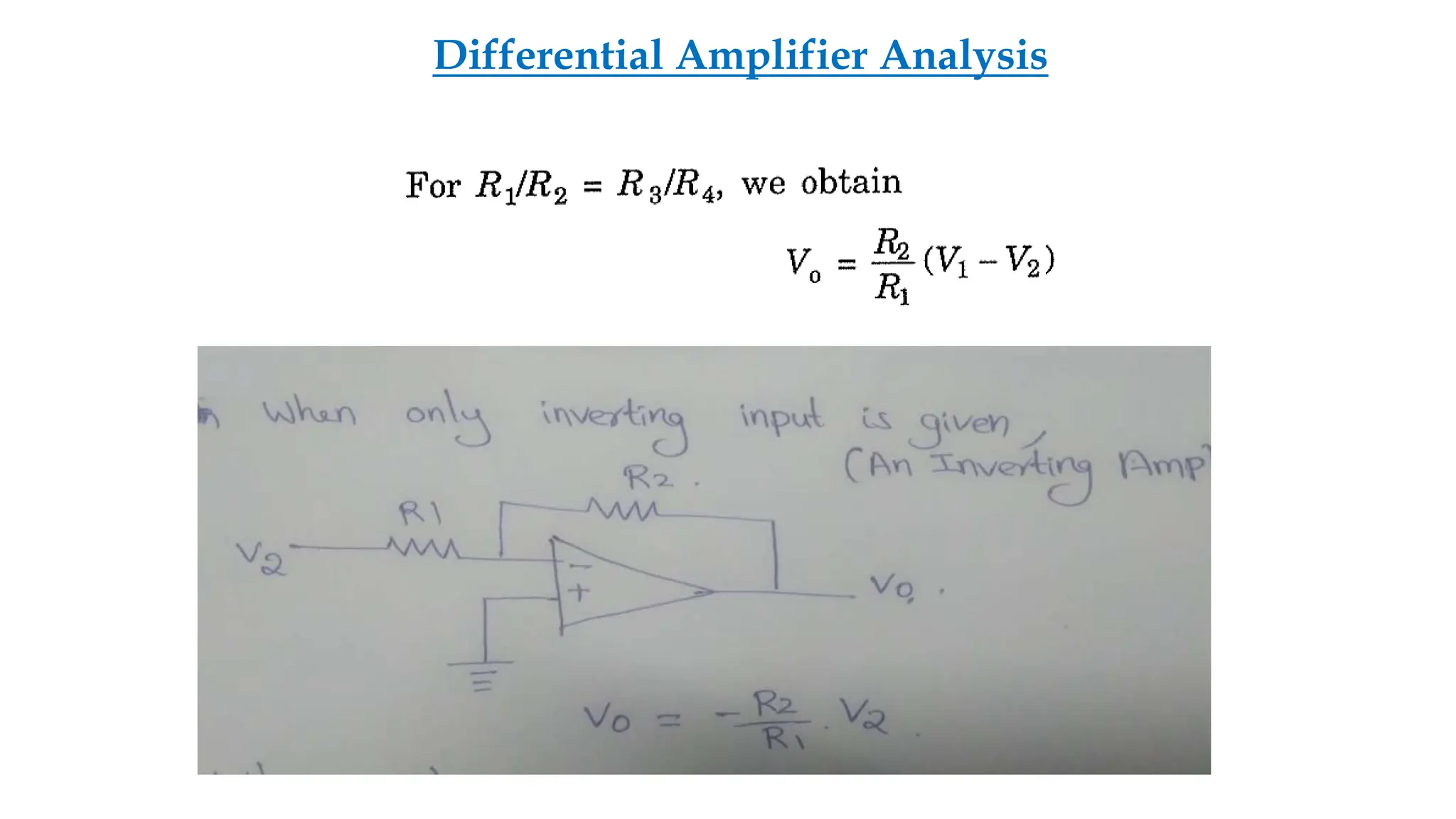
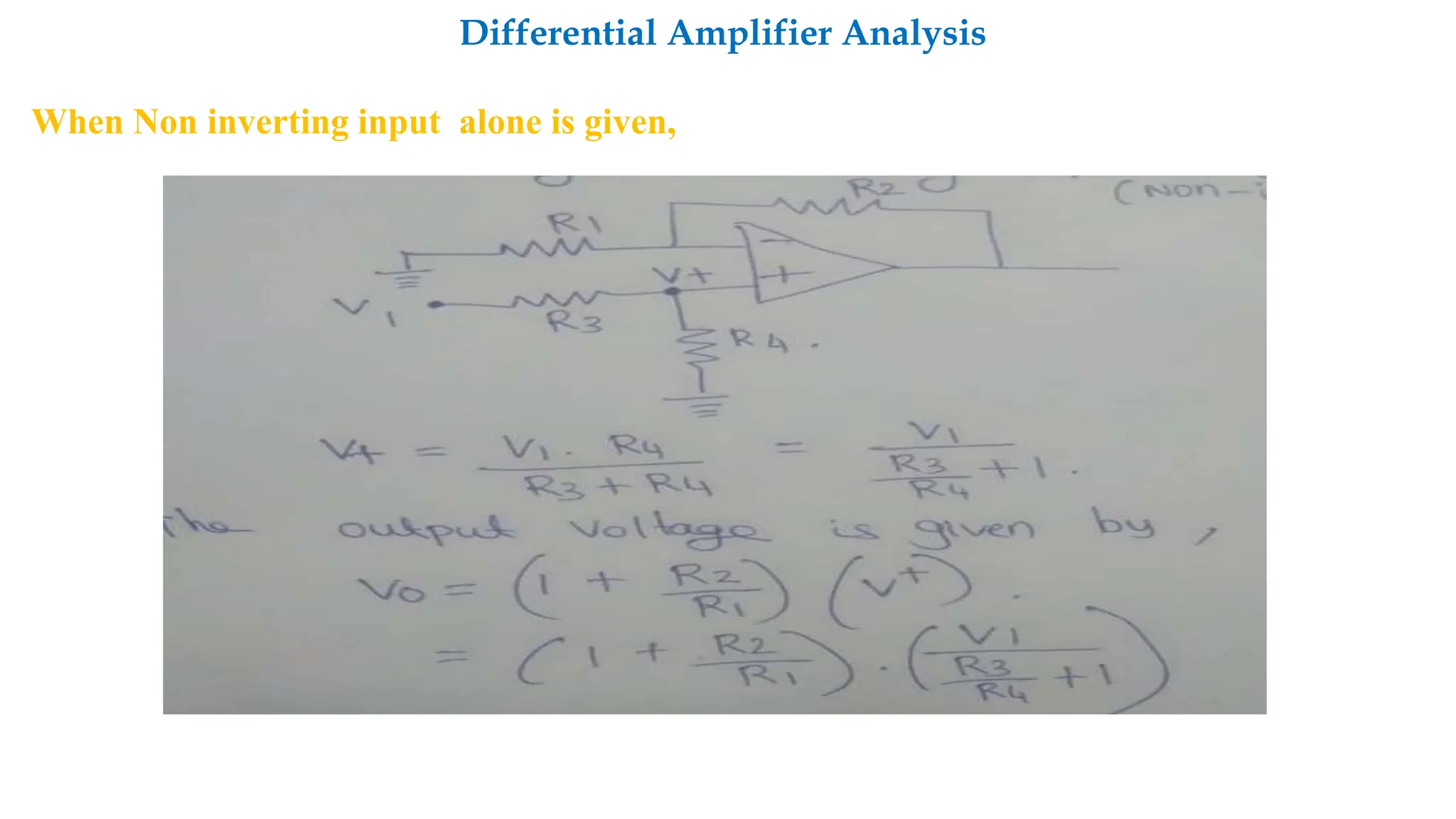
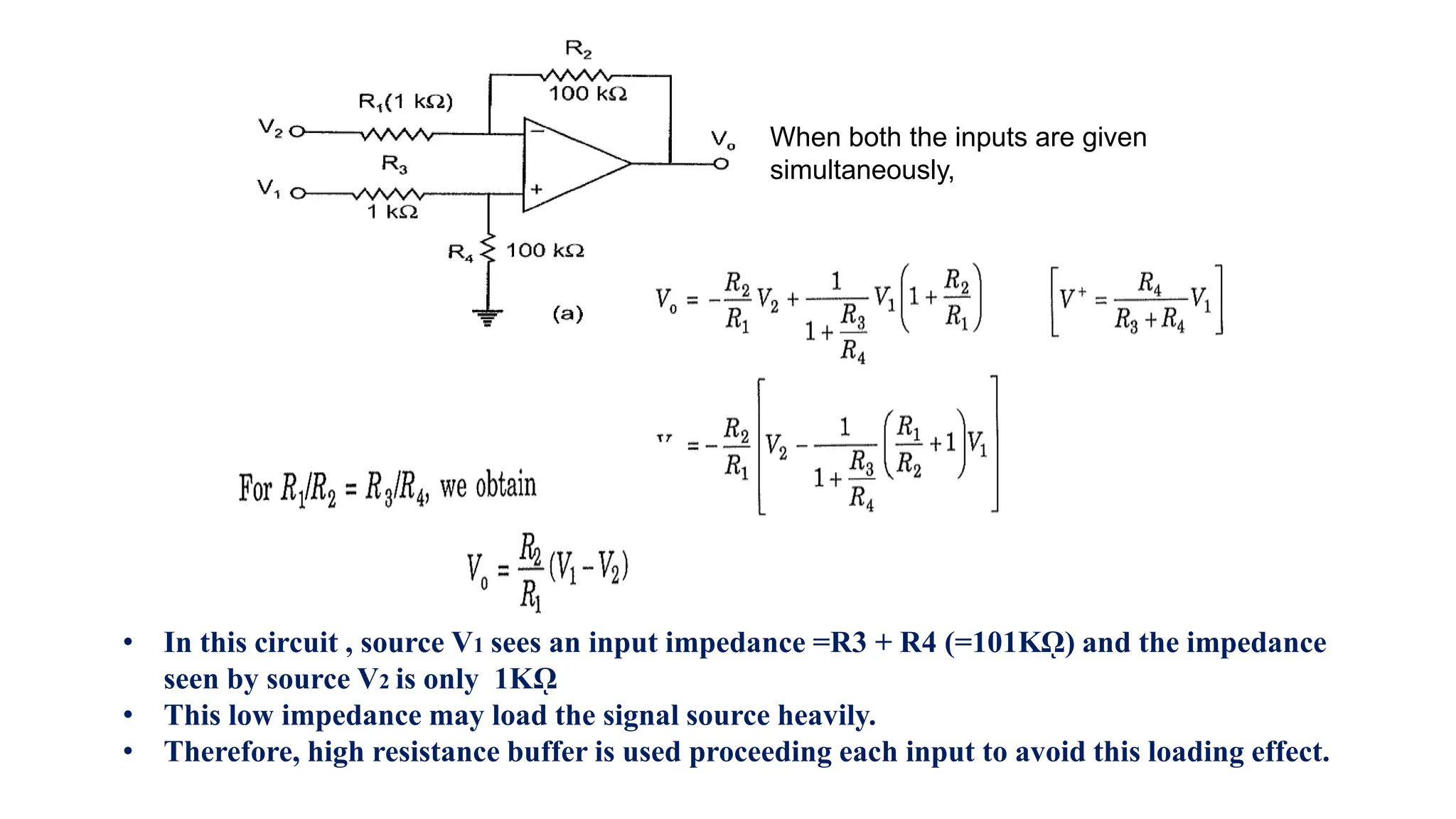
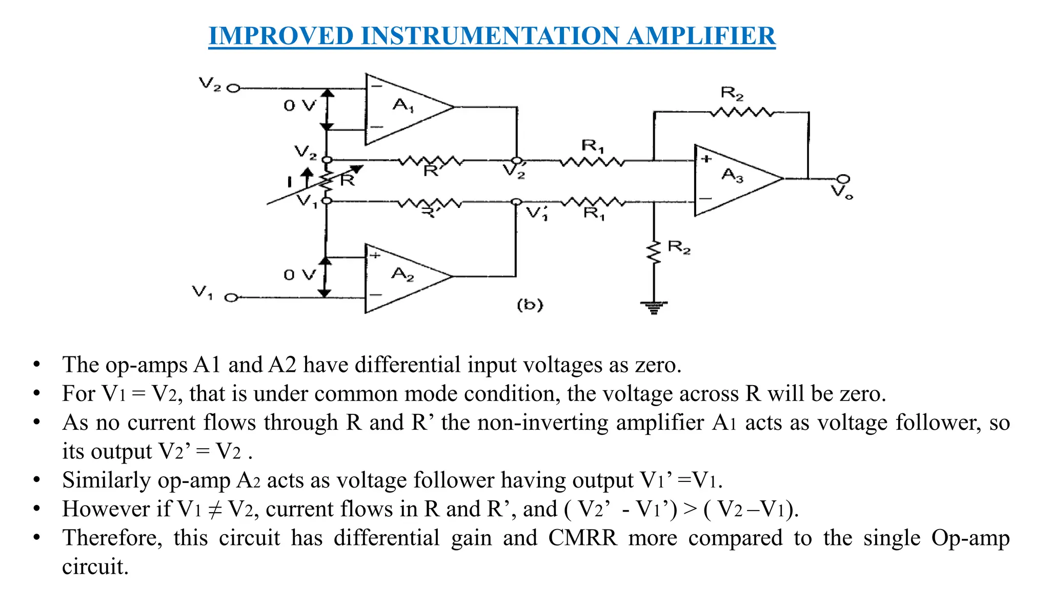
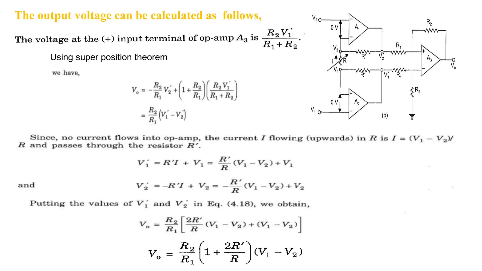
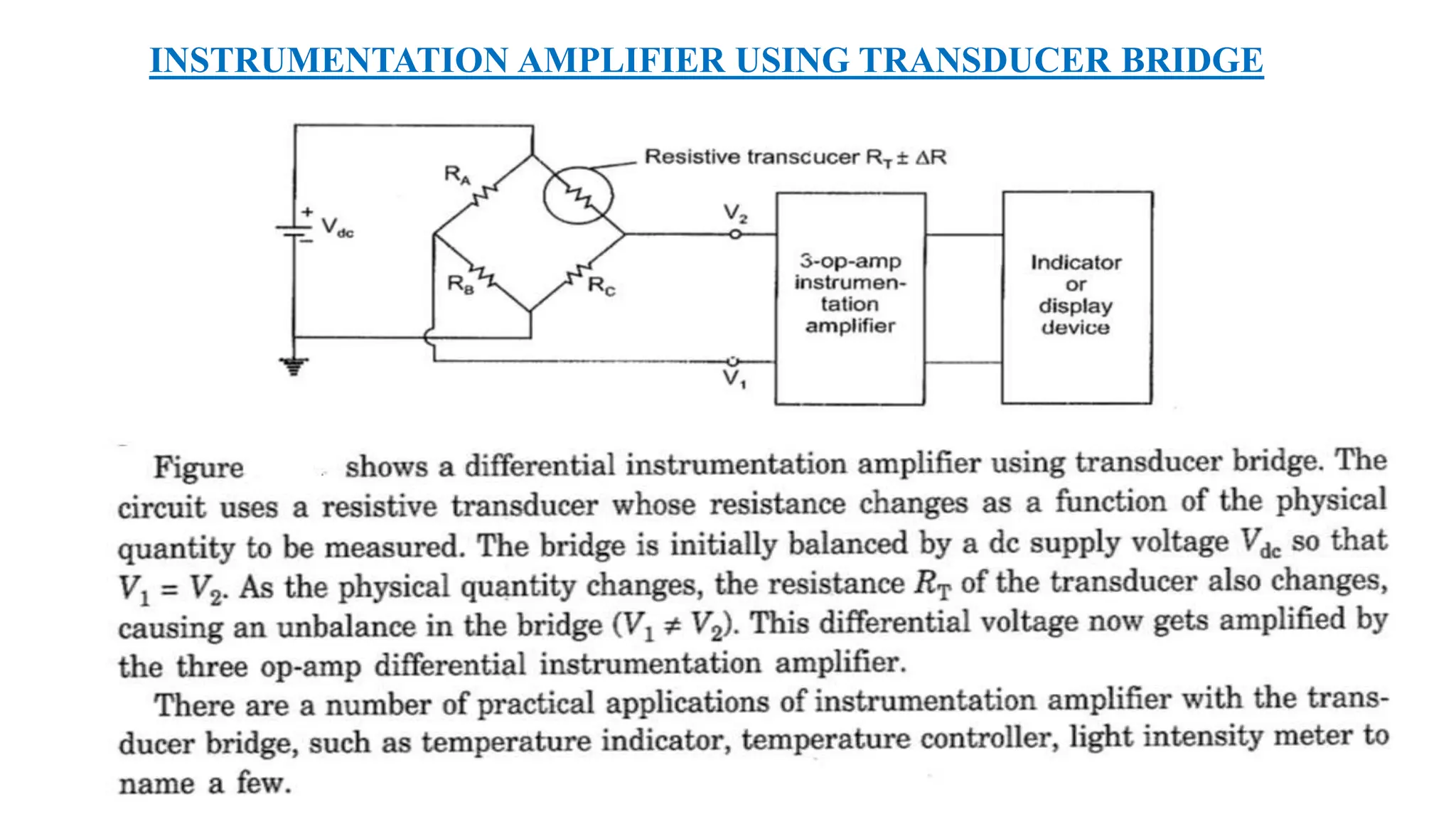
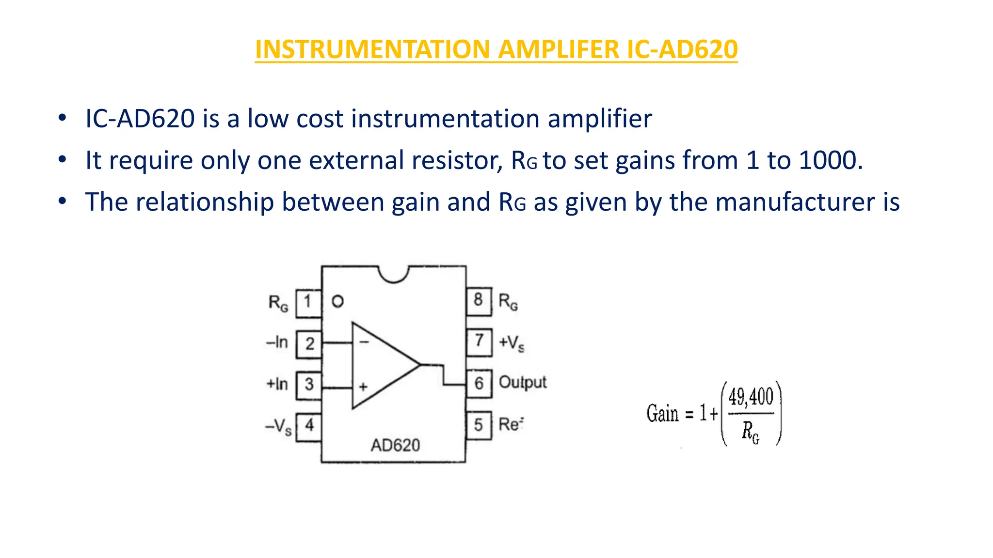
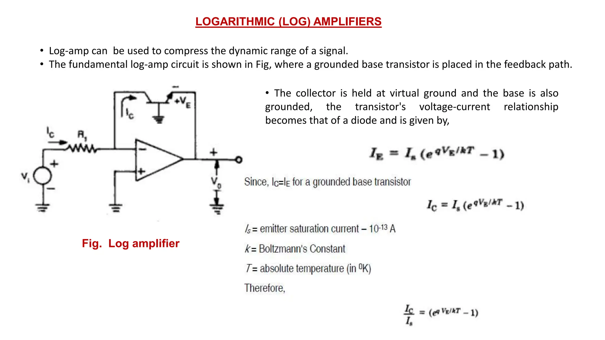
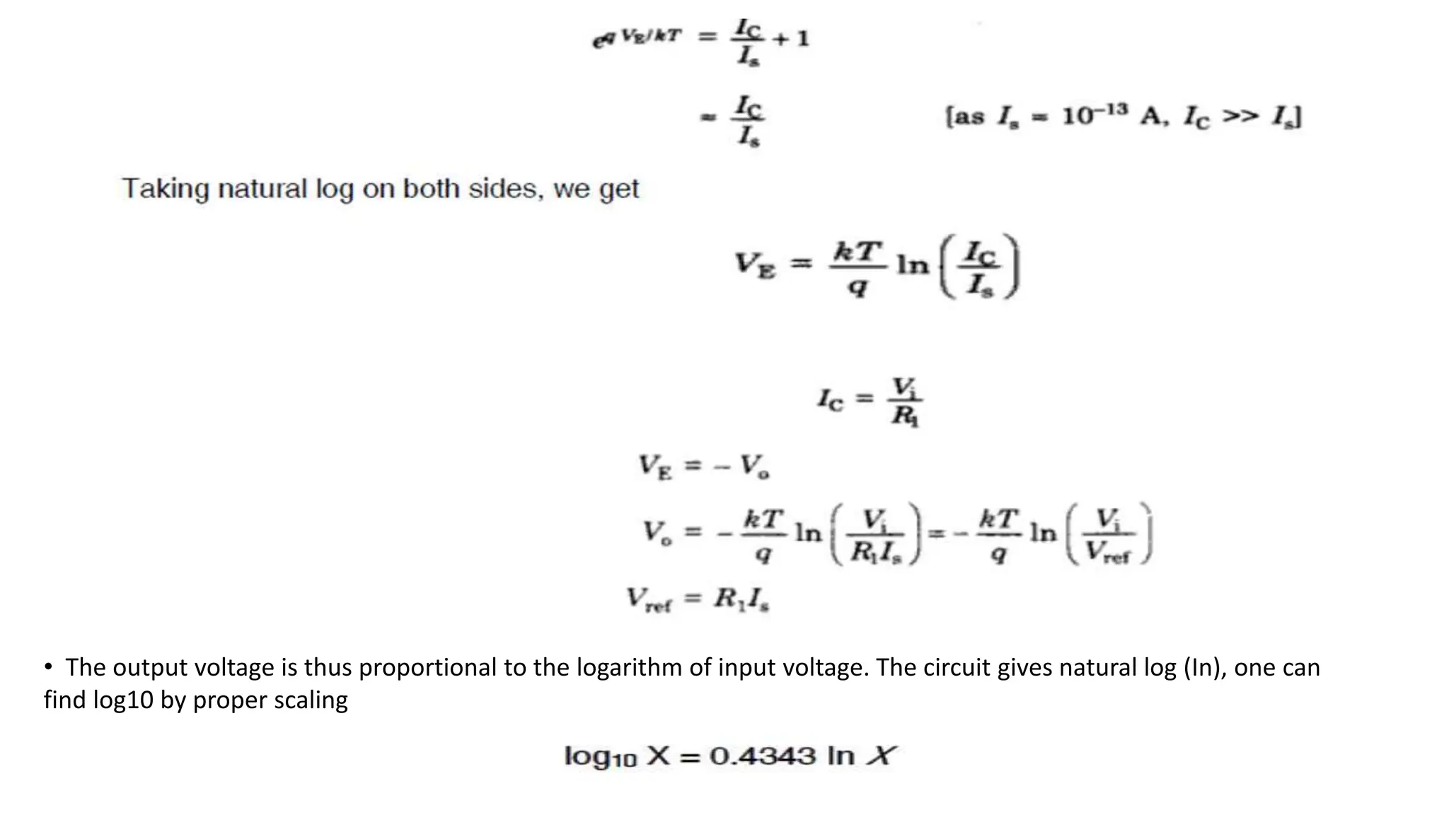
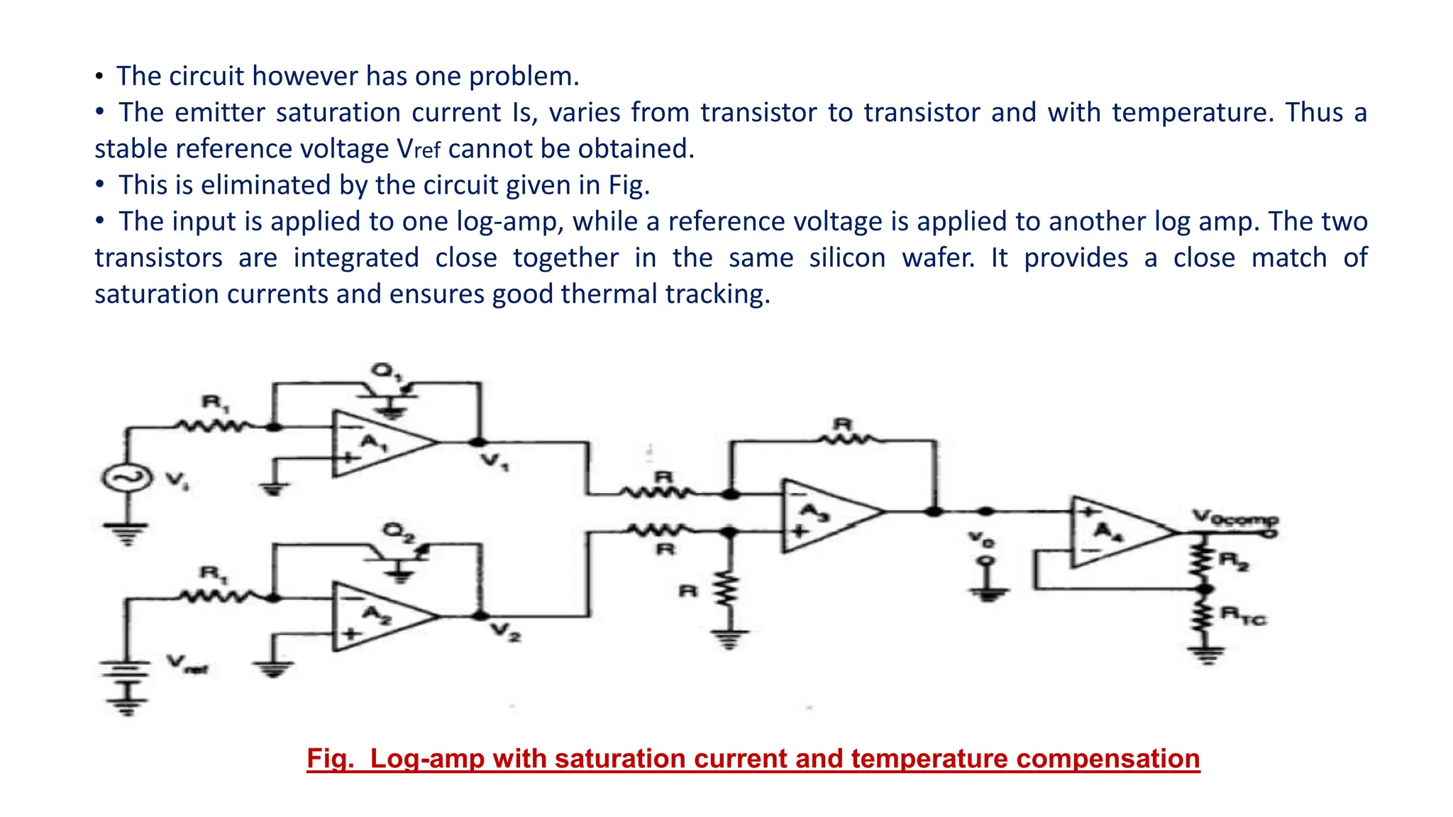
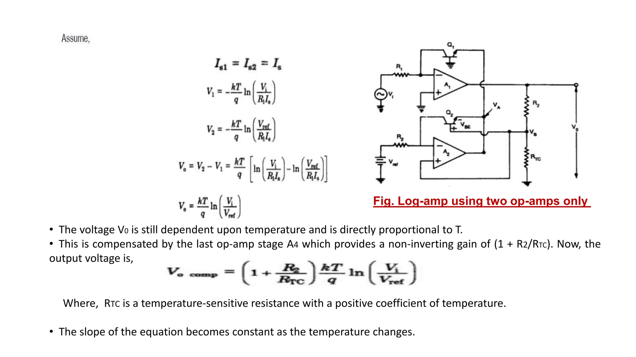
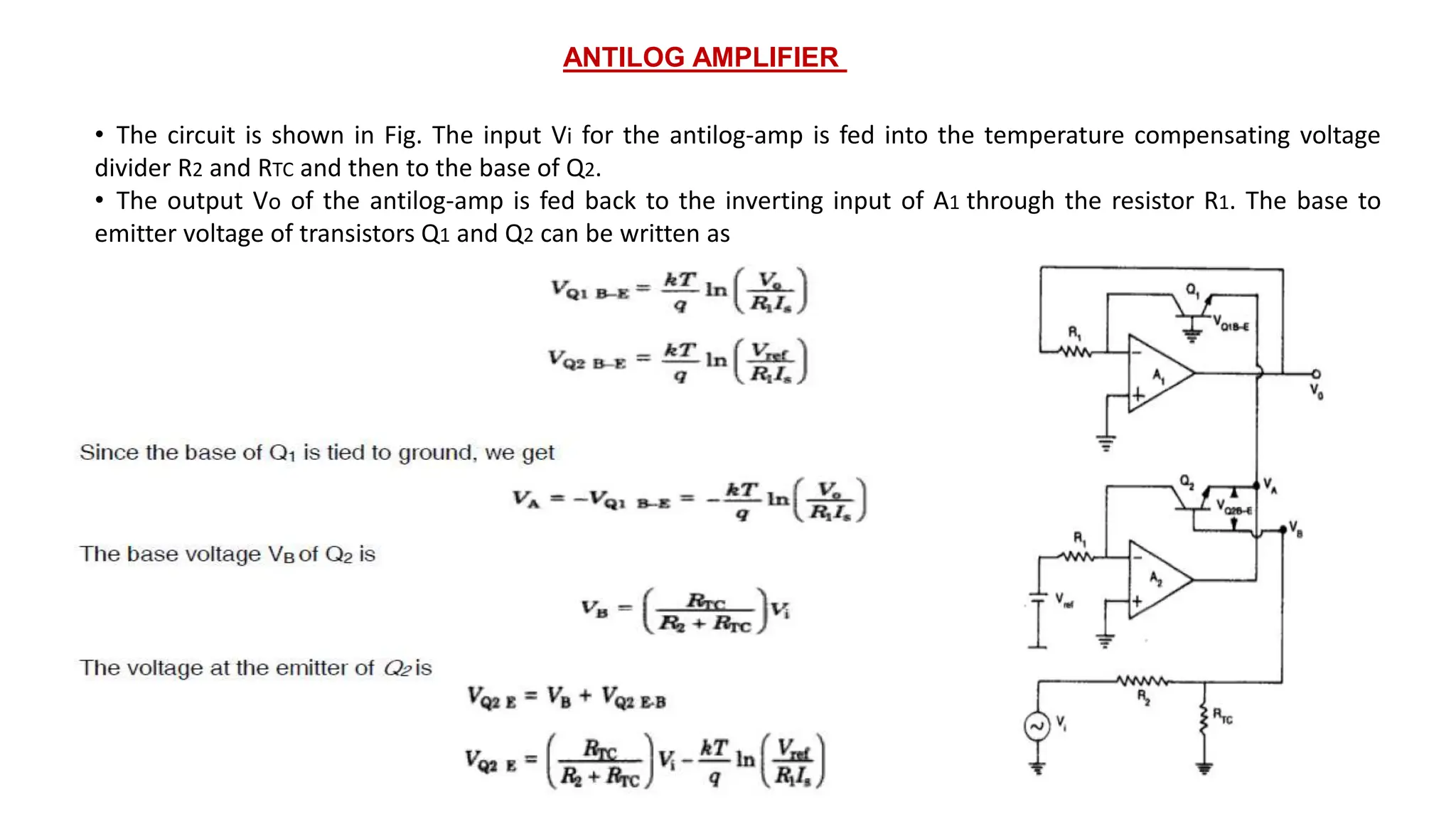
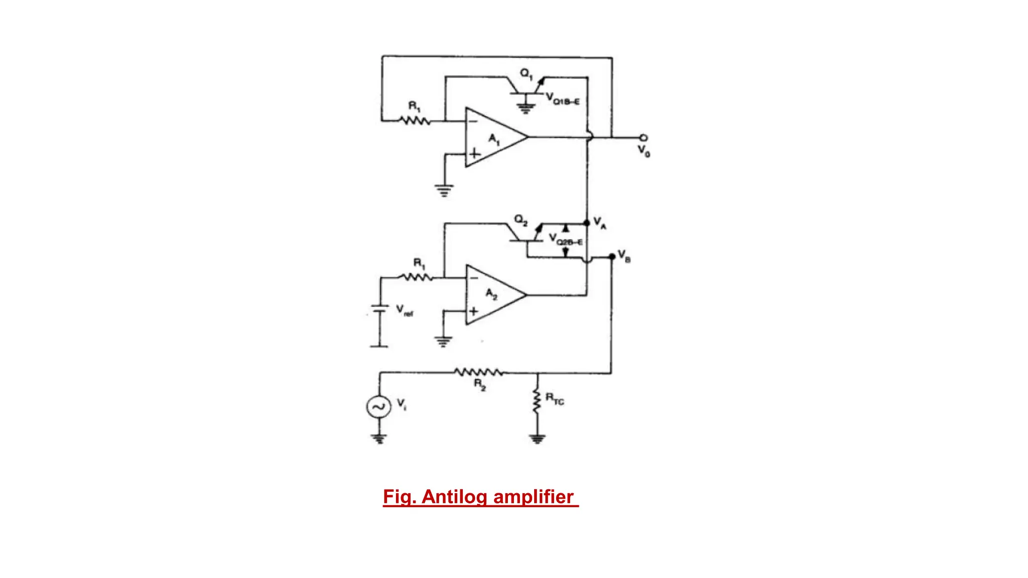
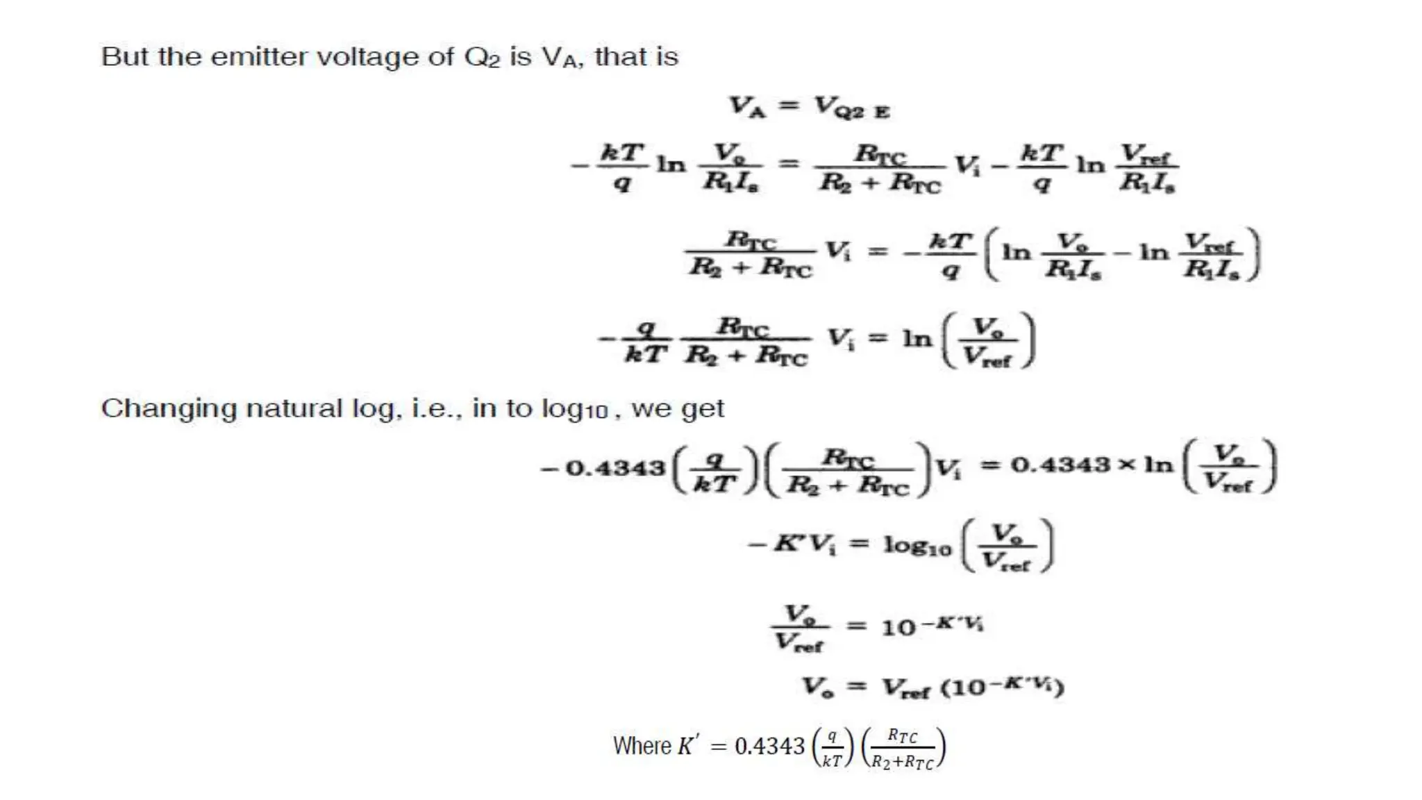
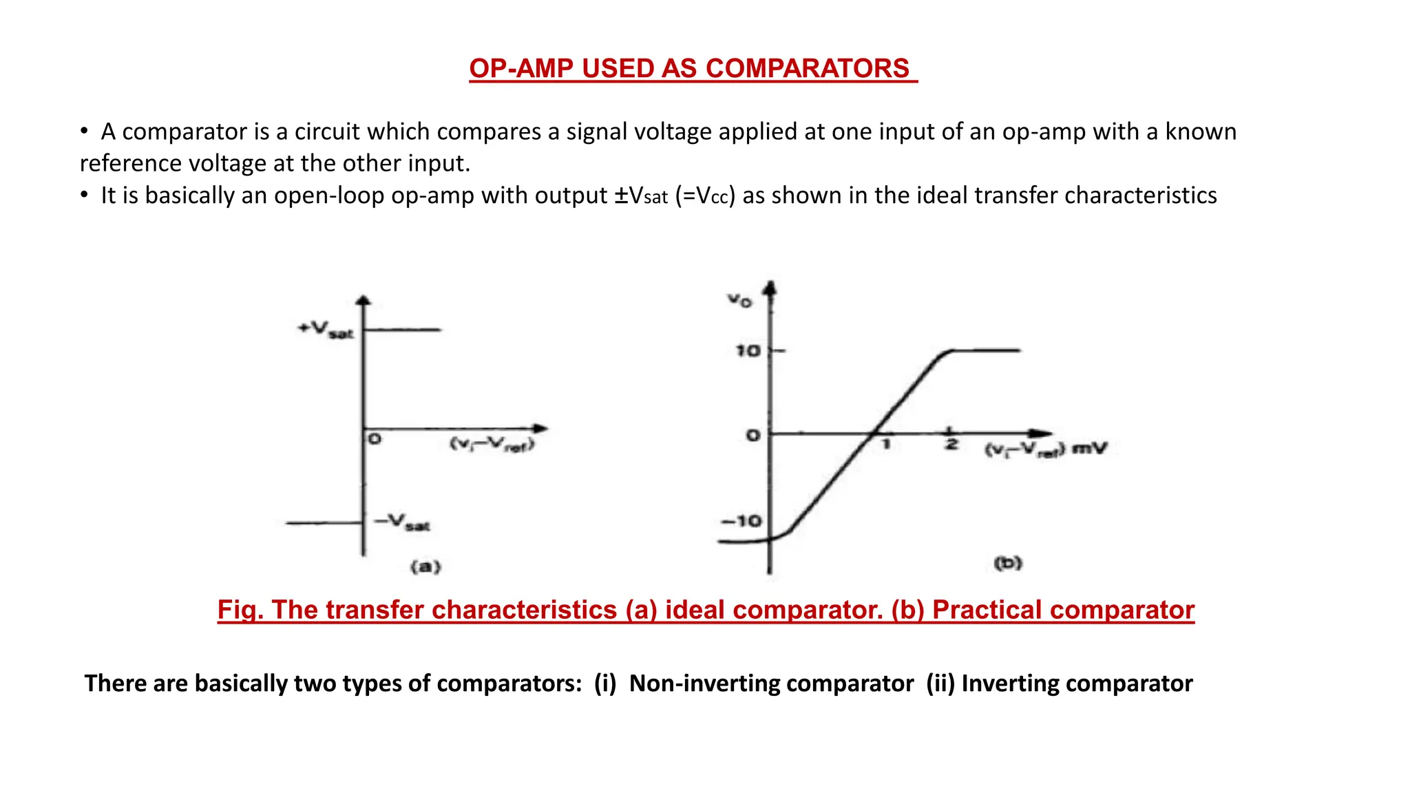
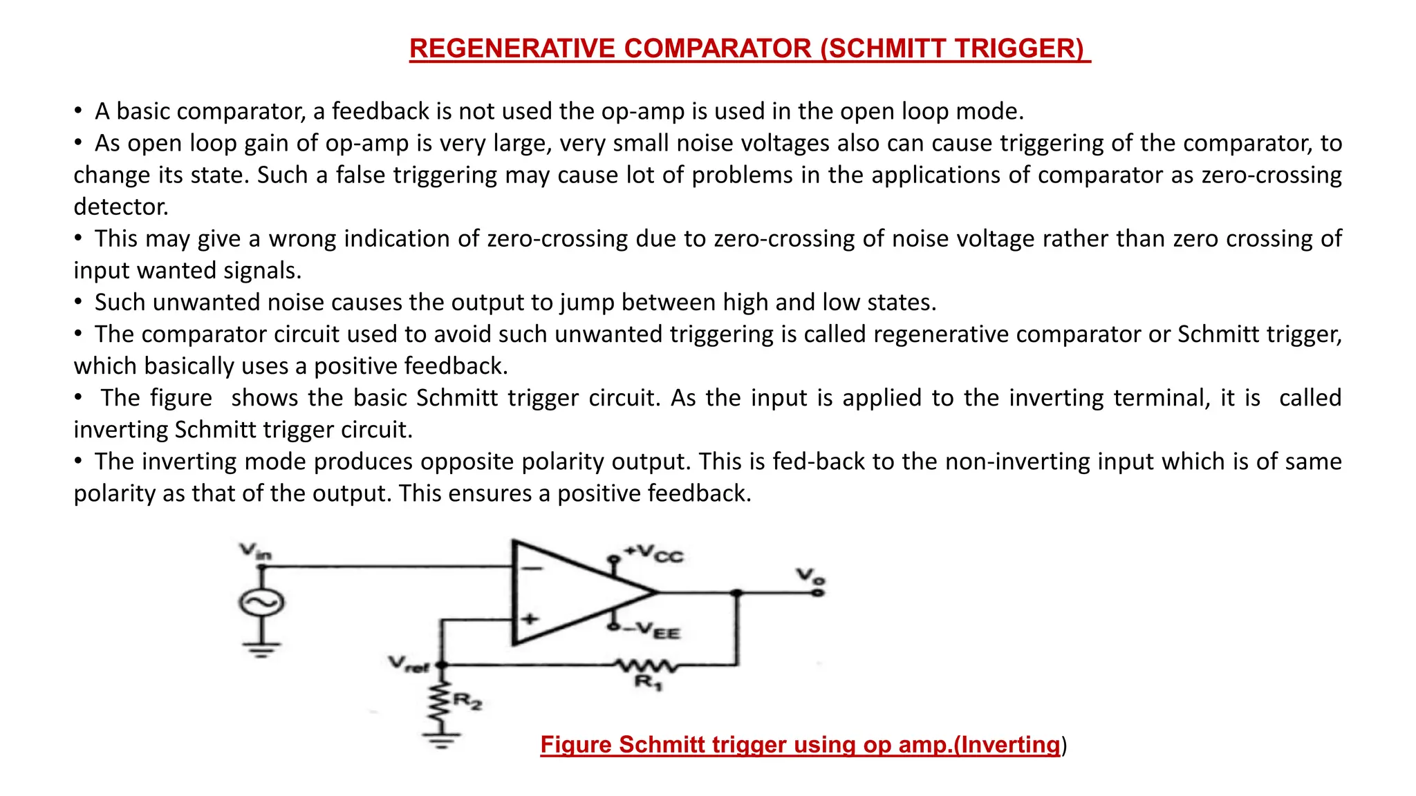
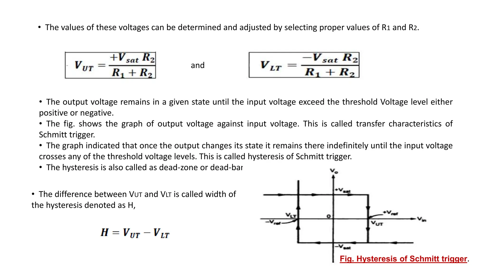
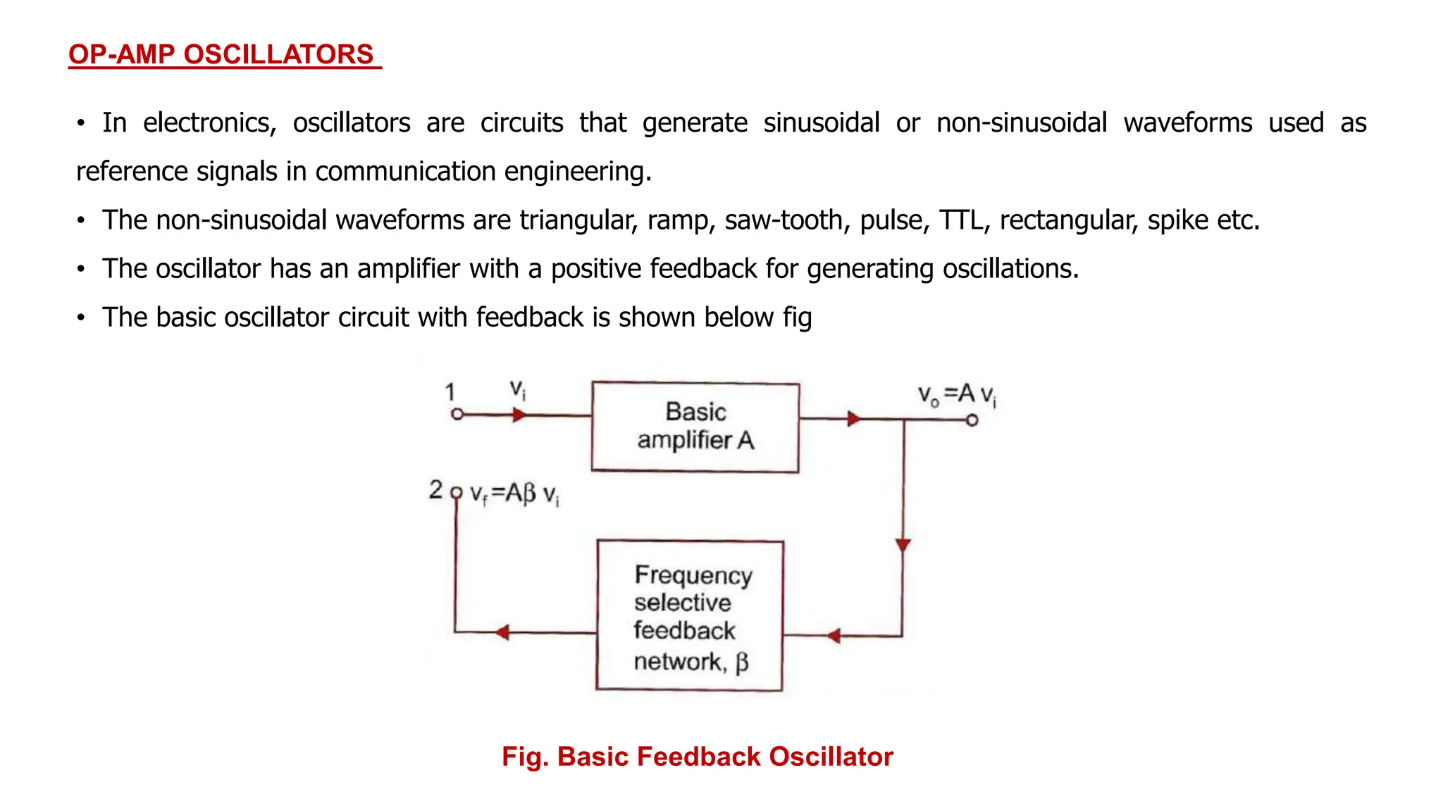
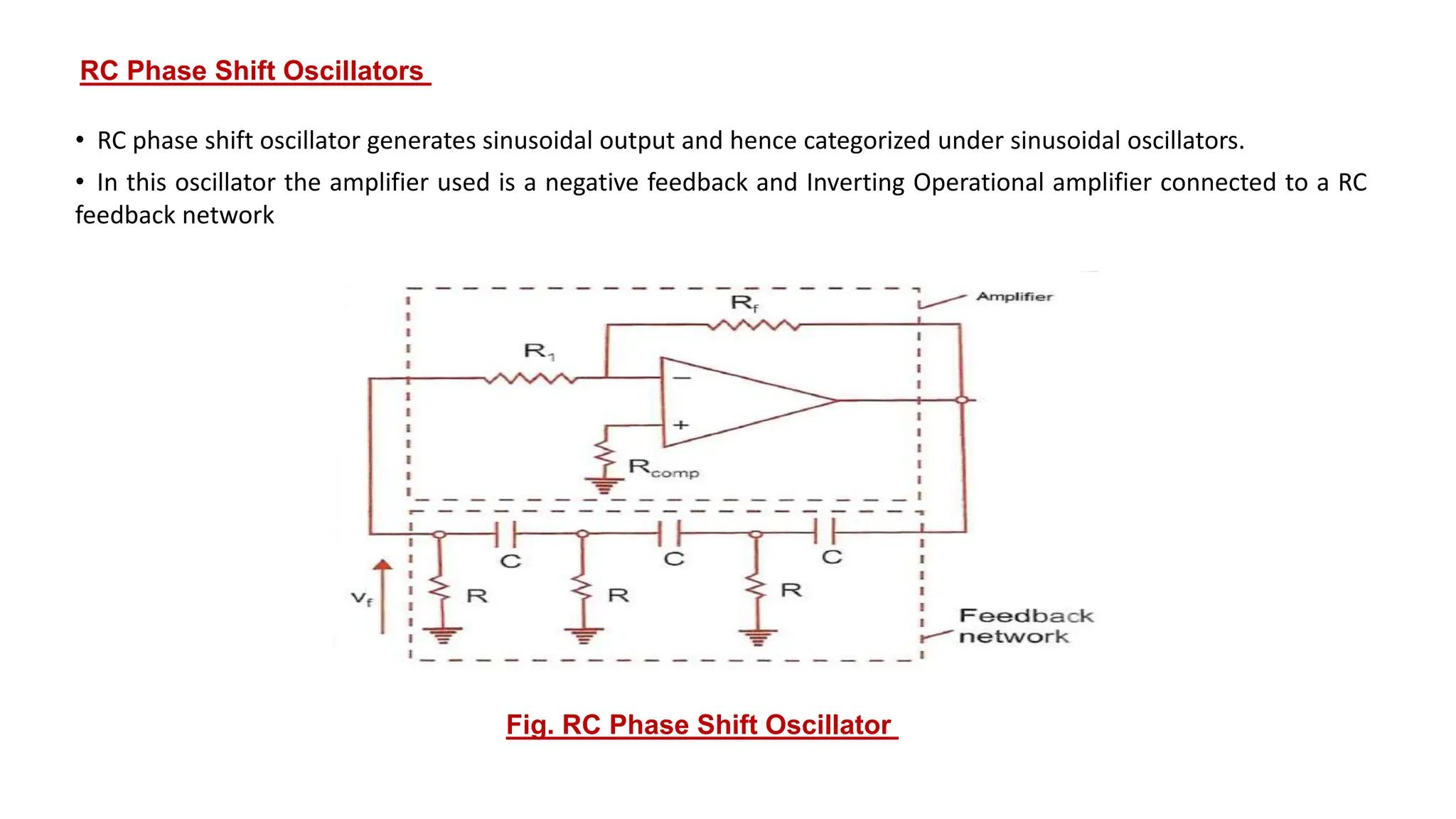
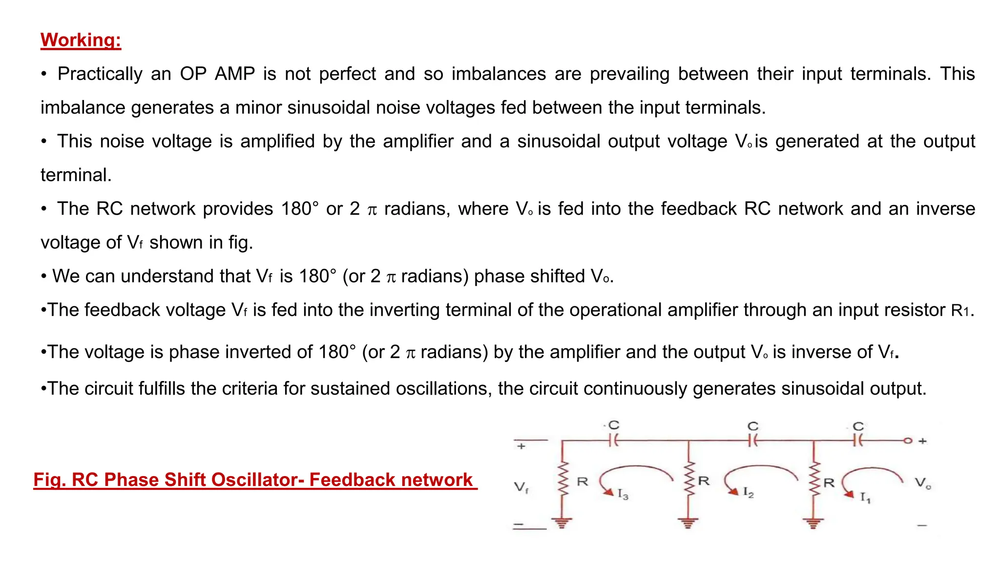
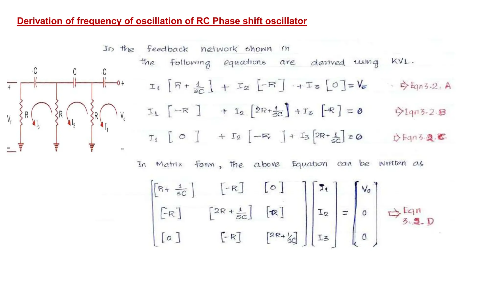
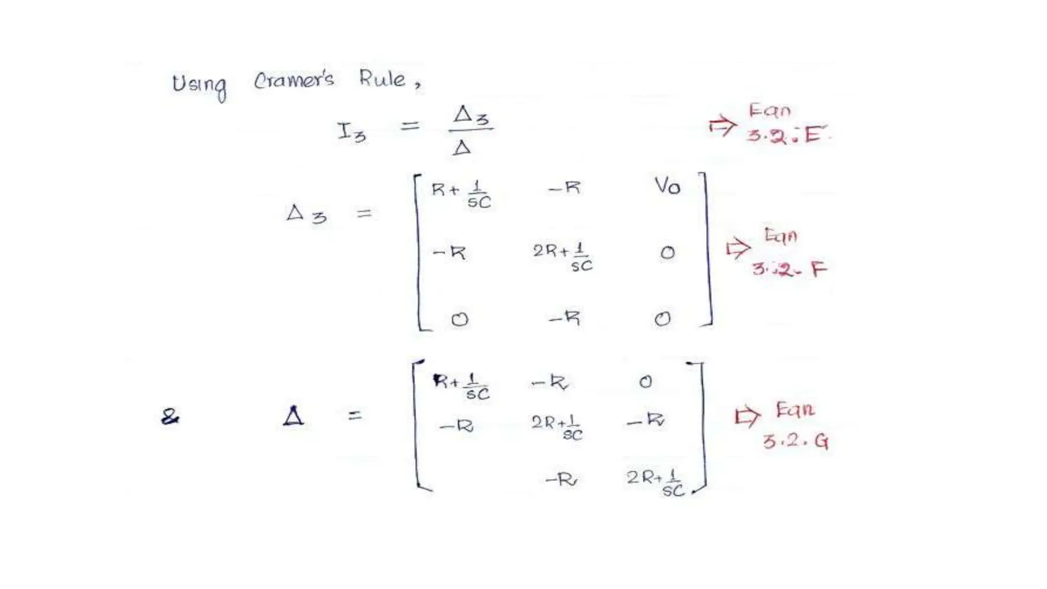
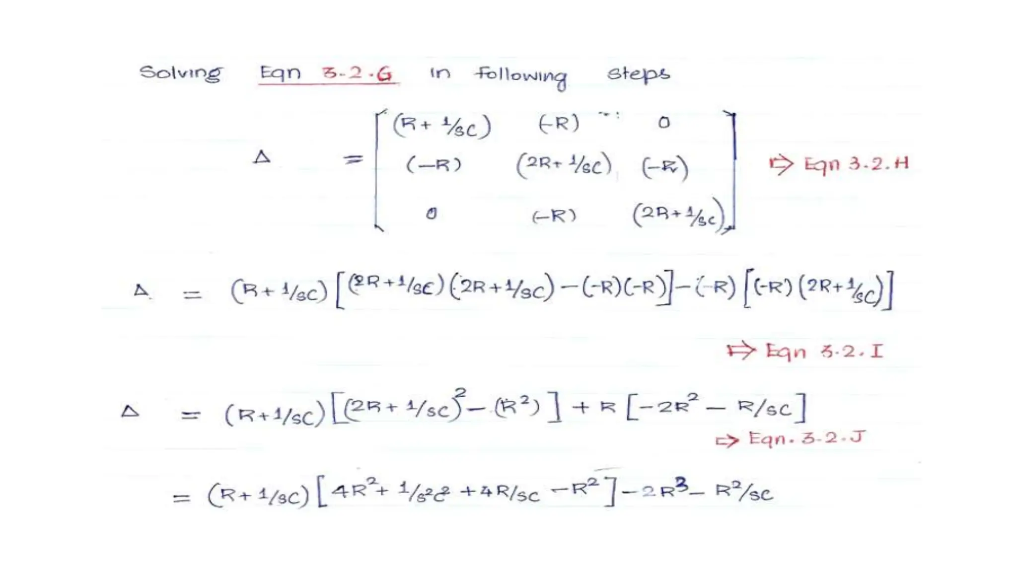
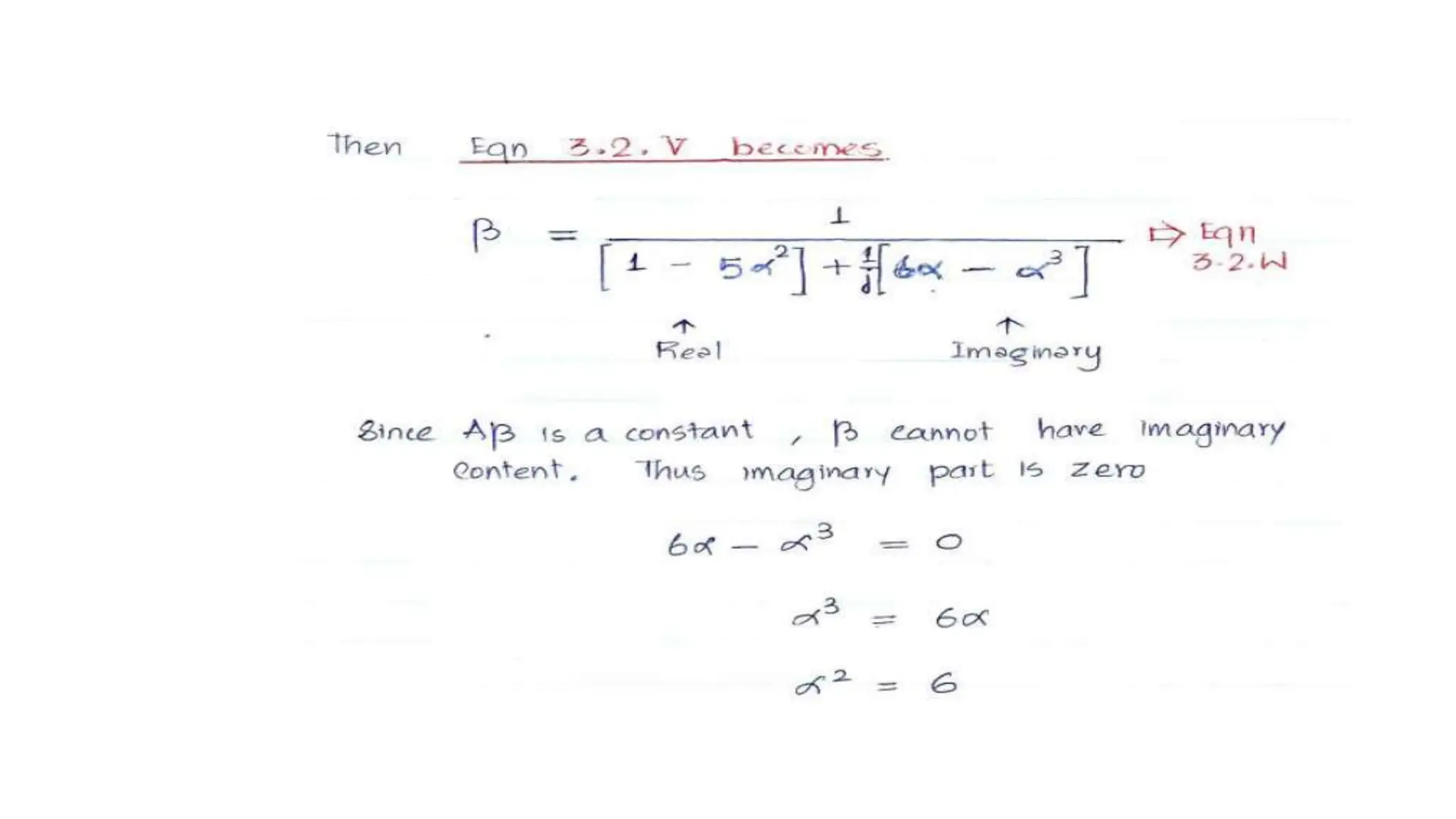
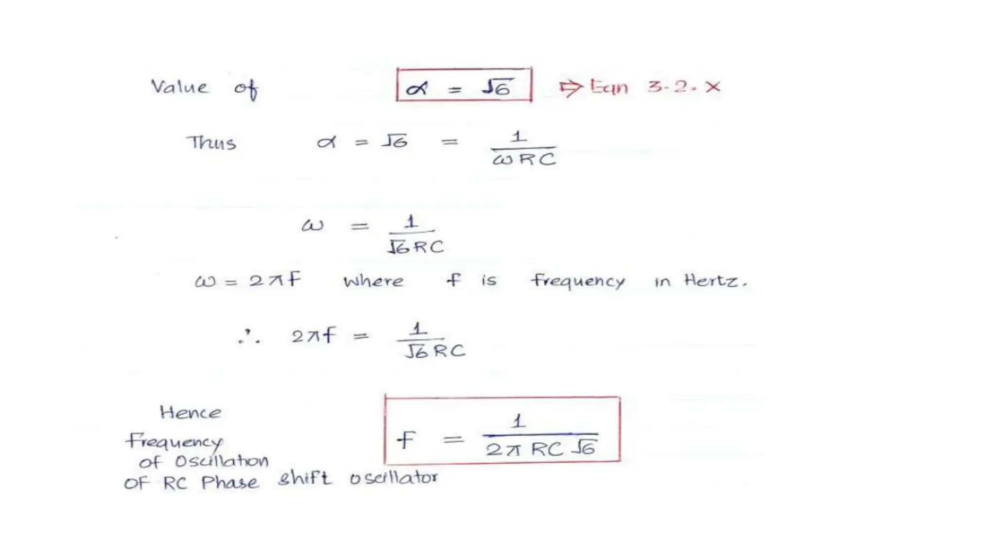
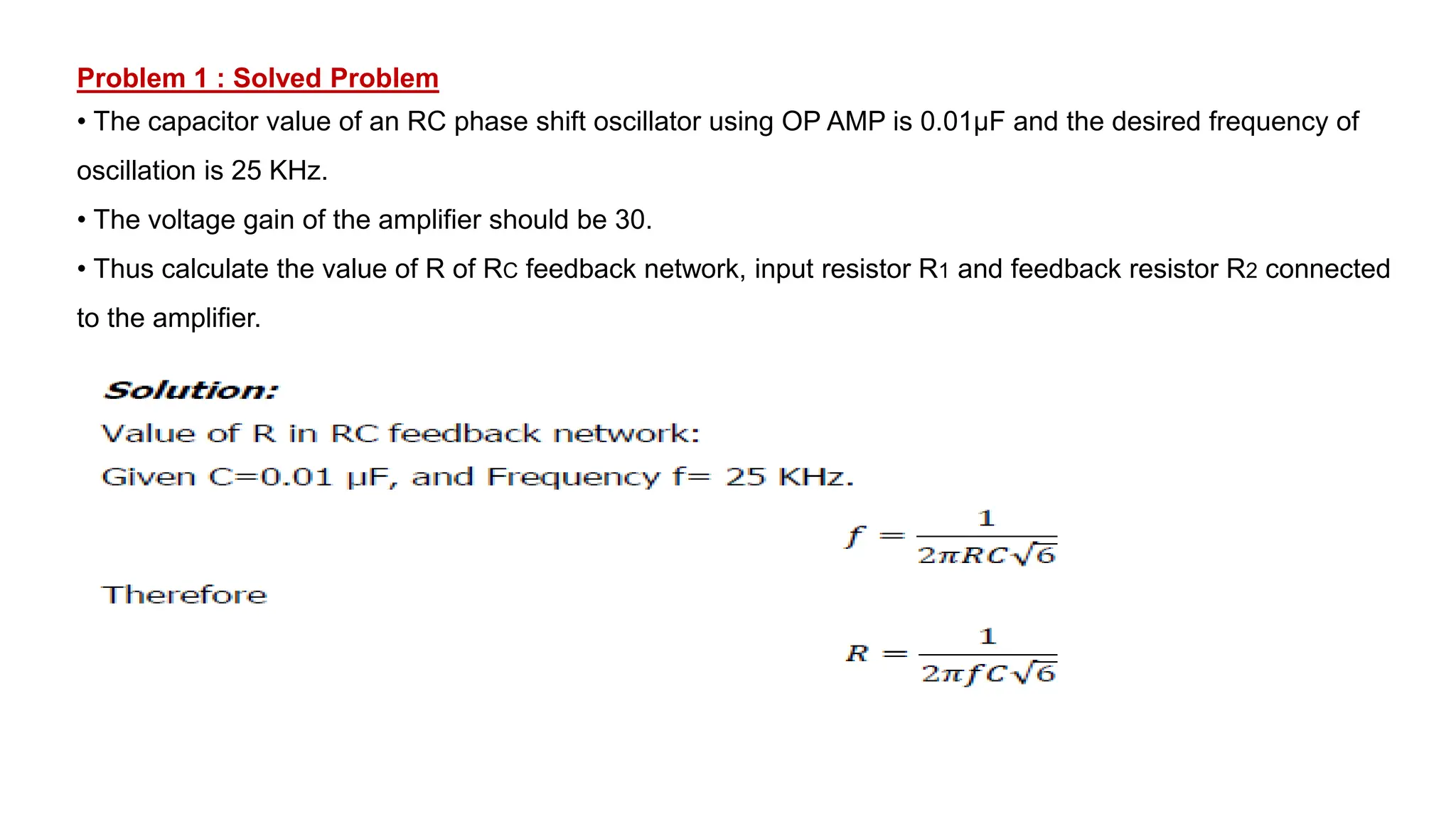
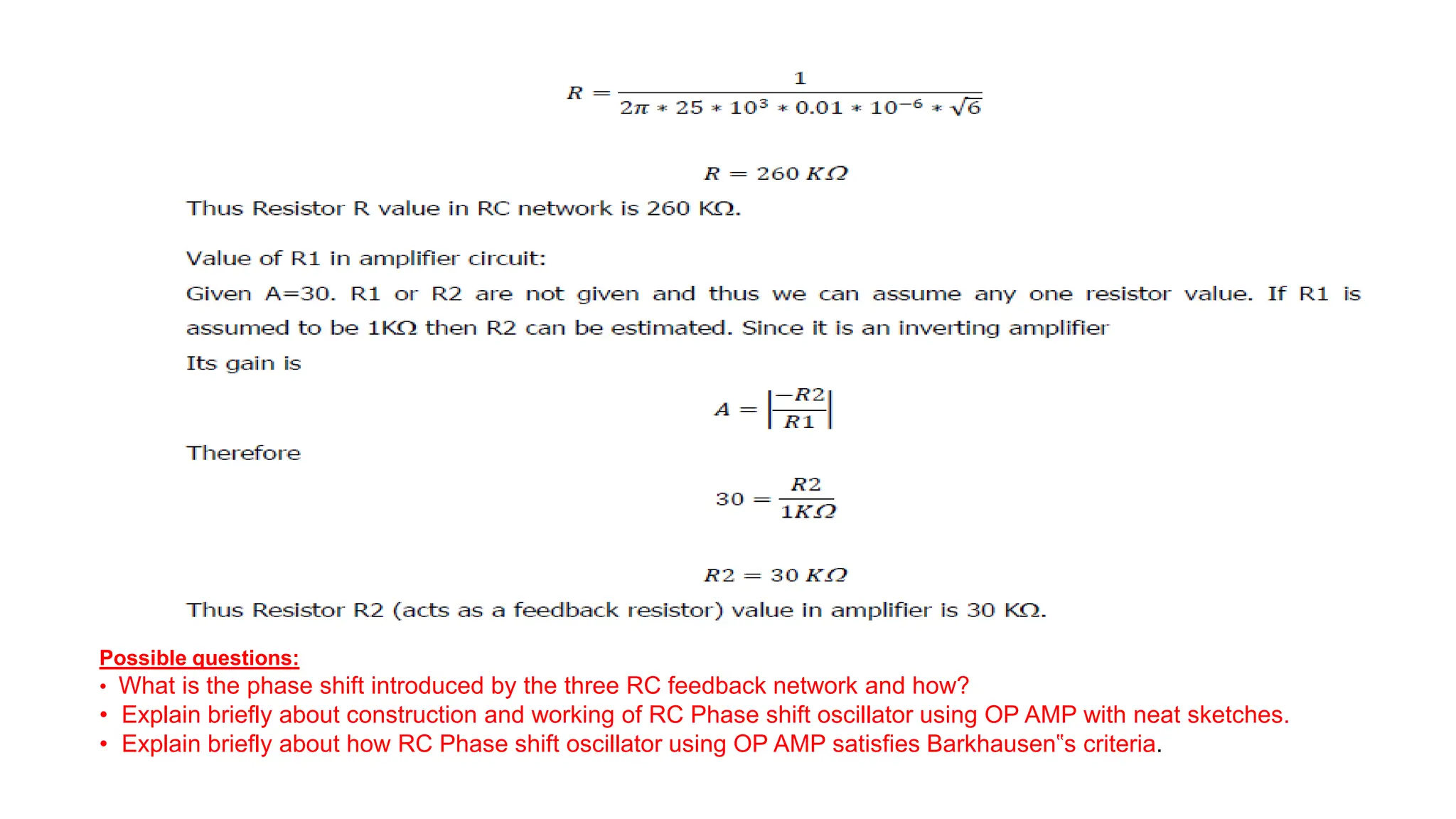
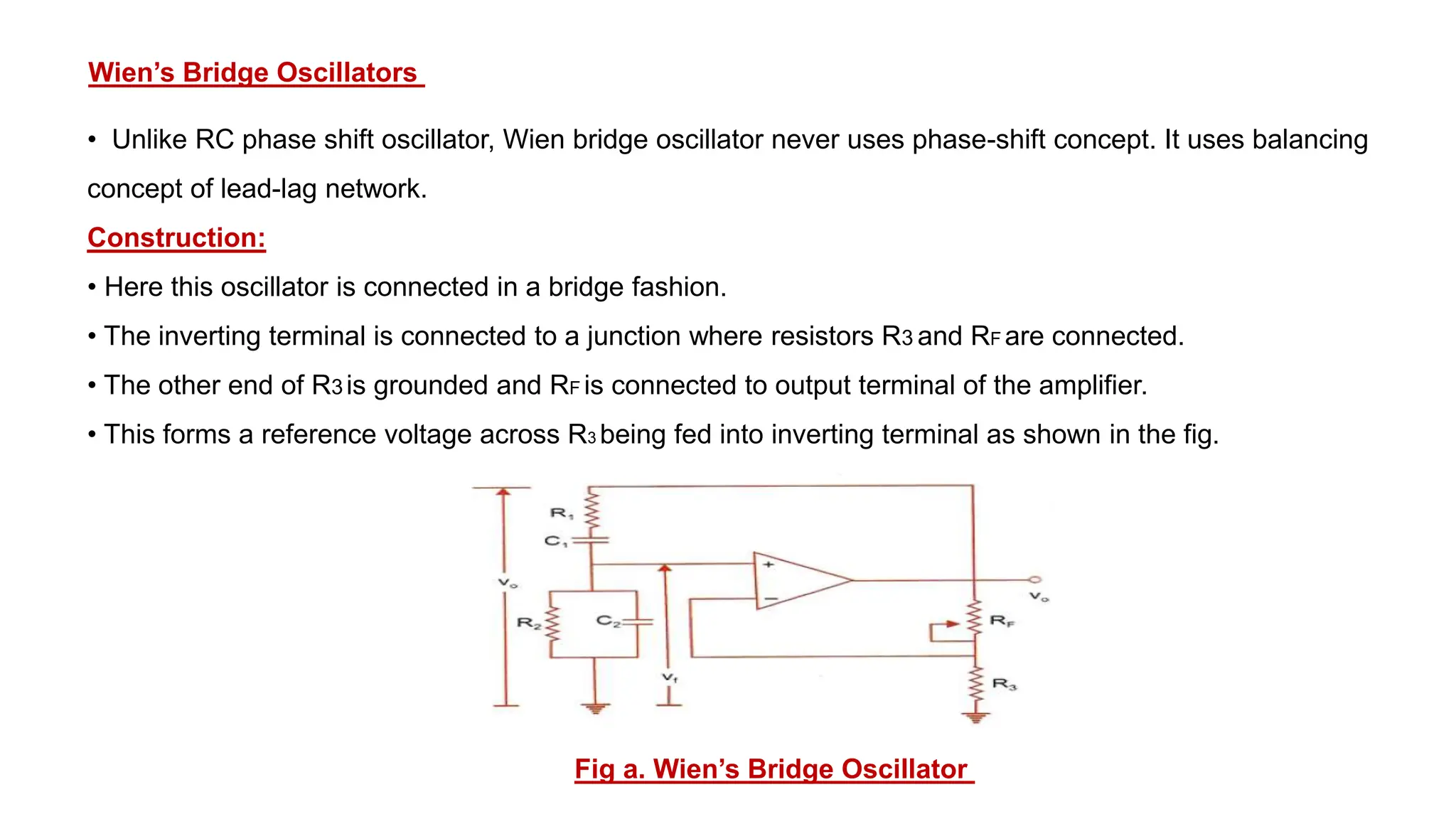
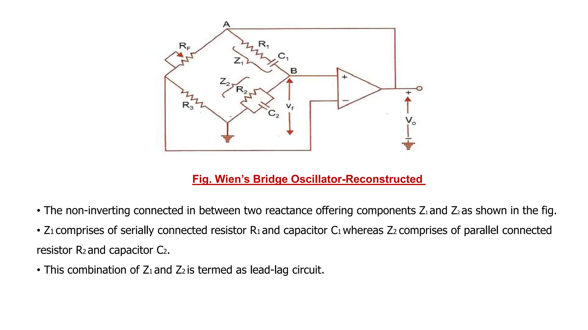
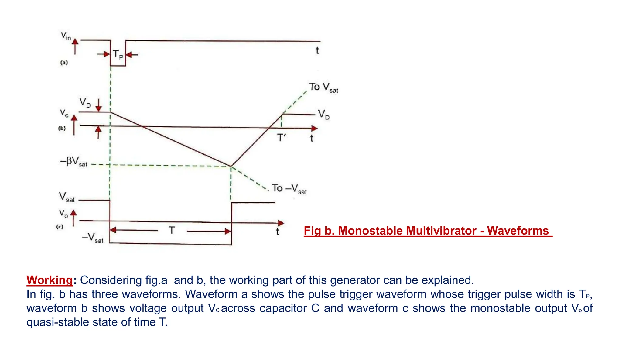
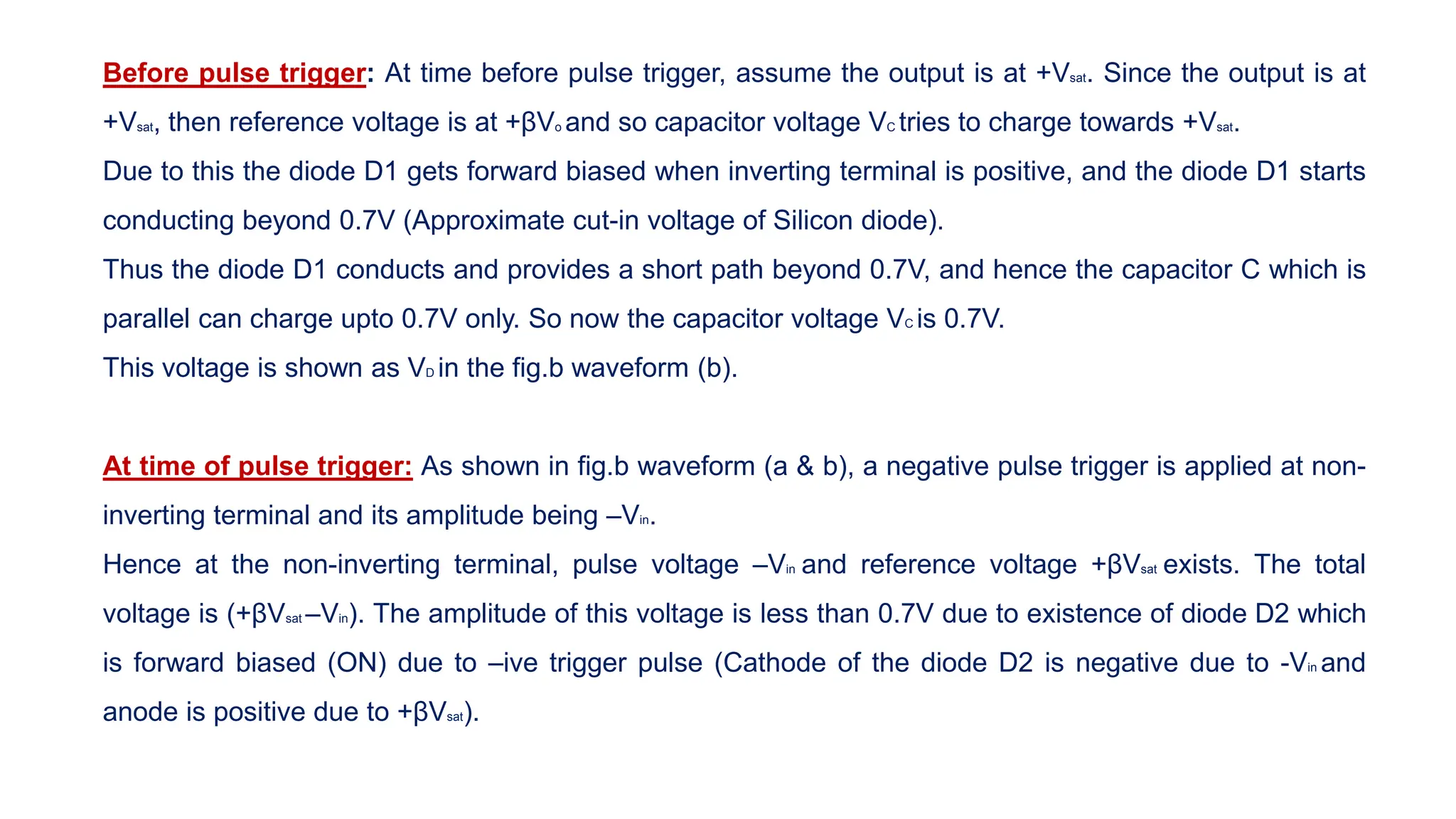
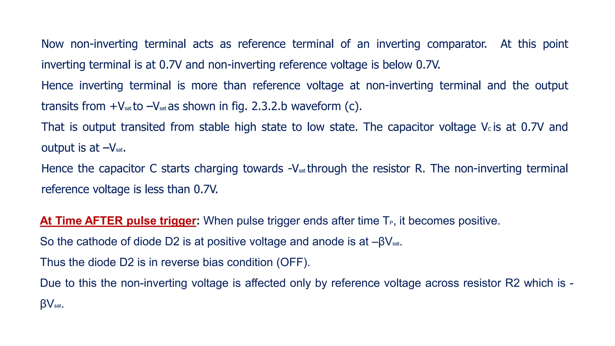
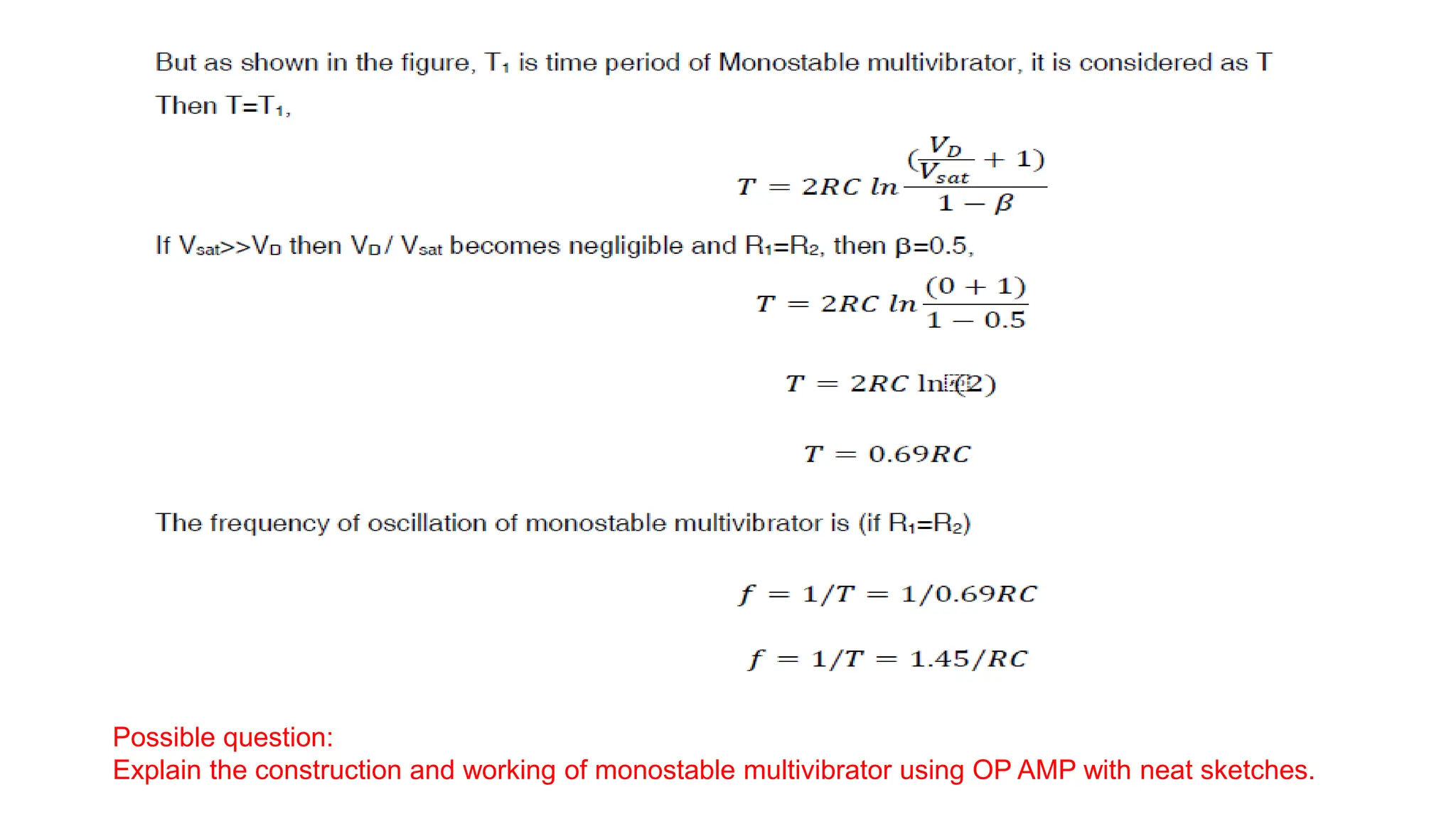
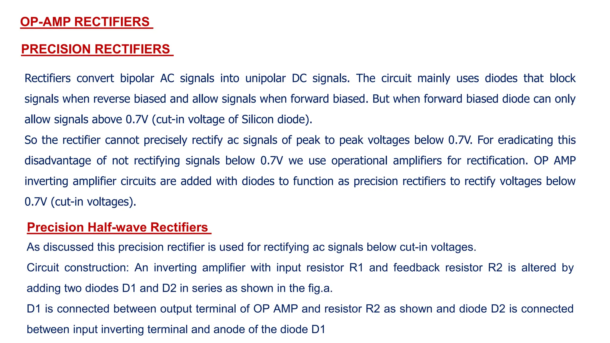
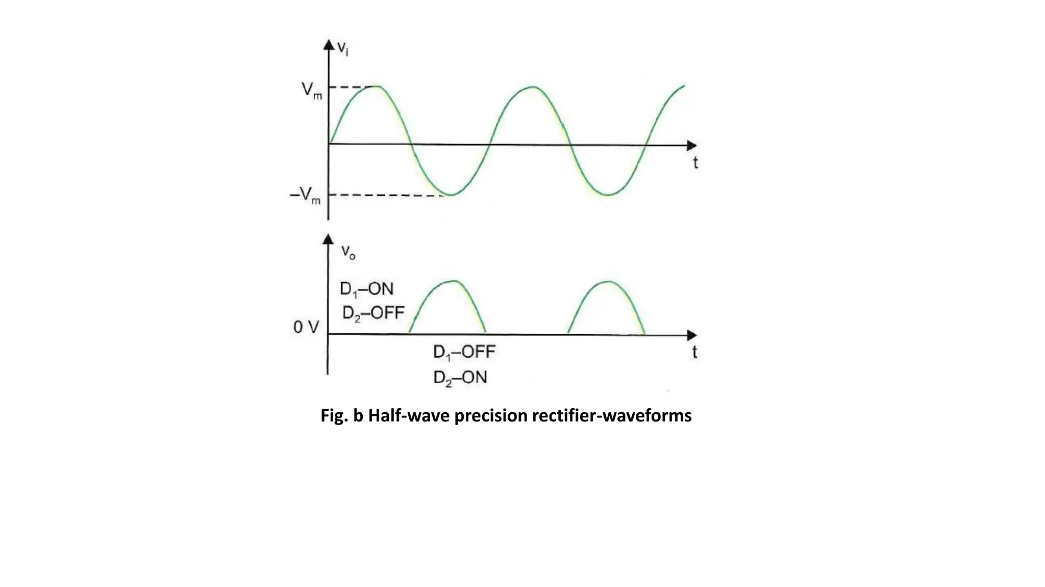
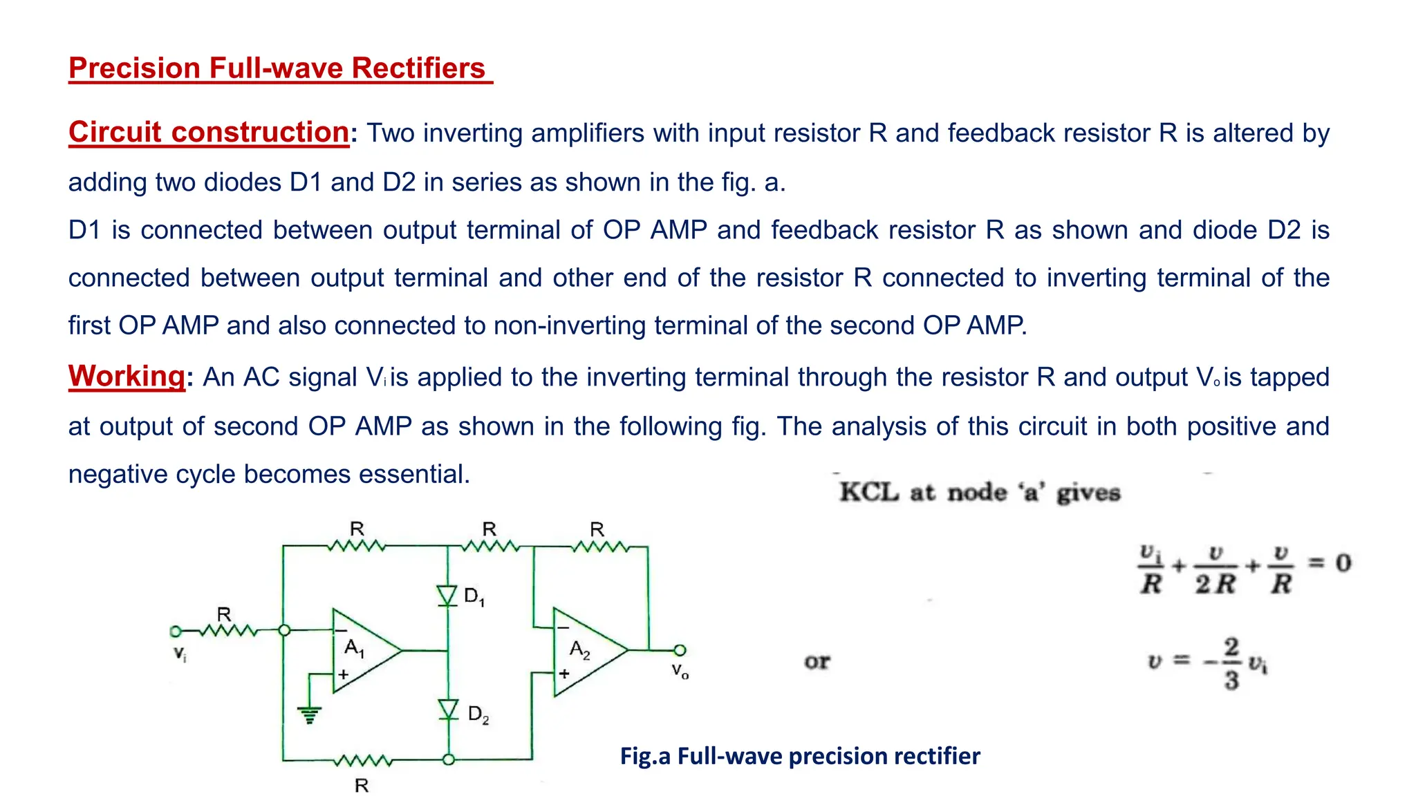
The document discusses the applications of operational amplifiers (op-amps) in various analog circuits, including instrumentation amplifiers, log and antilog amplifiers, comparators, and oscillators. It outlines key features, circuit designs, and operational principles of these components, emphasizing their significance in measuring and controlling physical quantities in industrial and consumer applications. Additionally, it explores concepts such as hysteresis in comparators and Barkhausen's criteria for sustained oscillations in oscillators.


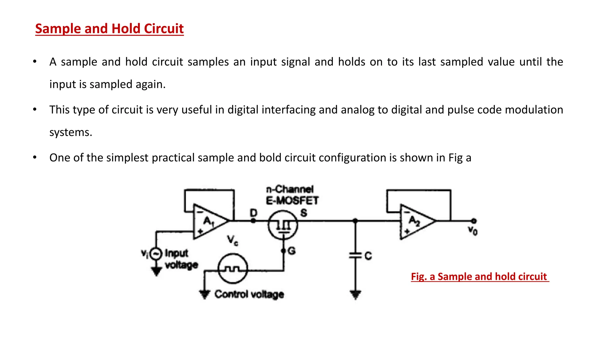
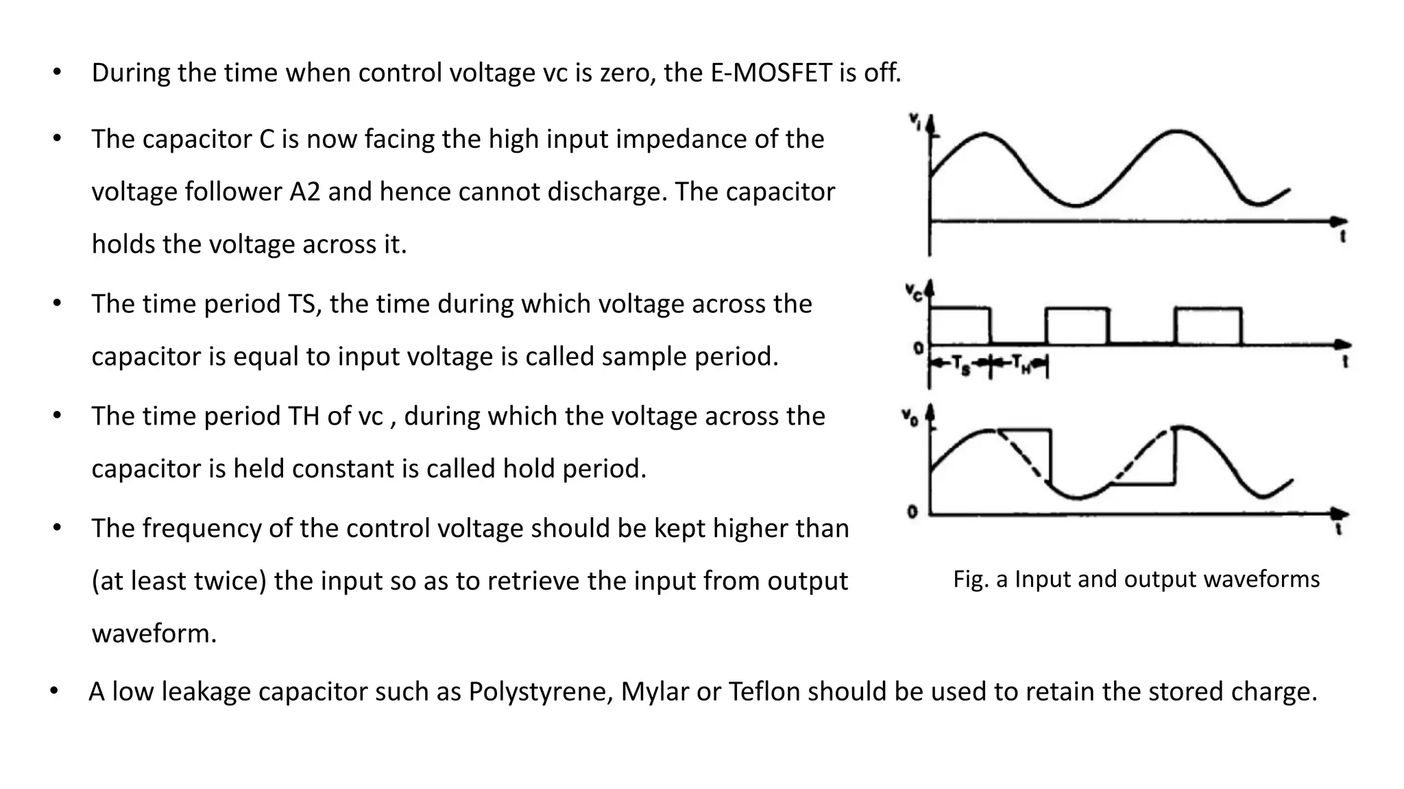
![• The n-channel E-MOSFET works as a switch and is controlled by the control voltage Vc and the
capacitor C stores the charge.
• The analog signal Vi to be sampled is applied to the drain of E-MOSFET and the control voltage Vc
is applied to its gate.
• When Vc is positive, the E-MOSFET turns on and the capacitor C charges to the instantaneous
value of input Vi with a time constant [Ro +rDS (on) C]
• Here Ro is the output resistance of the voltage follower A1 and rDS(on) is the resistance of the
MOSFET when on.
• Thus the input voltage vi appears across the capacitor C and then at the output through the
voltage follower A2. The waveforms are as shown in Fig a](https://image.slidesharecdn.com/licetunitiiipptcharateristicsofop-amp-240518125113-53316cf5/75/linear5-circuit-analysis-Charateristics-of-Op-Amp-ppt-101-2048.jpg)