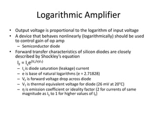
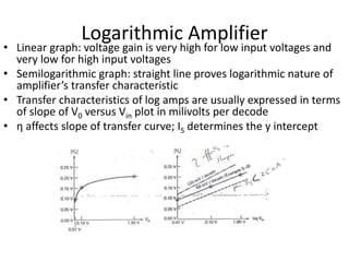
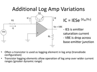
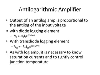
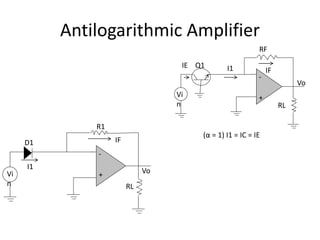
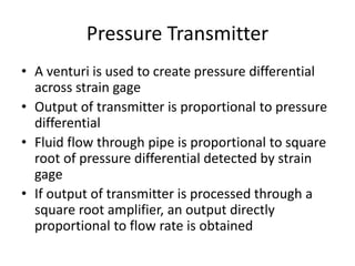
The document discusses nonlinear operational amplifier (op-amp) circuits, focusing on logarithmic and antilogarithmic amplifiers, which are used to manage signals that require nonlinear behavior. It details how devices like silicon diodes and transistors can be utilized in these applications, along with their operational principles and graphical representations. The document also covers mathematical operations using op-amps, precision rectifiers, and active filters, detailing their functionalities and practical implementations in various electronic systems.

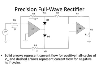
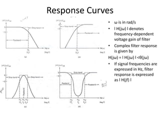
![Basic Log Amp operation
D1
-
+
Vin Vo
RL
R1 IF
I1
• I1 = Vin/R1
• IF = - I1
• IF = - Vin/R1
• V0= -VF = -ηVT ln(IF/IS)
• V0= -ηVT ln[Vin/(R1IS)]
• rD = 26 mV / IF
• IF < 1 mA (log amps)
• At higher current levels (IF > 1 mA) diodes begin to
behave somewhat linearly](https://image.slidesharecdn.com/lic-ch-2-230808055552-3469a33b/85/LIC-CH-2-pptx-3-320.jpg)
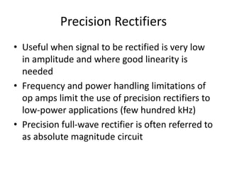
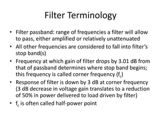
![Precision Full-Wave Rectifier
• Positive half-cycle causes D1 to become forward-
biased, while reverse-biasing D2
– VB = 0 V
– VA = -Vin R2/R1
– Output of U2 is V0 = -VA R5/R4 = Vin (R2R5/R1R4)
• Negative half-cycle causes U1 output positive, forward-
biasing D2 and reverse-biasing D1
– VA = 0 V
– VB = -Vin R3/R1
– Output of U2 (noninverting configuration) is
V0 = VB [1+ (R5/R4)]= - Vin [(R3/R1)+(R3R5/R1R4)
– if R3 = R1/2, both half-cycles will receive equal gain](https://image.slidesharecdn.com/lic-ch-2-230808055552-3469a33b/85/LIC-CH-2-pptx-19-320.jpg)

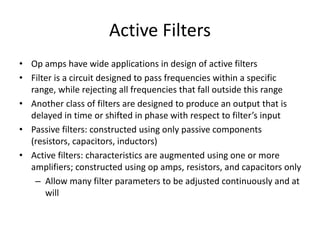
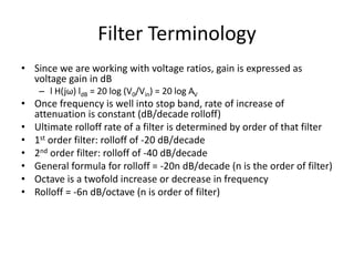
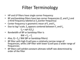
![Filter Terminology
• Decibel voltage gain is actually intended to be
logarithmic representation of power gain
• Power gain is related to decibel voltage gain as
– AP = 10 log (P0/Pin)
– P0 = (V0
2/ZL) and Pin = (Vin
2/Zin)
– AP = 10 log [(V0
2/ZL) /(Vin
2/Zin)]
– AP = 10 log (V0
2Zin /Vin
2ZL)]
– If ZL = Zin, AP = 10 log (V0
2/Vin
2) = 10 log (V0/Vin)2
– AP = 20 log (V0/Vin) = 20 log Av
• When input impedance of filter equals impedance of
load being driven by filter, power gain is dependent on
voltage gain of circuit only](https://image.slidesharecdn.com/lic-ch-2-230808055552-3469a33b/85/LIC-CH-2-pptx-26-320.jpg)
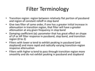
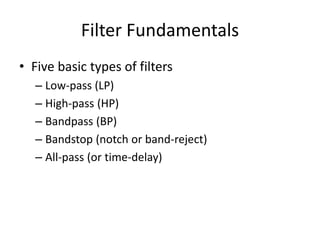
![Basic Filter Theory Review
• Simplest filters are 1st order LP and HP RC sections
– Passband gain slightly less than unity
• Assuming neglegible loading, amplitude response (voltage
gain) of LP section is
H(jω) = (jXC) / (R + jXC)
H(jω) = XC/sqrt(R2+XC
2) <-tan-1 (R/XC)
• Corner frequency fc for 1st order LP or HP RC section is
found by making R = XC and solving for frequency
R = XC = 1/(2πfC)
1/fC = 2πRC
fC = 1/(2πRC)
• Gain (in dB) and phase response of 1st order LP
H(jf) dB = 20 log [1/{sqrt(1+(f/fc)2}] <-tan-1 (f/fC)
• Gain (in dB) and phase response of 1st order HP
H(jf) dB = 20 log [1/{sqrt(1+(fc/f)2}] <tan-1 (fC/f)
Operational Amplifiers and Linear
Integrated Circuits: Theory and Applications
by Denton J. Dailey
For more detail contact us](https://image.slidesharecdn.com/lic-ch-2-230808055552-3469a33b/85/LIC-CH-2-pptx-31-320.jpg)


