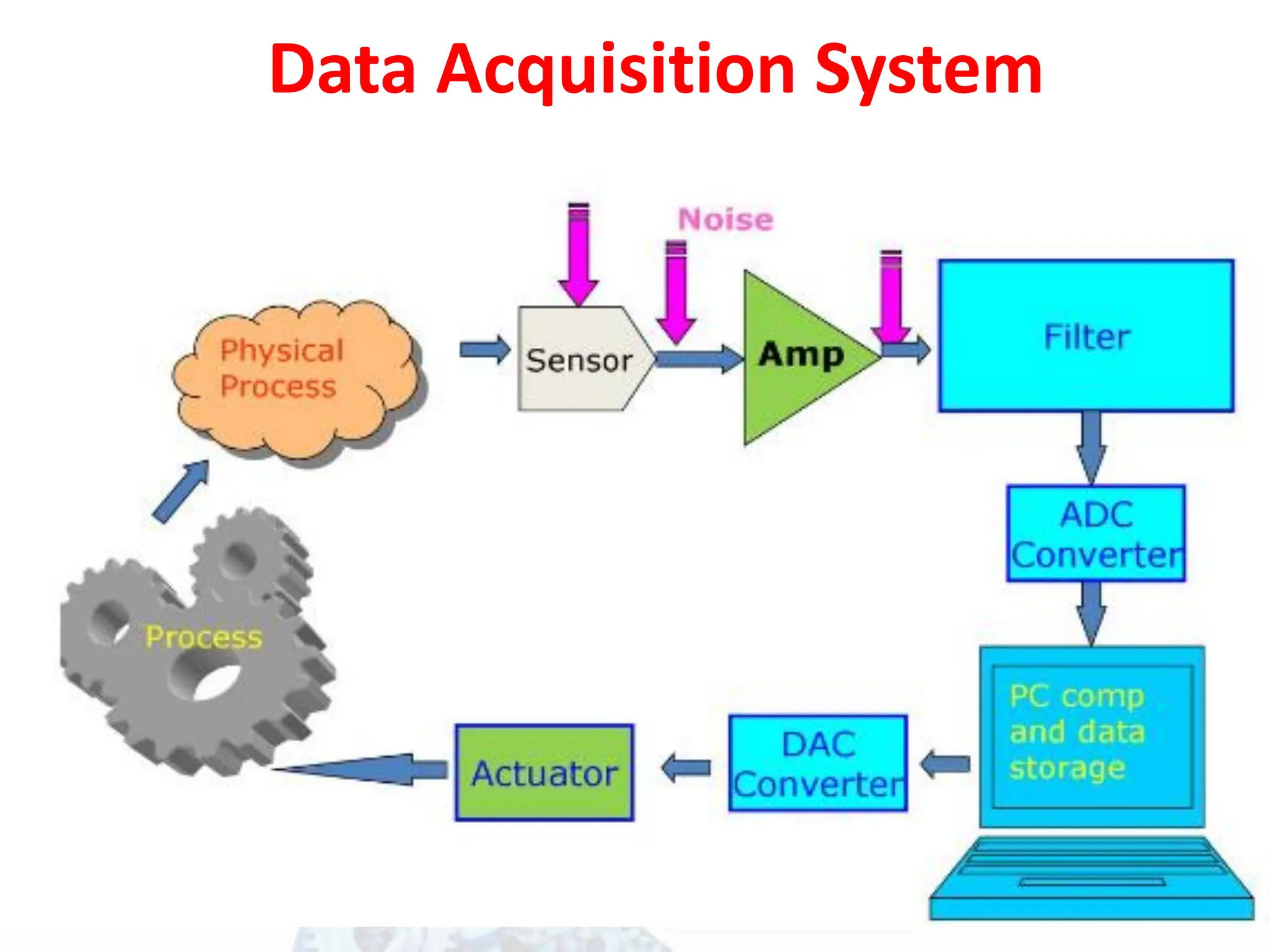
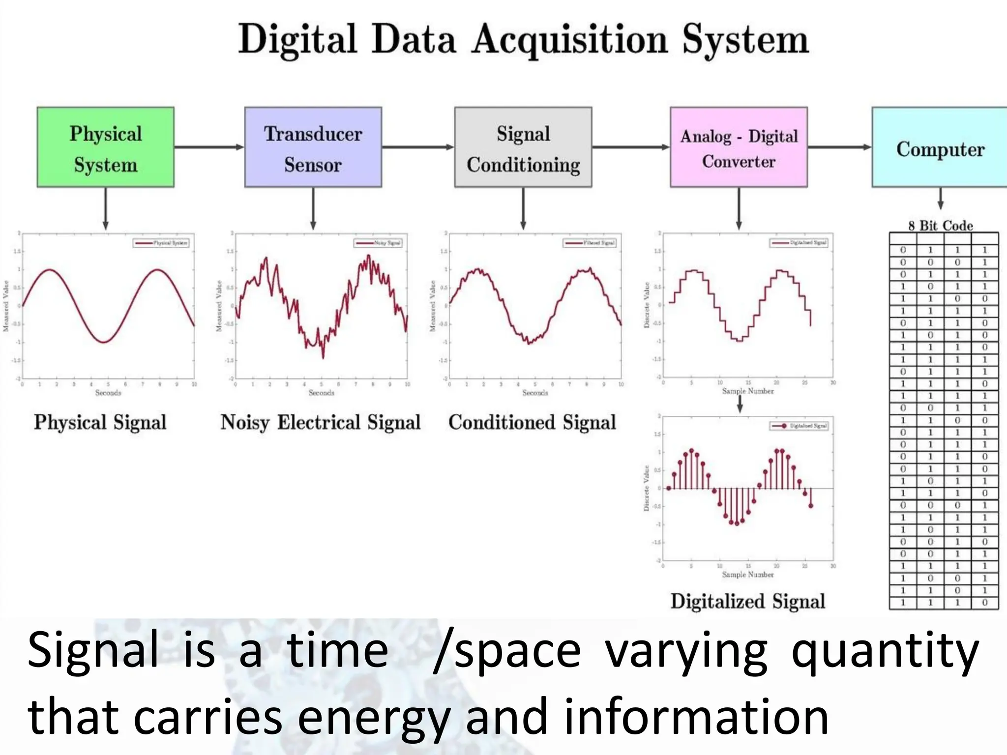
Signal is atime /space varying quantity
that carries energy and information
4.
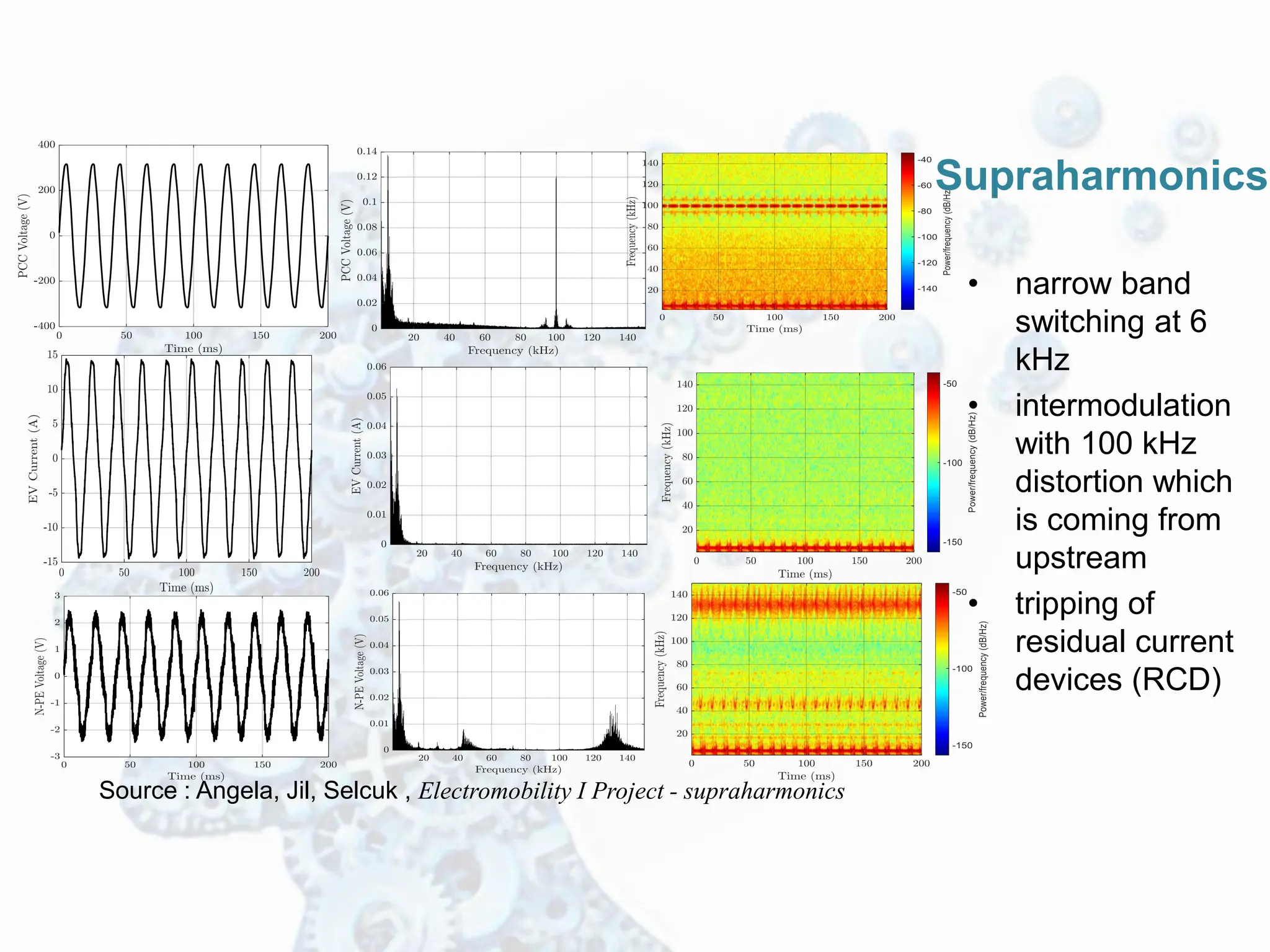
• narrow band
switchingat 6
kHz
• intermodulation
with 100 kHz
distortion which
is coming from
upstream
• tripping of
residual current
devices (RCD)
Source : Angela, Jil, Selcuk , Electromobility I Project - supraharmonics
Supraharmonics
5.
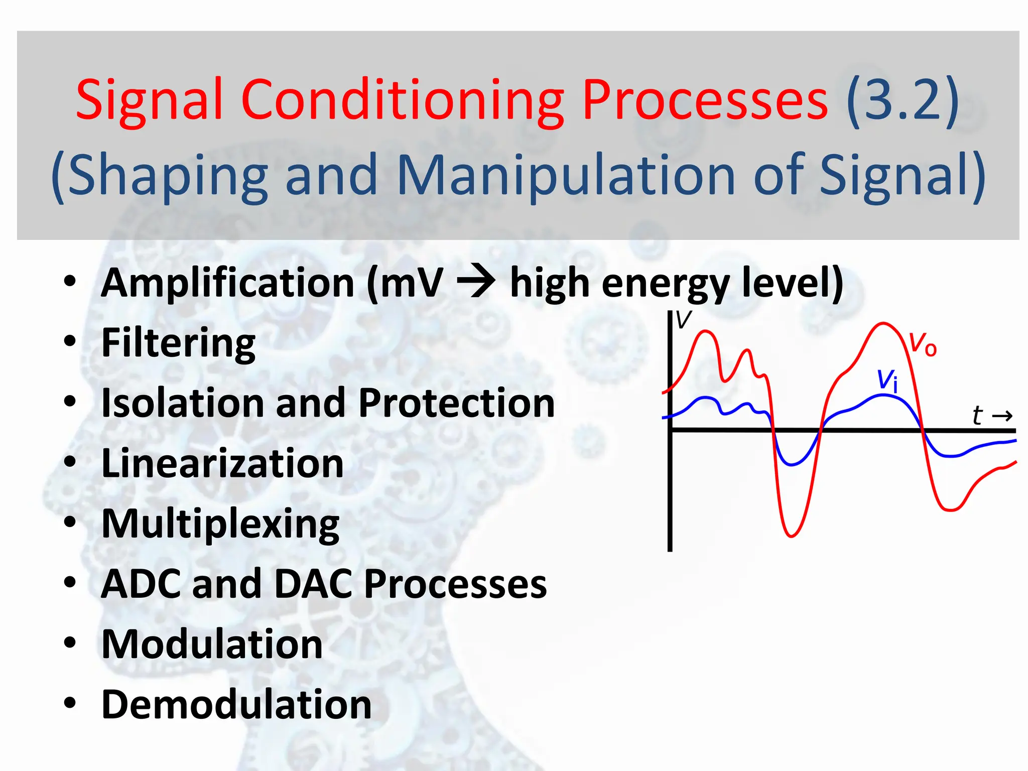
• Amplification (mV→ high energy level)
• Filtering
• Isolation and Protection
• Linearization
• Multiplexing
• ADC and DAC Processes
• Modulation
• Demodulation
Signal Conditioning Processes (3.2)
(Shaping and Manipulation of Signal)
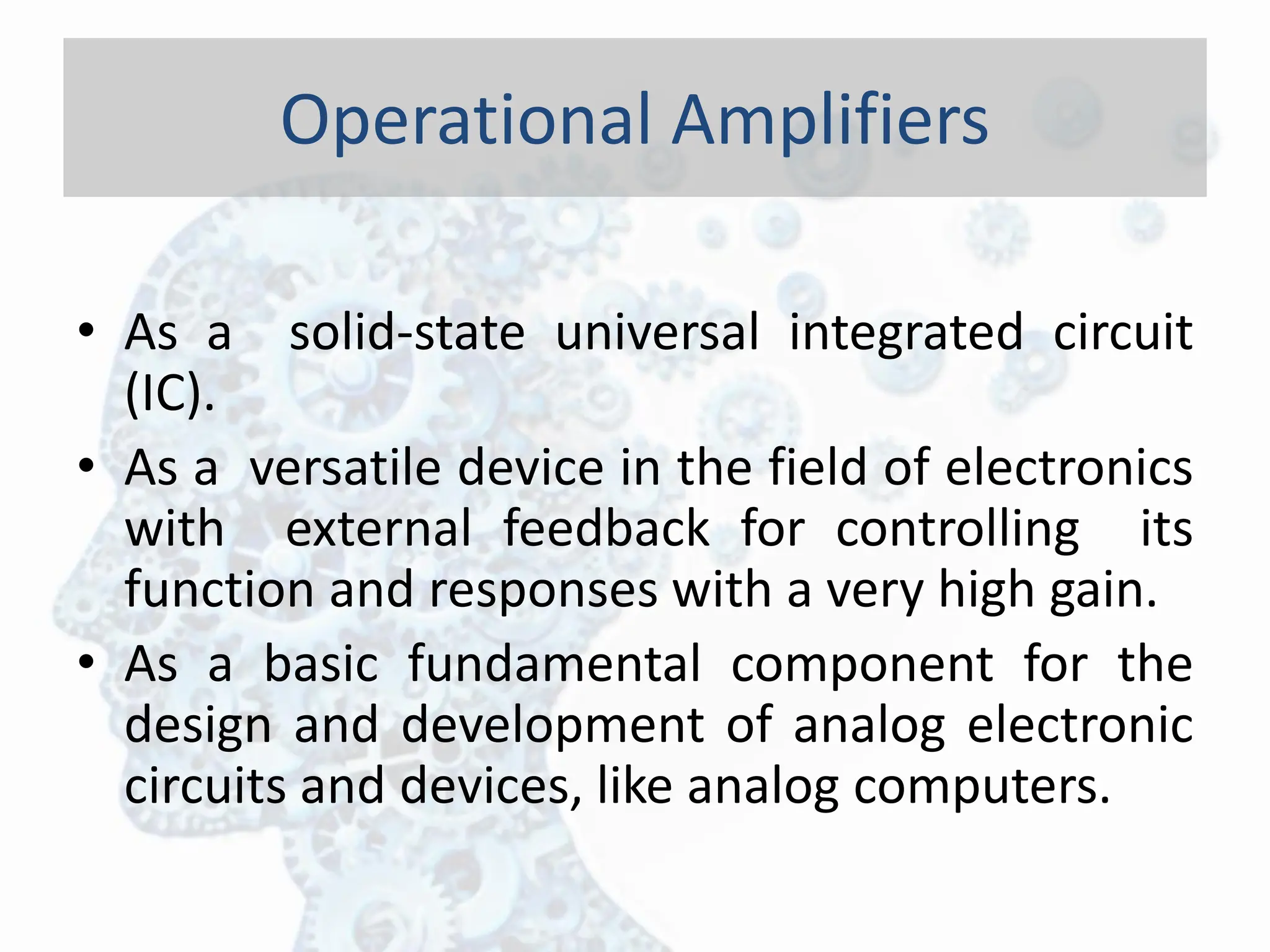
• As asolid-state universal integrated circuit
(IC).
• As a versatile device in the field of electronics
with external feedback for controlling its
function and responses with a very high gain.
• As a basic fundamental component for the
design and development of analog electronic
circuits and devices, like analog computers.
Operational Amplifiers
8.
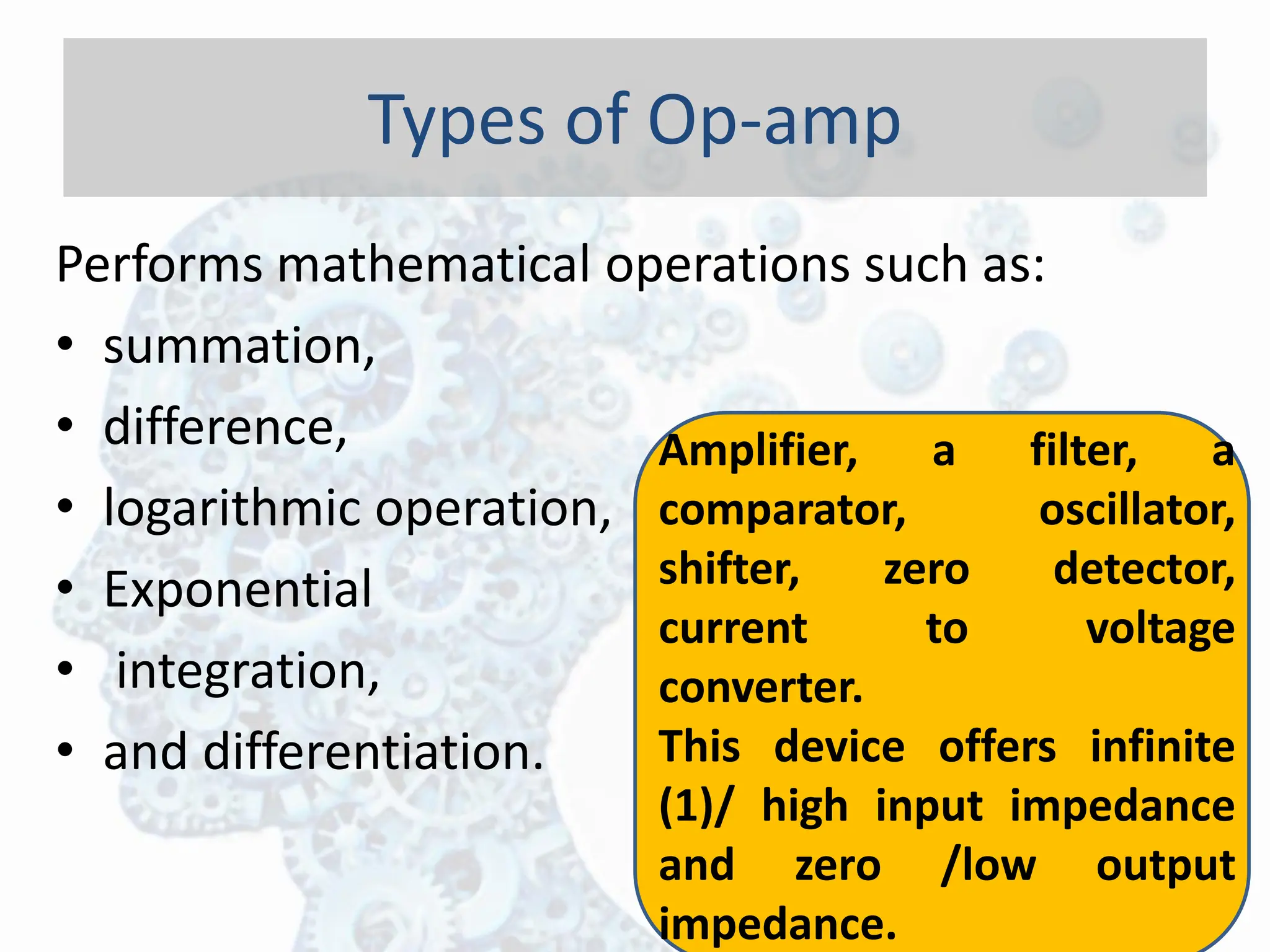
Performs mathematical operationssuch as:
• summation,
• difference,
• logarithmic operation,
• Exponential
• integration,
• and differentiation.
Types of Op-amp
Amplifier, a filter, a
comparator, oscillator,
shifter, zero detector,
current to voltage
converter.
This device offers infinite
(1)/ high input impedance
and zero /low output
impedance.
9.
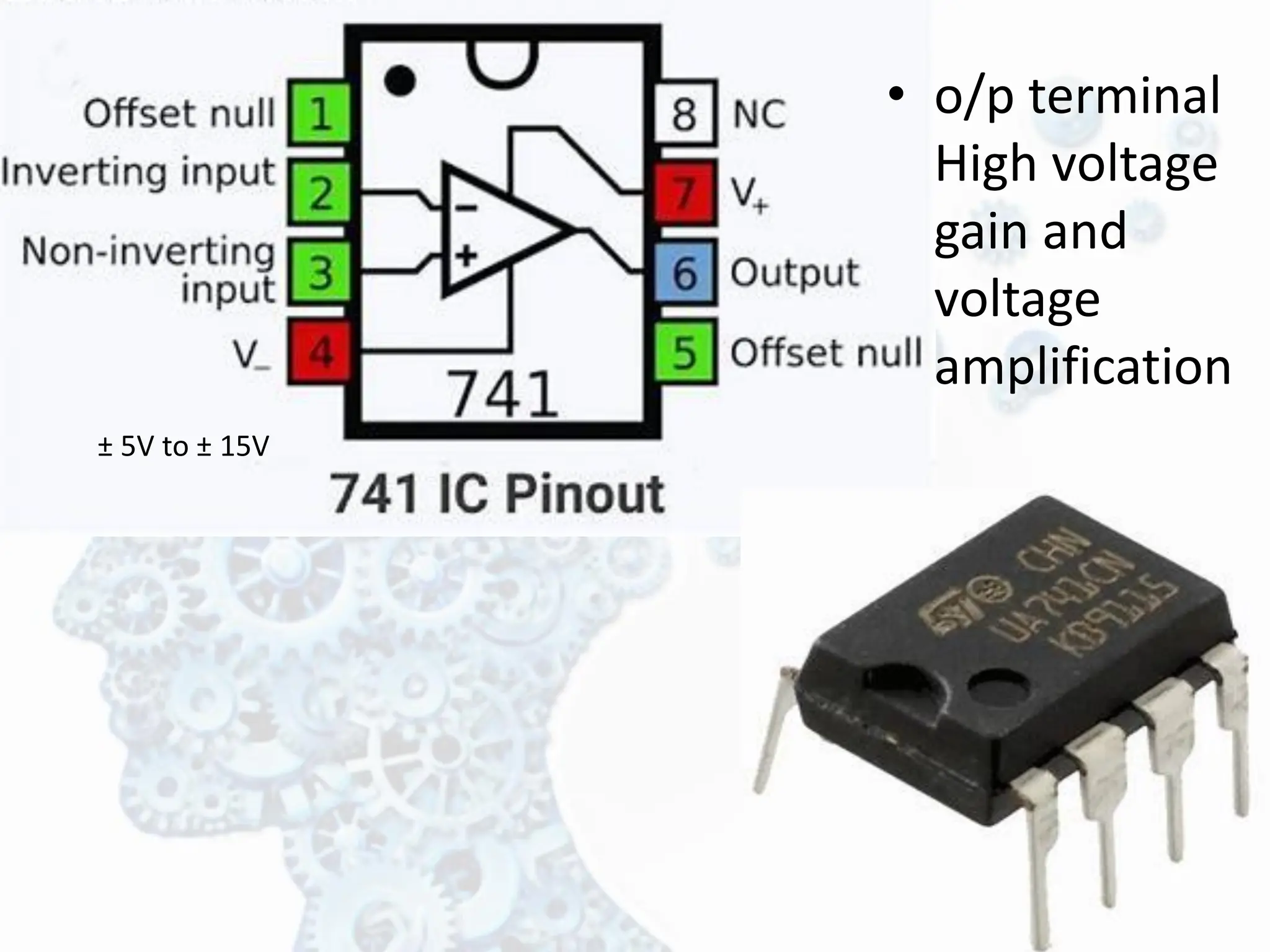
± 5V to± 15V
• o/p terminal
High voltage
gain and
voltage
amplification
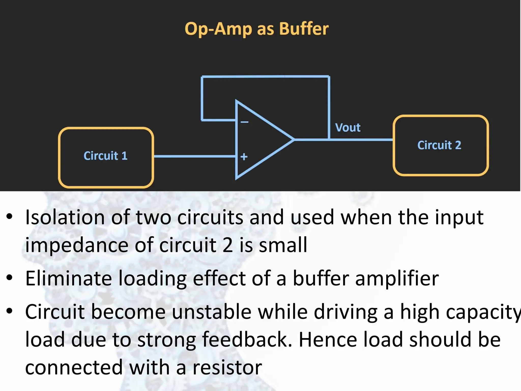
• Isolation oftwo circuits and used when the input
impedance of circuit 2 is small
• Eliminate loading effect of a buffer amplifier
• Circuit become unstable while driving a high capacity
load due to strong feedback. Hence load should be
connected with a resistor
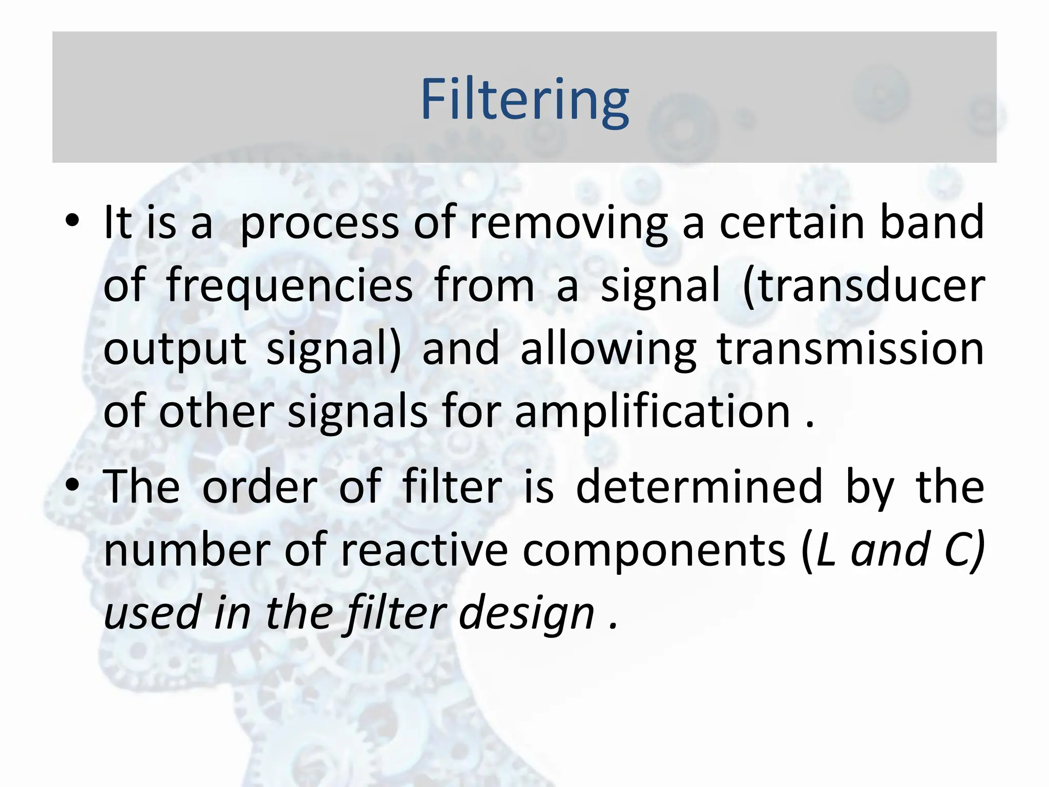
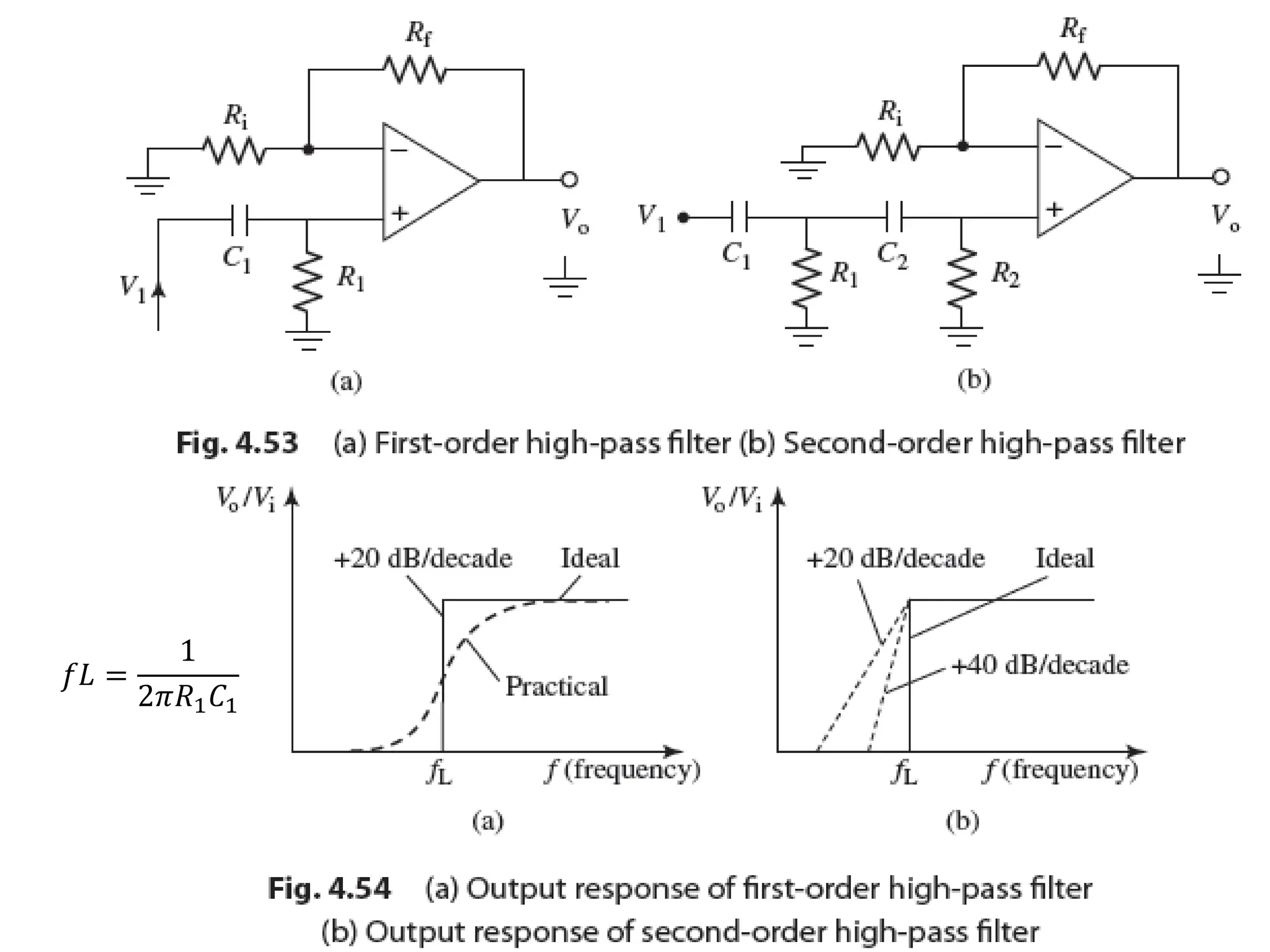
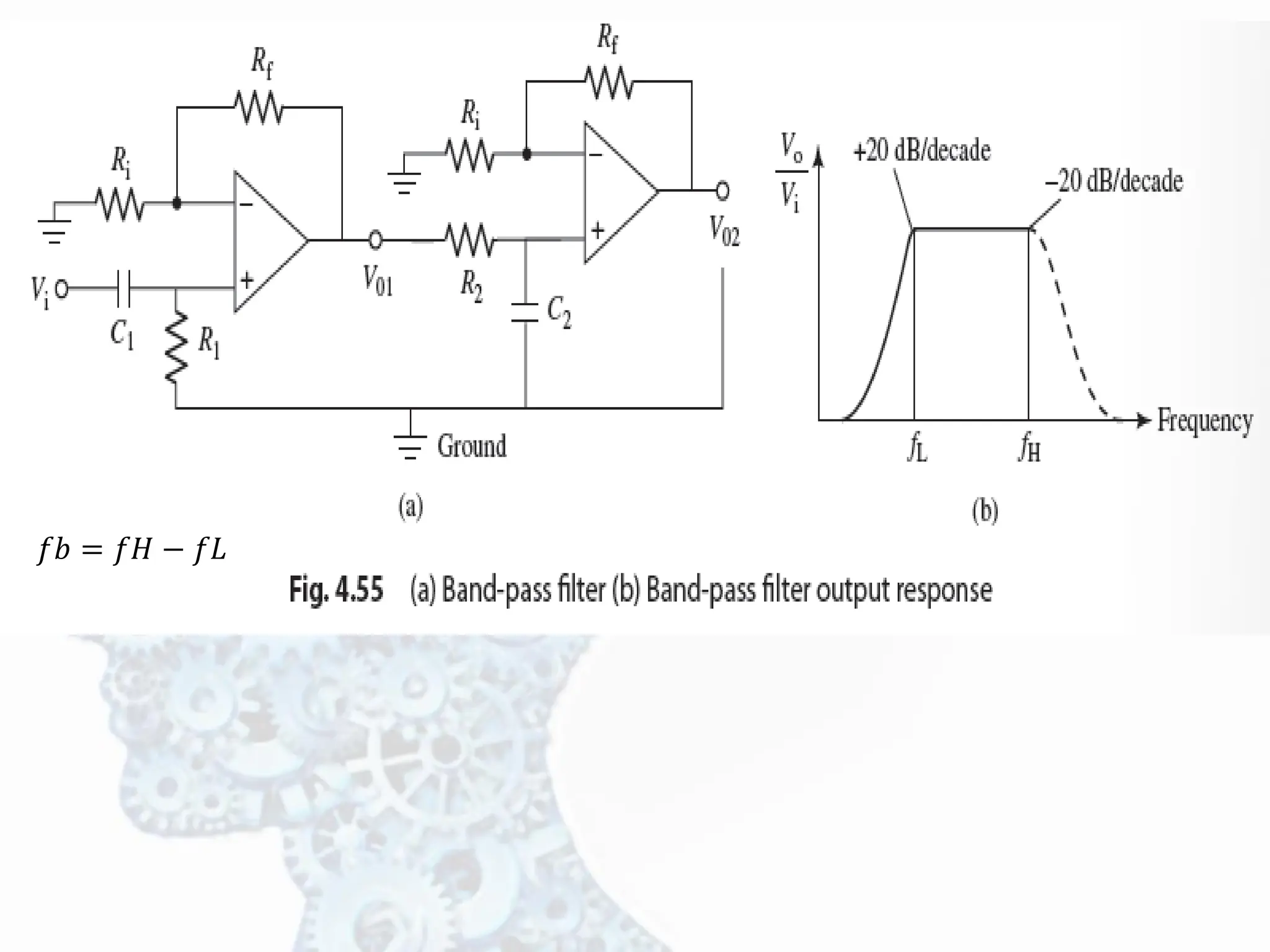
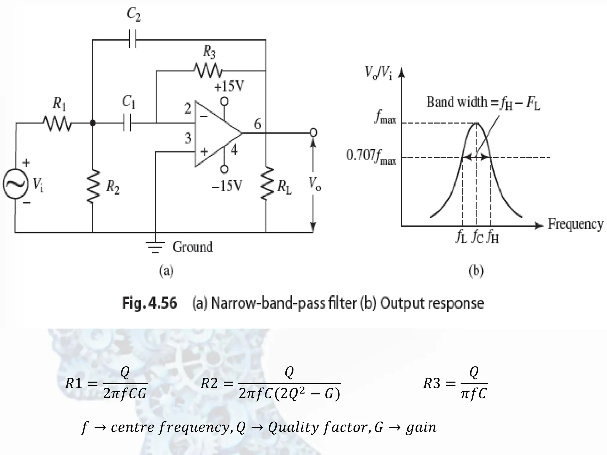
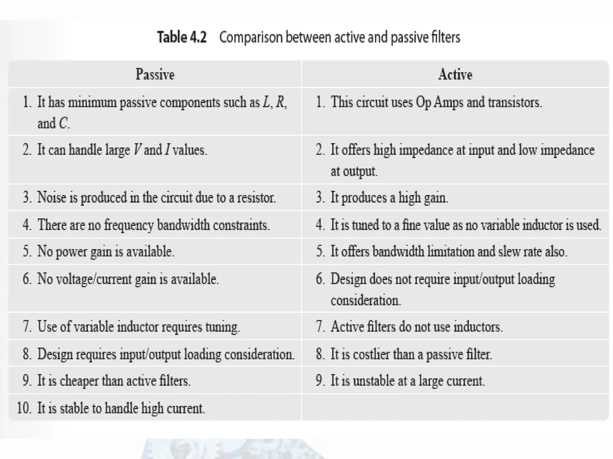
• It isa process of removing a certain band
of frequencies from a signal (transducer
output signal) and allowing transmission
of other signals for amplification .
• The order of filter is determined by the
number of reactive components (L and C)
used in the filter design .
Filtering
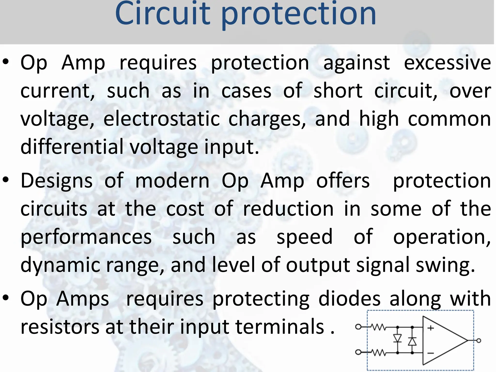
• Op Amprequires protection against excessive
current, such as in cases of short circuit, over
voltage, electrostatic charges, and high common
differential voltage input.
• Designs of modern Op Amp offers protection
circuits at the cost of reduction in some of the
performances such as speed of operation,
dynamic range, and level of output signal swing.
• Op Amps requires protecting diodes along with
resistors at their input terminals .
Circuit protection
41.
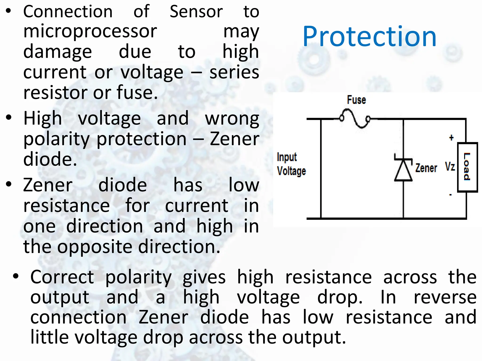
Protection
• Connection ofSensor to
microprocessor may
damage due to high
current or voltage – series
resistor or fuse.
• High voltage and wrong
polarity protection – Zener
diode.
• Zener diode has low
resistance for current in
one direction and high in
the opposite direction.
• Correct polarity gives high resistance across the
output and a high voltage drop. In reverse
connection Zener diode has low resistance and
little voltage drop across the output.
42.
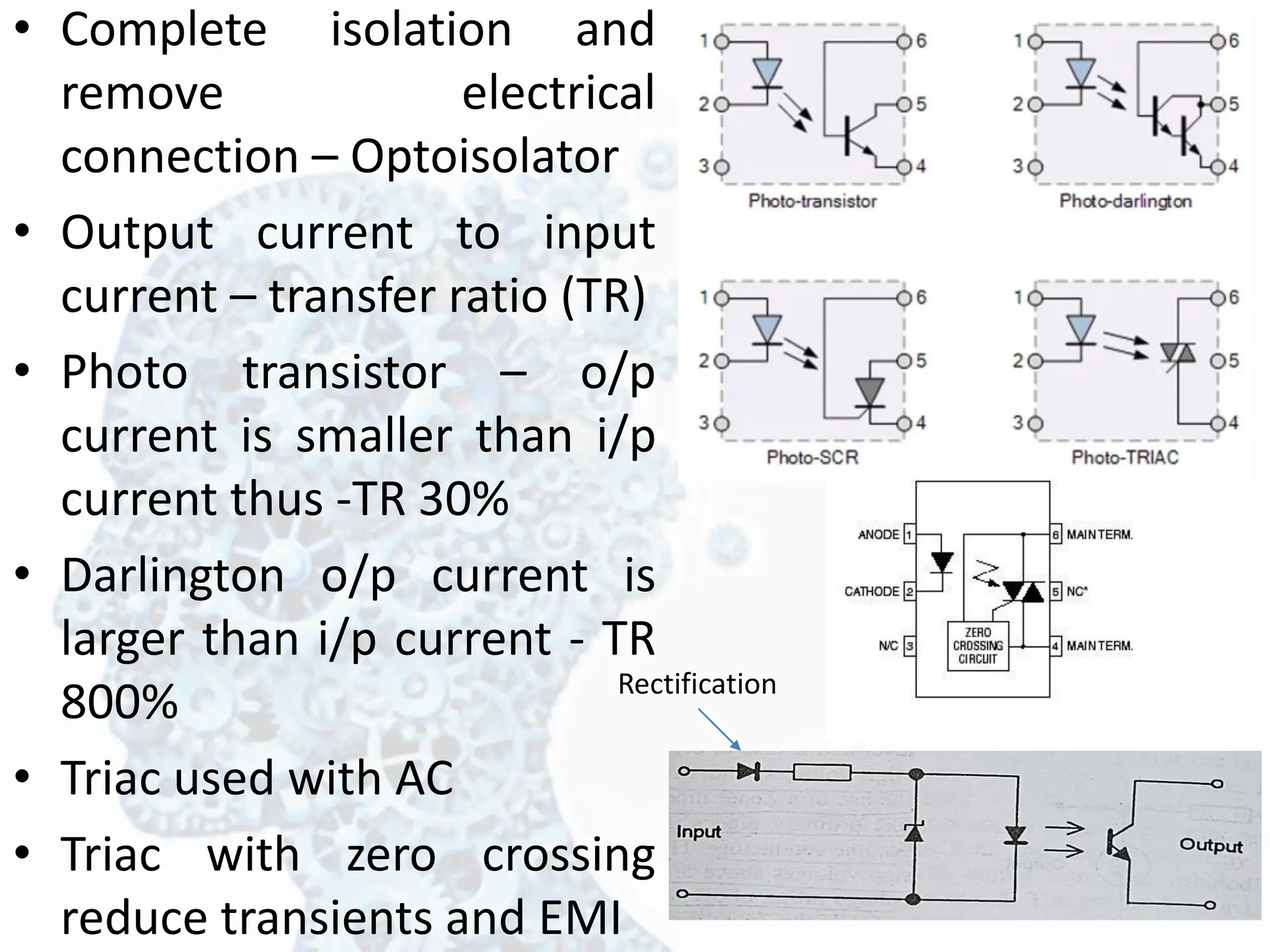
• Complete isolationand
remove electrical
connection – Optoisolator
• Output current to input
current – transfer ratio (TR)
• Photo transistor – o/p
current is smaller than i/p
current thus -TR 30%
• Darlington o/p current is
larger than i/p current - TR
800%
• Triac used with AC
• Triac with zero crossing
reduce transients and EMI
Rectification
43.
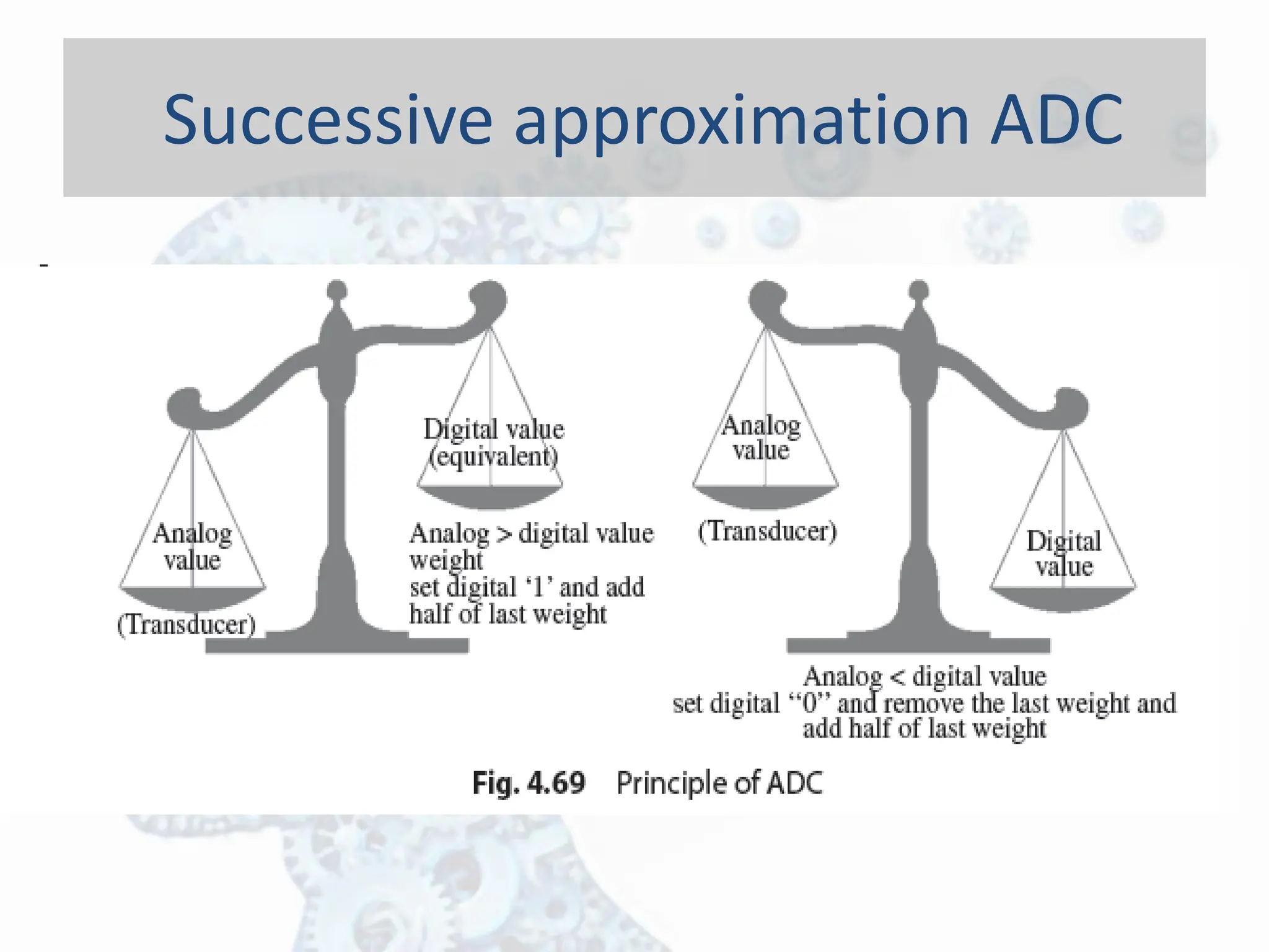
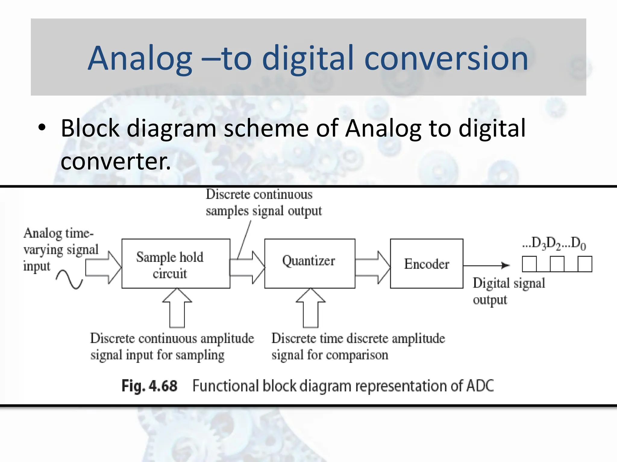
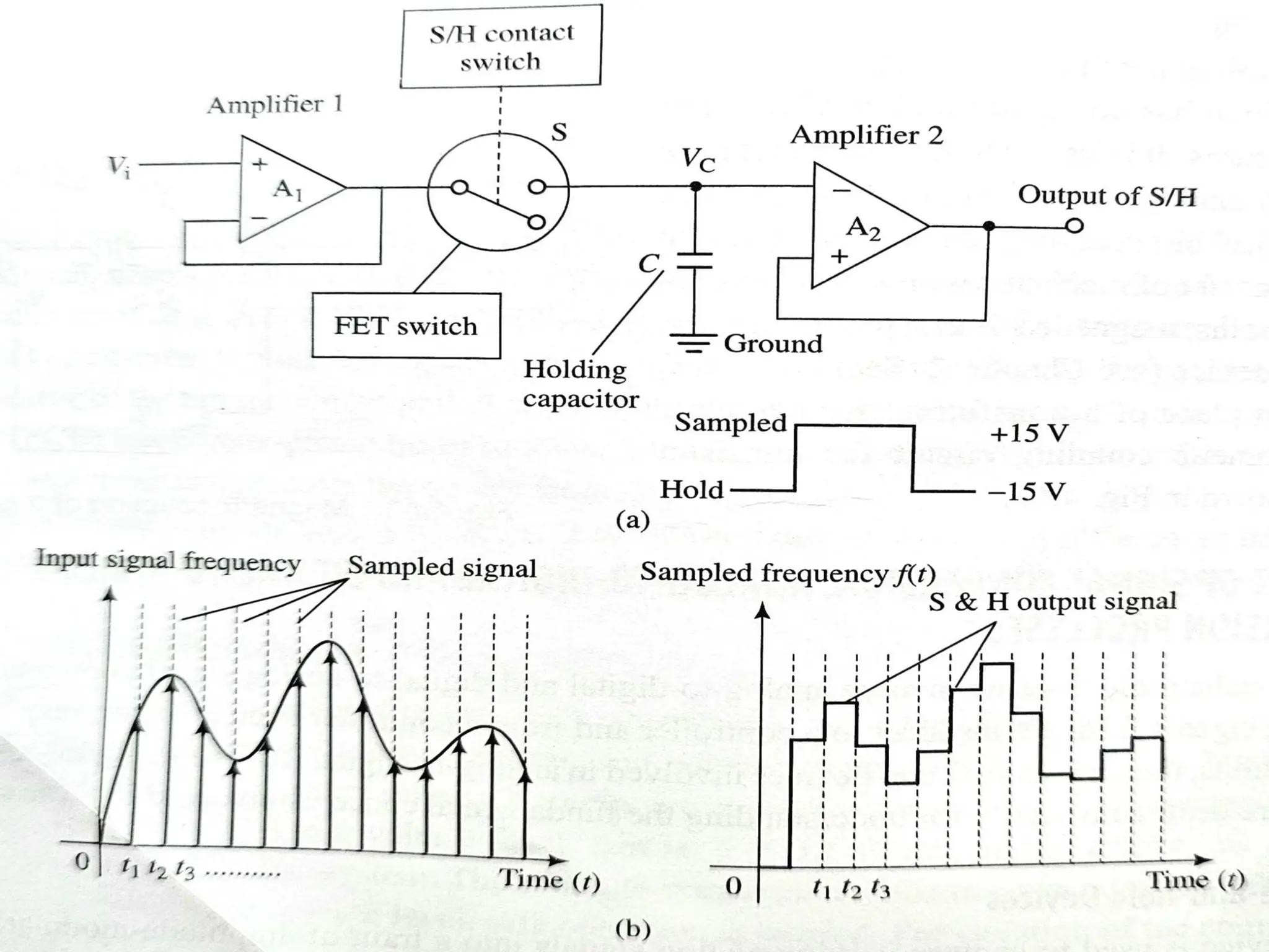
Analog –to digitalconversion
• Block diagram scheme of Analog to digital
converter.
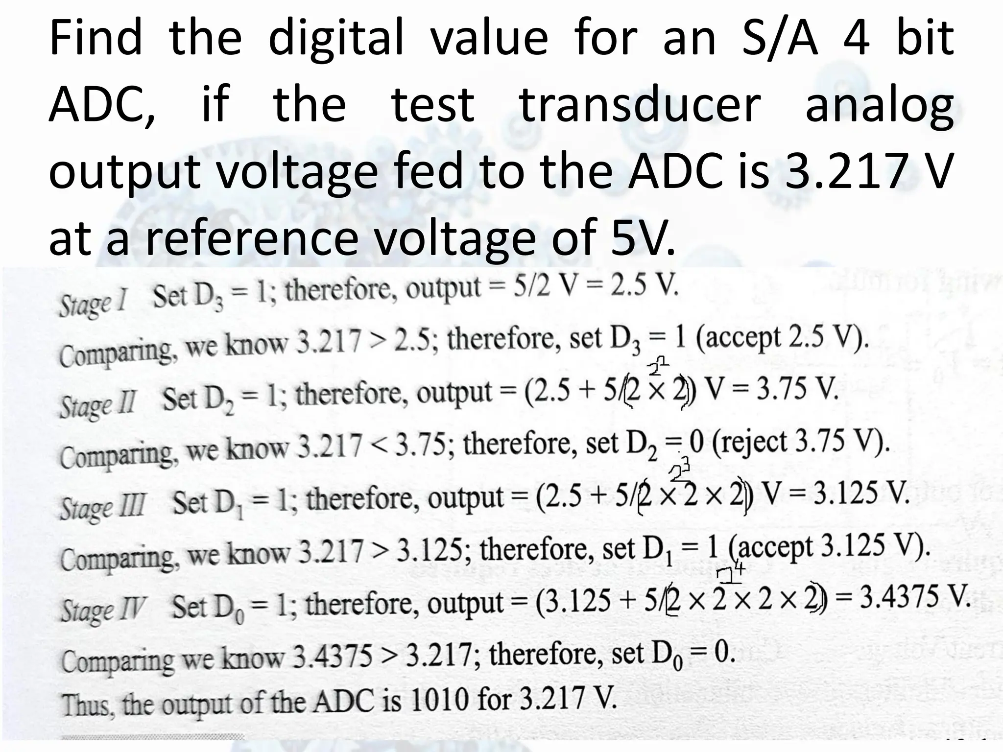
Find the digitalvalue for an S/A 4 bit
ADC, if the test transducer analog
output voltage fed to the ADC is 3.217 V
at a reference voltage of 5V.
49.
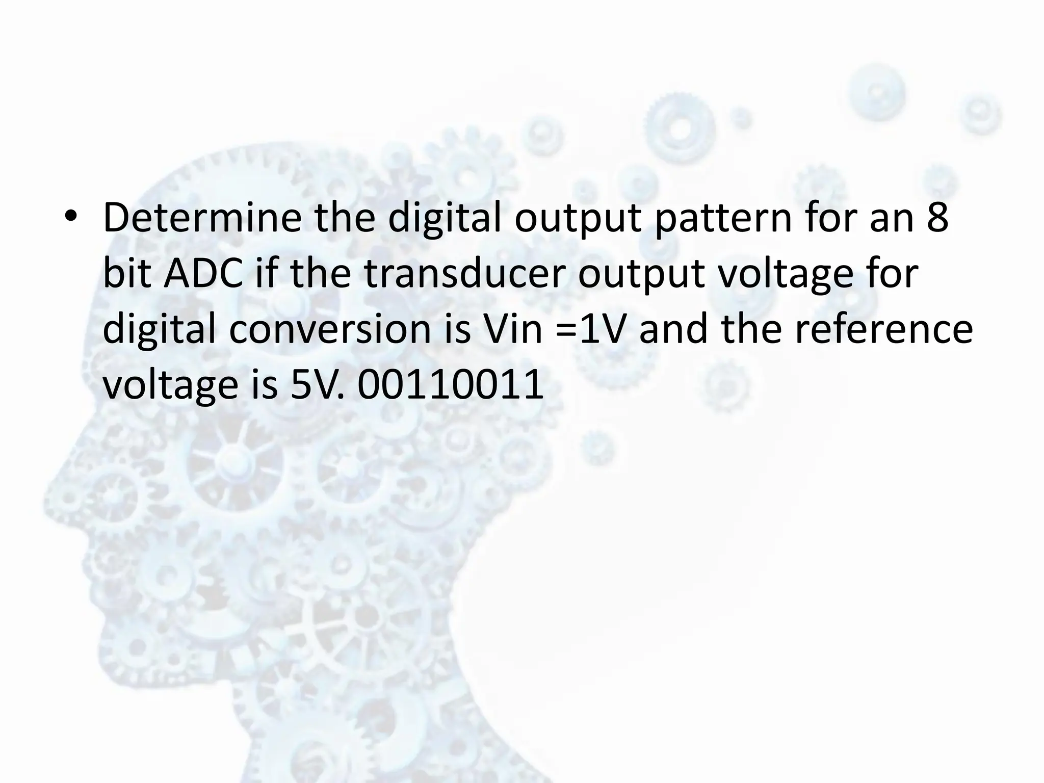
• Determine thedigital output pattern for an 8
bit ADC if the transducer output voltage for
digital conversion is Vin =1V and the reference
voltage is 5V. 00110011


![𝐴 = 𝜋𝑟2
Vo=[b5
1
𝑅
+b4
1
2𝑅
+..b0
1
32𝑅
] Rf*Vref](https://image.slidesharecdn.com/pdfunit-3signalconditioning-250324125010-b88a7774/75/PDF-UNIT-3-Signal-Coe2e3e3nditioning-pdf-45-2048.jpg)