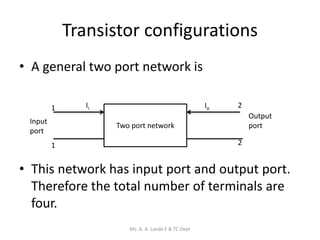
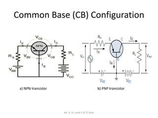
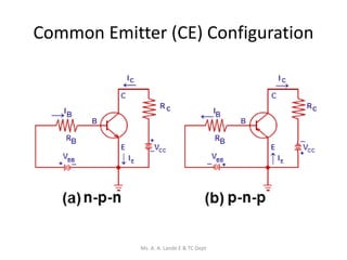
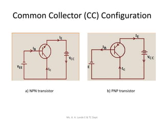
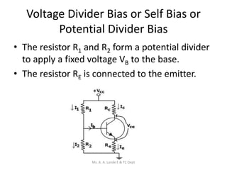
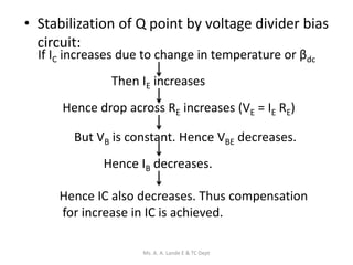
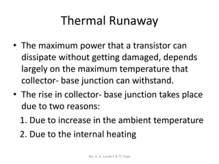
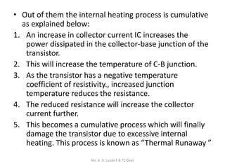
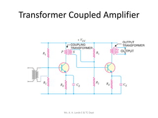
This document discusses transistor configurations and biasing. It describes the common base, common emitter, and common collector configurations. It explains how biasing circuits like fixed bias, collector feedback bias, and voltage divider bias can stabilize the operating point. Thermal runaway and the use of heat sinks are also covered. Single-stage amplifiers using common emitter configuration with input and output coupling capacitors are discussed. Finally, the concepts of frequency response and bandwidth are introduced.

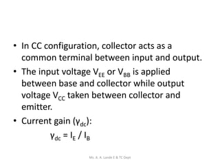
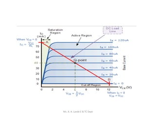
![• Apply KVL to collector circuit to write,
VCC – VCE – IC RC = 0 -----(1)
• Rearranging this equation we get,
IC = [-1 / RC] VCE + VCC/RC ------(2)
• Compare this equation with the general equation of a
straight line,
y = mx + C ------(3)
• From eq. (2) and (3), we get
y = IC x = VCE
m = -1/ RC C = VCC / RC
• This shows that eq. (2) represents a straight line. This
straight line is called as the dc load line.
Ms. A. A. Lande E & TC Dept](https://image.slidesharecdn.com/chapter2bem-240102092548-21aa878a/85/Transistor-cb-cc-ce-power-point-transistor-14-320.jpg)
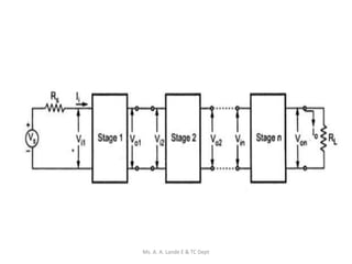
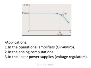
![• Overall output resistance (Ro):
The overall output resistance of a cascaded
amplifier is equal to the output resistance of the last
stage.
• Gain in decibels:
The gain expressed as a ratio of output voltage and
input voltage is called as the linear gain.
On the logarithmic scale the gain is expressed in
decibels as follows:
1. Power gain in dB = 10 log10 [Po/ Pi]
2. Voltage gain in dB = 20 log10 [Vo/ Vi]
Ms. A. A. Lande E & TC Dept](https://image.slidesharecdn.com/chapter2bem-240102092548-21aa878a/85/Transistor-cb-cc-ce-power-point-transistor-52-320.jpg)
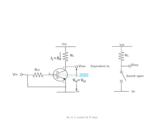
![Transistor as a Switch
• For switching applications, transistor is biased to
operate in the saturation (fully on) or cutoff (fully
off) regions.
1. Transistor in cutoff regions [open switch]:
In cutoff region, both junctions are reverse
biased and very small reverse current flows
through transistor.
Voltage drop across transistor (VCE)is high. Thus
transistor is equivalent to an open switch.
Ms. A. A. Lande E & TC Dept](https://image.slidesharecdn.com/chapter2bem-240102092548-21aa878a/85/Transistor-cb-cc-ce-power-point-transistor-61-320.jpg)
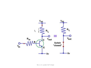
![2. Transistor in the saturation region [closed
switch]:
In saturation region, both junctions are
forward biased. The voltage drop across the
transistor is very small and collector current is
very large.
Thus in this region, transistor equivalent to a
closed switch.
Ms. A. A. Lande E & TC Dept](https://image.slidesharecdn.com/chapter2bem-240102092548-21aa878a/85/Transistor-cb-cc-ce-power-point-transistor-63-320.jpg)