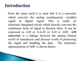
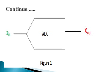
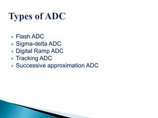
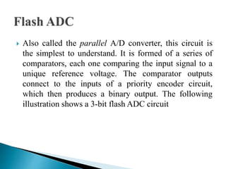
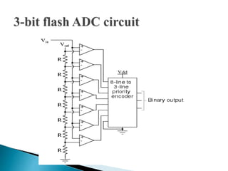
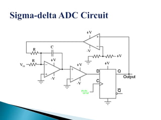
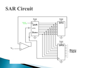
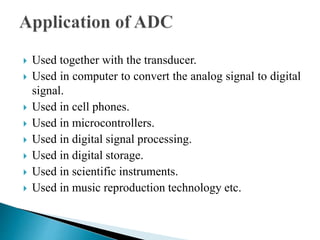
BY
ASHVANI KUMAR SHUKLA
M.E.(I&C)-2015
R.No-151503
Introduction
Type of ADC
 Flash ADC
 Sigma-delta ADC
 Digital Ramp ADC
 Tracking ADC
 Successive approximation
Application Of ADC
From the name itself it is clear that it is a converter
which converts the analog (continuously variable)
signal to digital signal. This is really an
electronic integrated circuit which directly converts the
continuous form of signal to discrete form. It can be
expressed as A/D or A-to-D or A-D or ADC. A/D
converter is a linkage between the analog (linear)
world of transducers and discreet world of processing
the signal and handling the data. The schematic
representation of ADC is shown below.
 Flash ADC
 Sigma-delta ADC
 Digital Ramp ADC
 Tracking ADC
 Successive approximation ADC
 Also called the parallel A/D converter, this circuit is
the simplest to understand. It is formed of a series of
comparators, each one comparing the input signal to a
unique reference voltage. The comparator outputs
connect to the inputs of a priority encoder circuit,
which then produces a binary output. The following
illustration shows a 3-bit flash ADC circuit
 In a ΔΣ converter, the analog input voltage signal is
connected to the input of an integrator, producing a
voltage rate-of-change, or slope, at the output
corresponding to input magnitude. This ramping
voltage is then compared against ground potential (0
volts) by a comparator. The comparator acts as a sort of
1-bit ADC, producing 1 bit of output (“high” or “low”)
depending on whether the integrator output is positive
or negative. The comparator’s output is then latched
through a D-type flip-flop clocked at a high frequency,
and fed back to another input channel on the integrator,
to drive the integrator in the direction of a 0 volt output.
The basic circuit looks like this.
The leftmost op-amp is the (summing) integrator. The
next op-amp the integrator feeds into is the comparator,
or 1-bit ADC. Next comes the D-type flip-flop, which
latches the comparator’s output at every clock pulse,
sending either a “high” or “low” signal to the next
comparator at the top of the circuit. This final
comparator is necessary to convert the single-polarity
0V / 5V logic level output voltage of the flip-flop into a
+V / -V voltage signal to be fed back to the integrator.
 If the integrator output is positive, the first comparator
will output a “high” signal to the D input of the flip-
flop. At the next clock pulse, this “high” signal will be
output from the Q line into the non inverting input of
the last comparator. This last comparator, seeing an
input voltage greater than the threshold voltage of 1/2
+V, saturates in a positive direction, sending a full +V
signal to the other
 input of the integrator. This +V feedback signal tends to
drive the integrator output in a negative direction. If
that output voltage ever becomes negative, the
feedback loop will send a corrective signal (-V) back
around to the top input of the integrator to drive it in a
positive direction. This is the delta-sigma concept in
action: the first comparator senses a difference (Δ)
between the integrator output and zero volts. The
integrator sums (Σ) the comparator’s output with the
analog input signal.
 Functionally, this results in a serial stream of bits
output by the flip-flop. If the analog input is zero volts,
the integrator will have no tendency to ramp either
positive or negative, except in response to the feedback
voltage. In this scenario, the flip-flop output will
continually oscillate between “high” and “low,” as the
feedback system “hunts” back and forth, trying to
maintain the integrator output at zero volts
 Also known as the stairstep-ramp, or
simply counter A/D converter, this is also fairly easy to
understand but unfortunately suffers from several
limitations.
 The basic idea is to connect the output of a free-running
binary counter to the input of a DAC, then compare the
analog output of the DAC with the analog input signal
to be digitized and use the comparator’s output to tell
the counter when to stop counting and reset. The
following schematic shows the basic idea
 As the counter counts up with each clock pulse, the DAC
outputs a slightly higher (more positive) voltage. This voltage
is compared against the input voltage by the comparator. If the
input voltage is greater than the DAC output, the comparator’s
output will be high and the counter will continue counting
normally. Eventually, though, the DAC output will exceed the
input voltage, causing the comparator’s output to go low. This
will cause two things to happen: first, the high-to-low
transition of the comparator’s output will cause the shift
register to “load” whatever binary count is being output by the
counter, thus updating the ADC circuit’s output; secondly, the
counter will receive a low signal on the active-low LOAD
input, causing it to reset to 00000000 on the next clock pulse.
 In tracking ADC,Instead of a regular “up” counter driving
the DAC, this circuit uses an up/down counter. The counter
is continuously clocked, and the up/down control line is
driven by the output of the comparator. So, when the analog
input signal exceeds the DAC output, the counter goes into
the “count up” mode. When the DAC output exceeds the
analog input, the counter switches into the “count down”
mode. Either way, the DAC output always counts in the
proper direction to track the input signal.
 Notice how no shift register is needed to buffer the binary
count at the end of a cycle. Since the counter’s output
continuously tracks the input (rather than counting to meet
the input and then resetting back to zero), the binary output
is legitimately updated with every clock pulse.
 An advantage of this converter circuit is speed, since the
counter never has to reset.
 One method of addressing the digital ramp ADC’s
shortcomings is the so-called successive-approximation
ADC. The only change in this design is a very special
counter circuit known as a successive-approximation
register. Instead of counting up in binary sequence, this
register counts by trying all values of bits starting with
the most-significant bit and finishing at the least-
significant bit. Throughout the count process, the
register monitors the comparator’s output to see if the
binary count is less than or greater than the analog
signal input, adjusting the bit values accordingly
 The way the register counts is identical to the “trial-
and-fit” method of decimal-to-binary conversion,
whereby different values of bits are tried from MSB to
LSB to get a binary number that equals the original
decimal number. The advantage to this counting
strategy is much faster results: the DAC output
converges on the analog signal input in much larger
steps than with the 0-to-full count sequence of a regular
counter.
 Without showing the inner workings of the successive-
approximation register (SAR), the circuit looks like this
 Used together with the transducer.
 Used in computer to convert the analog signal to digital
signal.
 Used in cell phones.
 Used in microcontrollers.
 Used in digital signal processing.
 Used in digital storage.
 Used in scientific instruments.
 Used in music reproduction technology etc.
THANK YOU..................

Adc.pptx ashvani 151503

  • 1.
  • 2.
    Introduction Type of ADC Flash ADC  Sigma-delta ADC  Digital Ramp ADC  Tracking ADC  Successive approximation Application Of ADC
  • 3.
    From the nameitself it is clear that it is a converter which converts the analog (continuously variable) signal to digital signal. This is really an electronic integrated circuit which directly converts the continuous form of signal to discrete form. It can be expressed as A/D or A-to-D or A-D or ADC. A/D converter is a linkage between the analog (linear) world of transducers and discreet world of processing the signal and handling the data. The schematic representation of ADC is shown below.
  • 5.
     Flash ADC Sigma-delta ADC  Digital Ramp ADC  Tracking ADC  Successive approximation ADC
  • 6.
     Also calledthe parallel A/D converter, this circuit is the simplest to understand. It is formed of a series of comparators, each one comparing the input signal to a unique reference voltage. The comparator outputs connect to the inputs of a priority encoder circuit, which then produces a binary output. The following illustration shows a 3-bit flash ADC circuit
  • 8.
     In aΔΣ converter, the analog input voltage signal is connected to the input of an integrator, producing a voltage rate-of-change, or slope, at the output corresponding to input magnitude. This ramping voltage is then compared against ground potential (0 volts) by a comparator. The comparator acts as a sort of 1-bit ADC, producing 1 bit of output (“high” or “low”) depending on whether the integrator output is positive or negative. The comparator’s output is then latched through a D-type flip-flop clocked at a high frequency, and fed back to another input channel on the integrator, to drive the integrator in the direction of a 0 volt output. The basic circuit looks like this.
  • 10.
    The leftmost op-ampis the (summing) integrator. The next op-amp the integrator feeds into is the comparator, or 1-bit ADC. Next comes the D-type flip-flop, which latches the comparator’s output at every clock pulse, sending either a “high” or “low” signal to the next comparator at the top of the circuit. This final comparator is necessary to convert the single-polarity 0V / 5V logic level output voltage of the flip-flop into a +V / -V voltage signal to be fed back to the integrator.
  • 11.
     If theintegrator output is positive, the first comparator will output a “high” signal to the D input of the flip- flop. At the next clock pulse, this “high” signal will be output from the Q line into the non inverting input of the last comparator. This last comparator, seeing an input voltage greater than the threshold voltage of 1/2 +V, saturates in a positive direction, sending a full +V signal to the other
  • 12.
     input ofthe integrator. This +V feedback signal tends to drive the integrator output in a negative direction. If that output voltage ever becomes negative, the feedback loop will send a corrective signal (-V) back around to the top input of the integrator to drive it in a positive direction. This is the delta-sigma concept in action: the first comparator senses a difference (Δ) between the integrator output and zero volts. The integrator sums (Σ) the comparator’s output with the analog input signal.
  • 13.
     Functionally, thisresults in a serial stream of bits output by the flip-flop. If the analog input is zero volts, the integrator will have no tendency to ramp either positive or negative, except in response to the feedback voltage. In this scenario, the flip-flop output will continually oscillate between “high” and “low,” as the feedback system “hunts” back and forth, trying to maintain the integrator output at zero volts
  • 15.
     Also knownas the stairstep-ramp, or simply counter A/D converter, this is also fairly easy to understand but unfortunately suffers from several limitations.  The basic idea is to connect the output of a free-running binary counter to the input of a DAC, then compare the analog output of the DAC with the analog input signal to be digitized and use the comparator’s output to tell the counter when to stop counting and reset. The following schematic shows the basic idea
  • 17.
     As thecounter counts up with each clock pulse, the DAC outputs a slightly higher (more positive) voltage. This voltage is compared against the input voltage by the comparator. If the input voltage is greater than the DAC output, the comparator’s output will be high and the counter will continue counting normally. Eventually, though, the DAC output will exceed the input voltage, causing the comparator’s output to go low. This will cause two things to happen: first, the high-to-low transition of the comparator’s output will cause the shift register to “load” whatever binary count is being output by the counter, thus updating the ADC circuit’s output; secondly, the counter will receive a low signal on the active-low LOAD input, causing it to reset to 00000000 on the next clock pulse.
  • 18.
     In trackingADC,Instead of a regular “up” counter driving the DAC, this circuit uses an up/down counter. The counter is continuously clocked, and the up/down control line is driven by the output of the comparator. So, when the analog input signal exceeds the DAC output, the counter goes into the “count up” mode. When the DAC output exceeds the analog input, the counter switches into the “count down” mode. Either way, the DAC output always counts in the proper direction to track the input signal.  Notice how no shift register is needed to buffer the binary count at the end of a cycle. Since the counter’s output continuously tracks the input (rather than counting to meet the input and then resetting back to zero), the binary output is legitimately updated with every clock pulse.  An advantage of this converter circuit is speed, since the counter never has to reset.
  • 20.
     One methodof addressing the digital ramp ADC’s shortcomings is the so-called successive-approximation ADC. The only change in this design is a very special counter circuit known as a successive-approximation register. Instead of counting up in binary sequence, this register counts by trying all values of bits starting with the most-significant bit and finishing at the least- significant bit. Throughout the count process, the register monitors the comparator’s output to see if the binary count is less than or greater than the analog signal input, adjusting the bit values accordingly
  • 21.
     The waythe register counts is identical to the “trial- and-fit” method of decimal-to-binary conversion, whereby different values of bits are tried from MSB to LSB to get a binary number that equals the original decimal number. The advantage to this counting strategy is much faster results: the DAC output converges on the analog signal input in much larger steps than with the 0-to-full count sequence of a regular counter.  Without showing the inner workings of the successive- approximation register (SAR), the circuit looks like this
  • 23.
     Used togetherwith the transducer.  Used in computer to convert the analog signal to digital signal.  Used in cell phones.  Used in microcontrollers.  Used in digital signal processing.  Used in digital storage.  Used in scientific instruments.  Used in music reproduction technology etc.
  • 24.