TataKelola dan KamSiber Kecerdasan Buatan v022.pdf
analog to digital adn digital to analog .ppt
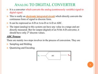
1. ANALOG TO DIGITAL CONVERTER
It is a converter which converts the analog (continuously variable) signal to
digital signal.
This is really an electronic integrated circuit which directly converts the
continuous form of signal to discrete form.
It can be expressed as A/D or A-to-D or A-D or ADC.
The input (analog) to this system can have any value in a range and are
directly measured. But for output (digital) of an N-bit A/D converter, it
should have only 2N discrete values.
ADC Process
There are mainly two steps involves in the process of conversion. They are
Sampling and Holding
Quantizing and Encoding
1
2. Sampling and Holding
In the process of Sample and hold (S/H), the continuous signal will gets sampled and
freeze (hold) the value at a steady level for a particular least period of time.
It is done to remove variations in input signal which can increases the accuracy.
Quantizing and Encoding
It is the smallest variation in analog signal that will result in a variation in the digital output. This
actually represents the quantization error.
V → Reference voltage range
2N → Number of states
N → Number of bits in digital output
2
The whole ADC conversion process
3. Types of Analog to Digital Converter
Successive Approximation ADC: This converter compares the input signal with the
output of an internal DAC at each successive step. It is the most expensive type.
Dual Slope ADC: It have high accuracy but very slow in operation.
Pipeline ADC: It is same as that of two step Flash ADC.
Delta-Sigma ADC: It has high resolution but slow due to over sampling.
Flash ADC: It is the fastest ADC but very expensive.
Other: Staircase ramp, Voltage-to-Frequency, Switched capacitor, tracking, Charge
balancing, and resolver.
Successive Approximation ADC
A successive approximation type ADC produces a digital output, which is
approximately equal to the analog input by using successive approximation technique
internally.
The block diagram of a successive approximation ADC
3
4. The successive approximation ADC mainly consists of 5 blocks− Clock signal generator,
Successive Approximation Register (SAR), DAC, comparator and Control logic.
The working of a successive approximation ADC is as follows −
The control logic resets all the bits of SAR and enables the clock signal generator in order to send
the clock pulses to SAR, when it received the start commanding signal.
The binary (digital) data present in SAR will be updated for every clock pulse based on the output
of comparator. The output of SAR is applied as an input of DAC.
DAC converts the received digital input, which is the output of SAR, into an analog output. The
comparator compares this analog value Va with the external analog input value Vi.
The output of a comparator will be ‘1’ as long as Vi is greater than Va. Similarly, the output of
comparator will be ‘0’, when Vi is less than or equal to Va.
The operations mentioned in above steps will be continued until the digital output is a valid one.
The digital output will be a valid one, when it is almost equivalent to the corresponding external
analog input value Vi.
4
5. Flash type ADC
A flash type ADC produces an equivalent digital output for a corresponding analog input in no time. Hence, flash
type ADC is the fastest ADC.
The circuit diagram of a 3-bit flash type ADC is
5
6. The 3-bit flash type ADC consists of a voltage divider network, 7 comparators and a
priority encoder.
The working of a 3-bit flash type ADC is as follows.
The voltage divider network contains 8 equal resistors. A reference voltage VR is
applied across that entire network with respect to the ground. The voltage drop across
each resistor from bottom to top with respect to ground will be the integer multiples
(from 1 to 8) of VR8.
The external input voltage Vi is applied to the non-inverting terminal of all
comparators. The voltage drop across each resistor from bottom to top with respect to
ground is applied to the inverting terminal of comparators from bottom to top.
At a time, all the comparators compare the external input voltage with the voltage
drops present at the respective other input terminal. That means, the comparison
operations take place by each comparator parallels.
The output of the comparator will be ‘1’ as long as Vi is greater than the voltage
drop present at the respective other input terminal. Similarly, the output of
comparator will be ‘0’, when, Vi is less than or equal to the voltage drop present at
the respective other input terminal.
All the outputs of comparators are connected as the inputs of priority encoder.This
priority encoder produces a binary code (digital output), which is corresponding to
the high priority input that has ‘1’.
Therefore, the output of priority encoder is nothing but the binary equivalent (digital
output) of external analog input voltage, Vi
6
7. Application of ADC
Used together with the transducer.
Used in computer to convert the analog signal to digital
signal.
Used in cell phones.
Used in microcontrollers.
Used in digital signal processing.
Used in digital storage oscilloscopes.
Used in scientific instruments.
Used in music reproduction technology etc.
7
8. DIGITAL TO ANALOG CONVERTER
A Digital to Analog Converter (DAC) converts a digital input signal into
an analog output signal. The digital signal is represented with a binary code,
which is a combination of bits 0 and 1.
Op amp is extensively used as main building block of digital to analog
convertor. Digital to analog convertor is an electronics device in form of
IC.
A Digital to Analog Converter (DAC) consists of a number of binary inputs and a
single output. In general, the number of binary inputs of a DAC will be a power of
two.
Types of DACs
There are two types of DACs
Weighted Resistor DAC
R-2R Ladder DAC
8
9. WEIGHTED RESISTOR DAC
A weighted resistor DAC produces an analog output, which is almost equal
to the digital (binary) input by using binary weighted resistors in the
inverting adder circuit. In short, a binary weighted resistor DAC is called as
weighted resistor DAC.
9
10. Let the 3-bit binary input is b2,b1&b0.
Here, the bits b2 and b0 denote the Most Significant Bit (MSB) and Least
Significant Bit (LSB) respectively.
The digital switches will be connected to ground, when the corresponding
input bits are equal to ‘0’.
Similarly, the digital switches will be connected to the negative reference
voltage, −VR when the corresponding input bits are equal to ‘1’.
In the above circuit, the non-inverting input terminal of an op-amp is
connected to ground. That means zero volts is applied at the non-inverting
input terminal of op-amp.
According to the virtual short concept, the voltage at the inverting input
terminal of op-amp is same as that of the voltage present at its non-inverting
input terminal. So, the voltage at the inverting input terminal’s node will be
zero volts.
10
11. 11
The nodal equation at the inverting input terminal’s node is:
The above equation represents the output voltage equation of a 3-bit binary weighted resistor DAC.
We can write the generalized output voltage equation
The disadvantages of a binary weighted resistor DAC are as follows −
The difference between the resistance values corresponding to LSB & MSB will increase as the number of bits present
in the digital input increases.
It is difficult to design more accurate resistors as the number of bits present in the digital input increases.
12. R-2R LADDER DAC
The R-2R Ladder DAC overcomes the disadvantages of a binary weighted
resistor DAC. As the name suggests, R-2R Ladder DAC produces an analog
output, which is almost equal to the digital (binary) input by using a R-2R
ladder network in the inverting adder circuit.
12
13. R-2R Ladder
This is the simplest type of DAC and needs only two resistor values
arranged in a ladder. You can think of this as a somewhat complex voltage
divider, though the math is quite complex.
The binary input goes into the 2R resistors and the output is obtained at the
bottom of the ladder.
Applications of DACs
1. Digital Signal Processing
2. Digital Power Supplies
Drawbacks of DACS
1. Accuracy
2. Complexity
13