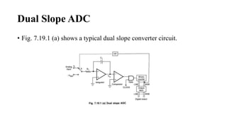
Dual Slope ADC
Dr.R.Hepzi Pramila Devamani,
Assistant Professor of Physics,
V.V.Vanniaperumal College for Women,
Virudhunagar.
Dual Slope ADC
• Dual slope conversion is an indirect method for A/D conversion where
an analog voltage and a reference voltage are converted into time
periods by an integrator and then measured by a counter.
• The speed of this conversion is slow but the accuracy is high.
Dual Slope ADC
• Fig. 7.19.1 (a) shows a typical dual slope converter circuit.
Dual Slope ADC
• It consists of integrator (ramp generator), comparator, binary counter,
output latch and reference voltage.
• The ramp generator input is switched between the analog input voltage
Vi and a negative reference voltage, -VREF.
• The analog switch is controlled by the MSB of the counter.
Dual Slope ADC
• When the MSB is a logic 0, the voltage being measured is connected
to the ramp generator input.
• When MSB is logic 1, the negative reference voltage is connected to
the ramp generator.
• At time t = 0, analog switch S is connected to the analog input voltage
integration begins.
• The output voltage of the integrator can be given as
Dual Slope ADC
• where R1 C1 is the integrator time constant and V, is assumed constant
over the integration time period.
• At the end of 2N clock periods MSB of the counter goes high.
• At a result the output of the flip-flop goes high, which causes analog
switch S to be switched from Vi to -Vg.
• At this very same time the binary counter which has gone through its
entire count sequence is reset.
Dual Slope ADC
• The negative input voltage (-Vg) connected to the input of integrator
causes the integrator output to ramp positive.
• When integrator output reaches zero, the comparator output voltage
goes low, which disables the clock AND gate.
• This stops the clock reaching the counter, so that the counter will be
stopped at a count corresponding number of clock pulses in time t2
Dual Slope ADC
• The integrator output ramp down to a voltage V and get back upto o.
• Therefore, the charge voltage is equal to discharge voltage and we can
write
Dual Slope ADC
• The above equation shows that t2 is directly proportional only to the Vi, since VR
and t1 are constants.
• The binary digital output of the counter gives corresponding digital value for time
period t2 and hence it is also directly proportional to input signal Vi.
• The actual conversion of analog voltage Vi into a digital count occurs during t2 .
• The control circuit connects the clock to the counter at the beginning of t2.
• The clock is disconnected at the end of t2.
• Thus the counter contents is digital output.
• Hence we can write
Dual Slope ADC
The counter output can then be connected to an appropriate digital
display.
The advantages of dual slope ADC are
• It is highly accurate.
• Its cost is low.
• It is immune to temperature caused variations in R1 and C₁.
The only disadvantage of this ADC is its speed which is low.
THANK YOU

Dual Slope ADC.pptx

  • 1.
    Dual Slope ADC Dr.R.HepziPramila Devamani, Assistant Professor of Physics, V.V.Vanniaperumal College for Women, Virudhunagar.
  • 2.
    Dual Slope ADC •Dual slope conversion is an indirect method for A/D conversion where an analog voltage and a reference voltage are converted into time periods by an integrator and then measured by a counter. • The speed of this conversion is slow but the accuracy is high.
  • 3.
    Dual Slope ADC •Fig. 7.19.1 (a) shows a typical dual slope converter circuit.
  • 4.
    Dual Slope ADC •It consists of integrator (ramp generator), comparator, binary counter, output latch and reference voltage. • The ramp generator input is switched between the analog input voltage Vi and a negative reference voltage, -VREF. • The analog switch is controlled by the MSB of the counter.
  • 5.
    Dual Slope ADC •When the MSB is a logic 0, the voltage being measured is connected to the ramp generator input. • When MSB is logic 1, the negative reference voltage is connected to the ramp generator. • At time t = 0, analog switch S is connected to the analog input voltage integration begins. • The output voltage of the integrator can be given as
  • 6.
    Dual Slope ADC •where R1 C1 is the integrator time constant and V, is assumed constant over the integration time period. • At the end of 2N clock periods MSB of the counter goes high. • At a result the output of the flip-flop goes high, which causes analog switch S to be switched from Vi to -Vg. • At this very same time the binary counter which has gone through its entire count sequence is reset.
  • 7.
    Dual Slope ADC •The negative input voltage (-Vg) connected to the input of integrator causes the integrator output to ramp positive. • When integrator output reaches zero, the comparator output voltage goes low, which disables the clock AND gate. • This stops the clock reaching the counter, so that the counter will be stopped at a count corresponding number of clock pulses in time t2
  • 8.
    Dual Slope ADC •The integrator output ramp down to a voltage V and get back upto o. • Therefore, the charge voltage is equal to discharge voltage and we can write
  • 9.
    Dual Slope ADC •The above equation shows that t2 is directly proportional only to the Vi, since VR and t1 are constants. • The binary digital output of the counter gives corresponding digital value for time period t2 and hence it is also directly proportional to input signal Vi. • The actual conversion of analog voltage Vi into a digital count occurs during t2 . • The control circuit connects the clock to the counter at the beginning of t2. • The clock is disconnected at the end of t2. • Thus the counter contents is digital output. • Hence we can write
  • 10.
    Dual Slope ADC Thecounter output can then be connected to an appropriate digital display. The advantages of dual slope ADC are • It is highly accurate. • Its cost is low. • It is immune to temperature caused variations in R1 and C₁. The only disadvantage of this ADC is its speed which is low.
  • 11.