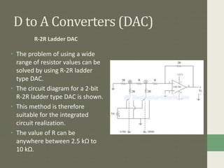
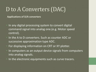
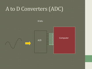
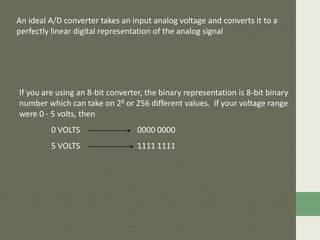
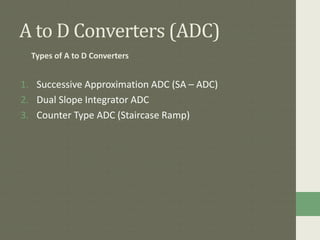
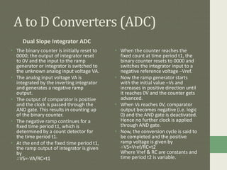
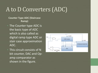
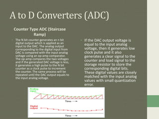
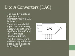
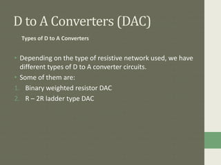
Data Converters
Digital to Analog Converters (DACs)
Analog to Digital Converters (ADCs)
Sine
Wave
Random-
Periodic
Analog :-
An analog signal is a continuous signal that contains time-
varying quantities, such as temperature or speed, with infinite
possible values in between
An analog signal can be used to measure changes in some
physical phenomena such as light, sound, pressure, or
temperature.
Digital -:
A Digital signal is a type of signal that can take on a set
of discrete values (a quantized signal)
Digital signals can represent a discrete set of values using any
discrete set of waveforms .. And we can represent it like (0 or
1) ,( on or off )….. etc
Example:
A digital thermostat in a
room displays a temperature
of 72. An analog
thermometer measures the
room temperature at
72.482. The analog value is
continuous and more
accurate, but the digital
value is more than adequate
for the application and
significantly easier to process
electronically.
Digital Signals
 Discrete
 Finite range of values
 Not as exact as analog,
but easier to work with
Analog Signals
 Continuous
 Infinite range of values
 More exact values, but
more difficult to work
with
D to A Converters (DAC)
• The circuit symbol and
input-output
characteristics of a DAC
is shown.
• There are four digital
inputs and one analog
output. “d0” is the most
significant bit MSB and
“d3” is the least
significant bit LSB.
• The 3-bit digital word
will have eight different
possible combinations
from 000 to 111.
D to A Converters (DAC)
Input – Output Equation
• If the input to a DAC block is an “n” bit
digital word and analog output voltage
V0 then the expression for the analog
output voltage V0 is given by,
• V0 = VFS [d1 2-1 + d2 2-2 + … + dn 2-n ]
• We can substitute VFS by VR .i.e. the
reference voltage to write
• V0 = KVR [d1 2-1 + d2 2-2 + … + dn 2-n ]
• If we substitute ,
D = [d1 2-1 + d2 2-2 + … + dn 2-n ] then
V0 = K VR D
• The input and output equation is
applicable to all types of DACs.
• Where,
 VFS = Full Scale
output voltage.
d1 = MSB
dn = LSB
K = scaling factor
D = fractional binary
value
D to A Converters (DAC)
Types of D to A Converters
• Depending on the type of resistive network used, we have
different types of D to A converter circuits.
• Some of them are:
1. Binary weighted resistor DAC
2. R – 2R ladder type DAC
D to A Converters (DAC)
Binary Weighted Resistor DAC
• This DAC circuit uses weighted values
of resistor like 2R, 4R, 6R, 8R and so on
depending on the digital inputs
available therefore such type of
network is known as weighted resistor
DAC.
• This circuit consists of a transistor
switch which turns on the switch when
the digital input is ‘1’ and if digital input
becomes ‘0’ it will open the switch.
When transistor switch gets closed,
current flows through the weighted
resistor due to the reference voltage.
• When all such currents from different
weighted resistors get added at
summing point of the operational
amplifier it will produce a proportional
voltage as its output.
• V0 = VR [d1 2-1 + d2 2-2 + ….. + dn 2-n ]
D to A Converters (DAC)
R-2R Ladder DAC
• The problem of using a wide
range of resistor values can be
solved by using R-2R ladder
type DAC.
• The circuit diagram for a 2-bit
R-2R ladder type DAC is shown.
• This method is therefore
suitable for the integrated
circuit realization.
• The value of R can be
anywhere between 2.5 kΩ to
10 kΩ.
D to A Converters (DAC)
Applications of D/A converters
• In any digital processing system to convert digital
command signal into analog one.(e.g. Motor speed
control).
• In the A to D converters. Such as counter ADC or
successive approximation type ADC.
• For displaying information on CRT or XY plotter.
• In computers as an output device signals from computers
into analog signals.
• In the electronic equipments such as curve tracers.
A/D
8 bits
Computer
A to D Converters (ADC)
An ideal A/D converter takes an input analog voltage and converts it to a
perfectly linear digital representation of the analog signal
If you are using an 8-bit converter, the binary representation is 8-bit binary
number which can take on 28 or 256 different values. If your voltage range
were 0 - 5 volts, then
0 VOLTS 0000 0000
5 VOLTS 1111 1111
A to D Converters (ADC)
Types of A to D Converters
1. Successive Approximation ADC (SA – ADC)
2. Dual Slope Integrator ADC
3. Counter Type ADC (Staircase Ramp)
A to D Converters (ADC)
Successive Approximation ADC
(SA – ADC)
• A successive approximation ADC is a type
of A/D converter that converts a continuous
analog waveform into a discrete digital
representation via a binary search through
all possible quantization levels before finally
converging upon a digital output for each
conversion.
• The successive approximation register is
initialized so that the most significant
bit (MSB) is equal to a digital 1. This code is
fed into the DAC, which then supplies the
analog equivalent of this digital code into
the comparator circuit for comparison with
the sampled input voltage.
• If this analog voltage exceeds Vin the
comparator causes the SAR to reset this bit;
otherwise, the bit is left a 1. Then the next
bit is set to 1 and the same test is done,
continuing this binary search until every bit
in the SAR has been tested.
A to D Converters (ADC)
Successive Approximation ADC
(SA – ADC)
A to D Converters (ADC)
Dual Slope Integrator ADC
• In dual slope type ADC, the
integrator generates two
different ramps, one with the
known analog input voltage VA
and another with a known
reference voltage –Vref.
• Hence it is called a s dual slope
A to D converter.
A to D Converters (ADC)
Dual Slope Integrator ADC
• The binary counter is initially reset to
0000; the output of integrator reset
to 0V and the input to the ramp
generator or integrator is switched to
the unknown analog input voltage VA.
• The analog input voltage VA is
integrated by the inverting integrator
and generates a negative ramp
output.
• The output of comparator is positive
and the clock is passed through the
AND gate. This results in counting up
of the binary counter.
• The negative ramp continues for a
fixed time period t1, which is
determined by a count detector for
the time period t1.
• At the end of the fixed time period t1,
the ramp output of integrator is given
by
∴VS=-VA/RC×t1
• When the counter reaches the
fixed count at time period t1, the
binary counter resets to 0000 and
switches the integrator input to a
negative reference voltage –Vref.
• Now the ramp generator starts
with the initial value –Vs and
increases in positive direction until
it reaches 0V and the counter gets
advanced.
• When Vs reaches 0V, comparator
output becomes negative (i.e. logic
0) and the AND gate is deactivated.
Hence no further clock is applied
through AND gate.
• Now, the conversion cycle is said to
be completed and the positive
ramp voltage is given by
∴VS=Vref/RC×t2
Where Vref & RC are constants and
time period t2 is variable.
A to D Converters (ADC)
Counter Type ADC (Staircase
Ramp)
• The Counter type ADC is
the basic type of ADC
which is also called as
digital ramp type ADC or
stair case approximation
ADC.
• This circuit consists of N
bit counter, DAC and Op-
amp comparator as
shown in the figure.
A to D Converters (ADC)
Counter Type ADC (Staircase
Ramp)
• The N bit counter generates an n bit
digital output which is applied as an
input to the DAC. The analog output
corresponding to the digital input from
DAC is compared with the input analog
voltage using an op-amp comparator.
The op-amp compares the two voltages
and if the generated DAC voltage is less,
it generates a high pulse to the N bit
counter as a clock pulse to increment
the counter. The same process will be
repeated until the DAC output equals to
the input analog voltage.
• If the DAC output voltage is
equal to the input analog
voltage, then it generates low
clock pulse and it also
generates a clear signal to the
counter and load signal to the
storage resistor to store the
corresponding digital bits.
These digital values are closely
matched with the input analog
values with small quantization
error.
Data convertors

Data convertors

  • 1.
    Data Converters Digital toAnalog Converters (DACs) Analog to Digital Converters (ADCs)
  • 2.
    Sine Wave Random- Periodic Analog :- An analogsignal is a continuous signal that contains time- varying quantities, such as temperature or speed, with infinite possible values in between An analog signal can be used to measure changes in some physical phenomena such as light, sound, pressure, or temperature.
  • 3.
    Digital -: A Digitalsignal is a type of signal that can take on a set of discrete values (a quantized signal) Digital signals can represent a discrete set of values using any discrete set of waveforms .. And we can represent it like (0 or 1) ,( on or off )….. etc
  • 4.
    Example: A digital thermostatin a room displays a temperature of 72. An analog thermometer measures the room temperature at 72.482. The analog value is continuous and more accurate, but the digital value is more than adequate for the application and significantly easier to process electronically. Digital Signals  Discrete  Finite range of values  Not as exact as analog, but easier to work with Analog Signals  Continuous  Infinite range of values  More exact values, but more difficult to work with
  • 5.
    D to AConverters (DAC) • The circuit symbol and input-output characteristics of a DAC is shown. • There are four digital inputs and one analog output. “d0” is the most significant bit MSB and “d3” is the least significant bit LSB. • The 3-bit digital word will have eight different possible combinations from 000 to 111.
  • 6.
    D to AConverters (DAC) Input – Output Equation • If the input to a DAC block is an “n” bit digital word and analog output voltage V0 then the expression for the analog output voltage V0 is given by, • V0 = VFS [d1 2-1 + d2 2-2 + … + dn 2-n ] • We can substitute VFS by VR .i.e. the reference voltage to write • V0 = KVR [d1 2-1 + d2 2-2 + … + dn 2-n ] • If we substitute , D = [d1 2-1 + d2 2-2 + … + dn 2-n ] then V0 = K VR D • The input and output equation is applicable to all types of DACs. • Where,  VFS = Full Scale output voltage. d1 = MSB dn = LSB K = scaling factor D = fractional binary value
  • 7.
    D to AConverters (DAC) Types of D to A Converters • Depending on the type of resistive network used, we have different types of D to A converter circuits. • Some of them are: 1. Binary weighted resistor DAC 2. R – 2R ladder type DAC
  • 8.
    D to AConverters (DAC) Binary Weighted Resistor DAC • This DAC circuit uses weighted values of resistor like 2R, 4R, 6R, 8R and so on depending on the digital inputs available therefore such type of network is known as weighted resistor DAC. • This circuit consists of a transistor switch which turns on the switch when the digital input is ‘1’ and if digital input becomes ‘0’ it will open the switch. When transistor switch gets closed, current flows through the weighted resistor due to the reference voltage. • When all such currents from different weighted resistors get added at summing point of the operational amplifier it will produce a proportional voltage as its output. • V0 = VR [d1 2-1 + d2 2-2 + ….. + dn 2-n ]
  • 9.
    D to AConverters (DAC) R-2R Ladder DAC • The problem of using a wide range of resistor values can be solved by using R-2R ladder type DAC. • The circuit diagram for a 2-bit R-2R ladder type DAC is shown. • This method is therefore suitable for the integrated circuit realization. • The value of R can be anywhere between 2.5 kΩ to 10 kΩ.
  • 10.
    D to AConverters (DAC) Applications of D/A converters • In any digital processing system to convert digital command signal into analog one.(e.g. Motor speed control). • In the A to D converters. Such as counter ADC or successive approximation type ADC. • For displaying information on CRT or XY plotter. • In computers as an output device signals from computers into analog signals. • In the electronic equipments such as curve tracers.
  • 11.
    A/D 8 bits Computer A toD Converters (ADC)
  • 12.
    An ideal A/Dconverter takes an input analog voltage and converts it to a perfectly linear digital representation of the analog signal If you are using an 8-bit converter, the binary representation is 8-bit binary number which can take on 28 or 256 different values. If your voltage range were 0 - 5 volts, then 0 VOLTS 0000 0000 5 VOLTS 1111 1111
  • 13.
    A to DConverters (ADC) Types of A to D Converters 1. Successive Approximation ADC (SA – ADC) 2. Dual Slope Integrator ADC 3. Counter Type ADC (Staircase Ramp)
  • 14.
    A to DConverters (ADC) Successive Approximation ADC (SA – ADC) • A successive approximation ADC is a type of A/D converter that converts a continuous analog waveform into a discrete digital representation via a binary search through all possible quantization levels before finally converging upon a digital output for each conversion. • The successive approximation register is initialized so that the most significant bit (MSB) is equal to a digital 1. This code is fed into the DAC, which then supplies the analog equivalent of this digital code into the comparator circuit for comparison with the sampled input voltage. • If this analog voltage exceeds Vin the comparator causes the SAR to reset this bit; otherwise, the bit is left a 1. Then the next bit is set to 1 and the same test is done, continuing this binary search until every bit in the SAR has been tested.
  • 15.
    A to DConverters (ADC) Successive Approximation ADC (SA – ADC)
  • 16.
    A to DConverters (ADC) Dual Slope Integrator ADC • In dual slope type ADC, the integrator generates two different ramps, one with the known analog input voltage VA and another with a known reference voltage –Vref. • Hence it is called a s dual slope A to D converter.
  • 17.
    A to DConverters (ADC) Dual Slope Integrator ADC • The binary counter is initially reset to 0000; the output of integrator reset to 0V and the input to the ramp generator or integrator is switched to the unknown analog input voltage VA. • The analog input voltage VA is integrated by the inverting integrator and generates a negative ramp output. • The output of comparator is positive and the clock is passed through the AND gate. This results in counting up of the binary counter. • The negative ramp continues for a fixed time period t1, which is determined by a count detector for the time period t1. • At the end of the fixed time period t1, the ramp output of integrator is given by ∴VS=-VA/RC×t1 • When the counter reaches the fixed count at time period t1, the binary counter resets to 0000 and switches the integrator input to a negative reference voltage –Vref. • Now the ramp generator starts with the initial value –Vs and increases in positive direction until it reaches 0V and the counter gets advanced. • When Vs reaches 0V, comparator output becomes negative (i.e. logic 0) and the AND gate is deactivated. Hence no further clock is applied through AND gate. • Now, the conversion cycle is said to be completed and the positive ramp voltage is given by ∴VS=Vref/RC×t2 Where Vref & RC are constants and time period t2 is variable.
  • 18.
    A to DConverters (ADC) Counter Type ADC (Staircase Ramp) • The Counter type ADC is the basic type of ADC which is also called as digital ramp type ADC or stair case approximation ADC. • This circuit consists of N bit counter, DAC and Op- amp comparator as shown in the figure.
  • 19.
    A to DConverters (ADC) Counter Type ADC (Staircase Ramp) • The N bit counter generates an n bit digital output which is applied as an input to the DAC. The analog output corresponding to the digital input from DAC is compared with the input analog voltage using an op-amp comparator. The op-amp compares the two voltages and if the generated DAC voltage is less, it generates a high pulse to the N bit counter as a clock pulse to increment the counter. The same process will be repeated until the DAC output equals to the input analog voltage. • If the DAC output voltage is equal to the input analog voltage, then it generates low clock pulse and it also generates a clear signal to the counter and load signal to the storage resistor to store the corresponding digital bits. These digital values are closely matched with the input analog values with small quantization error.