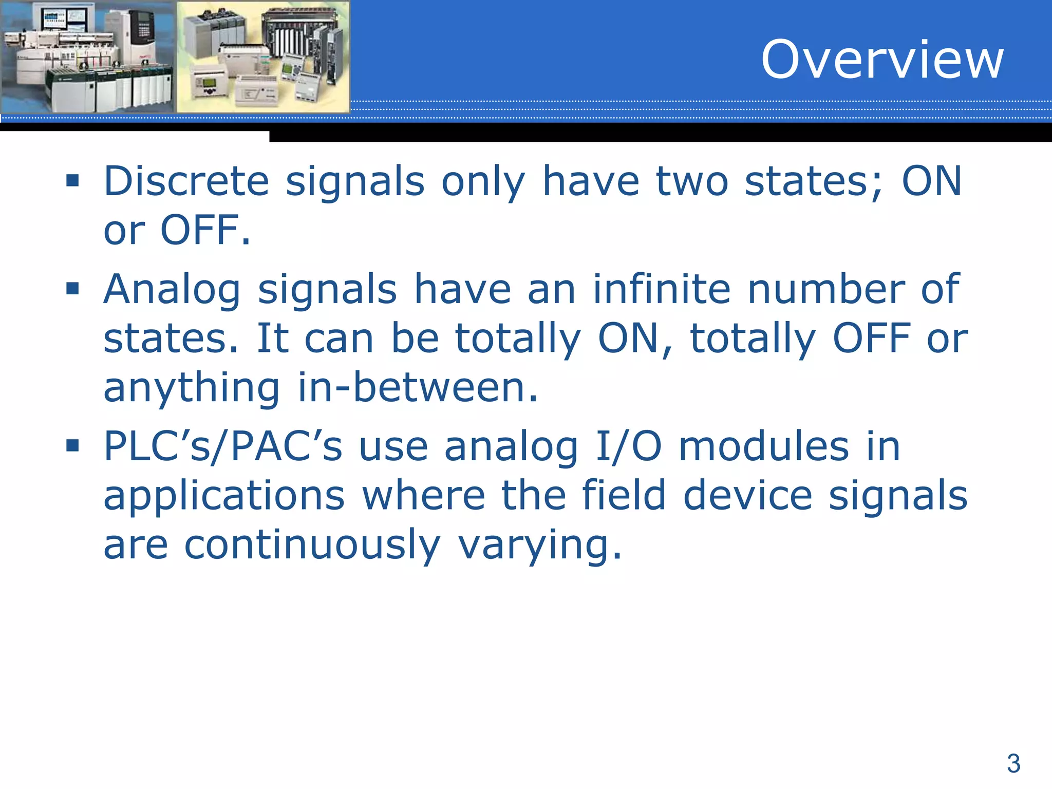
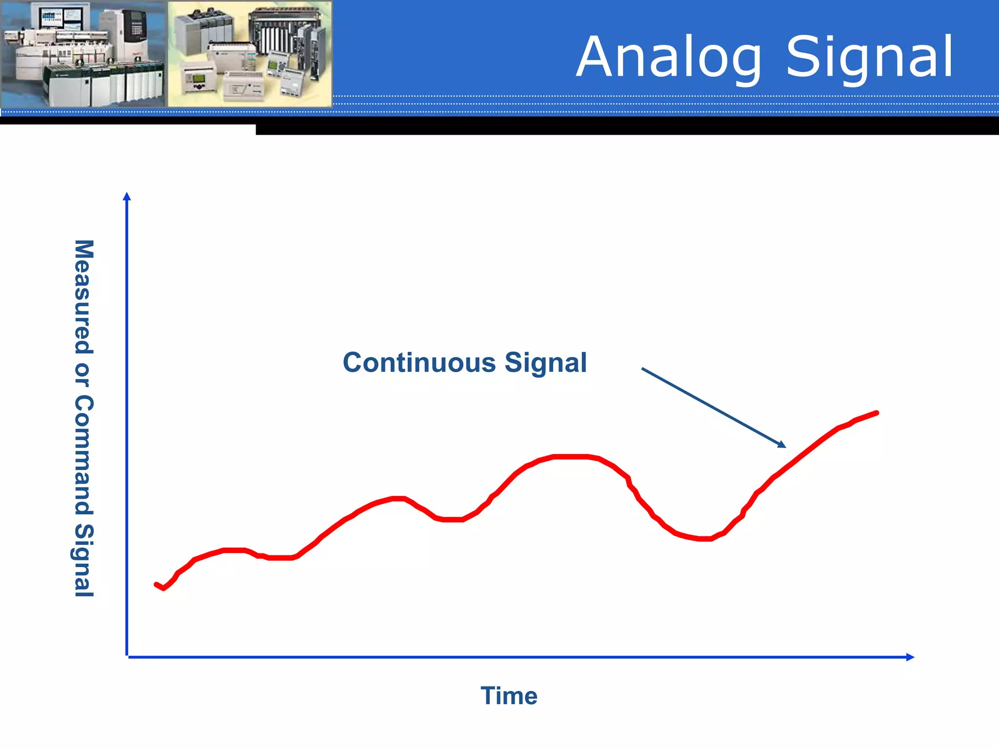
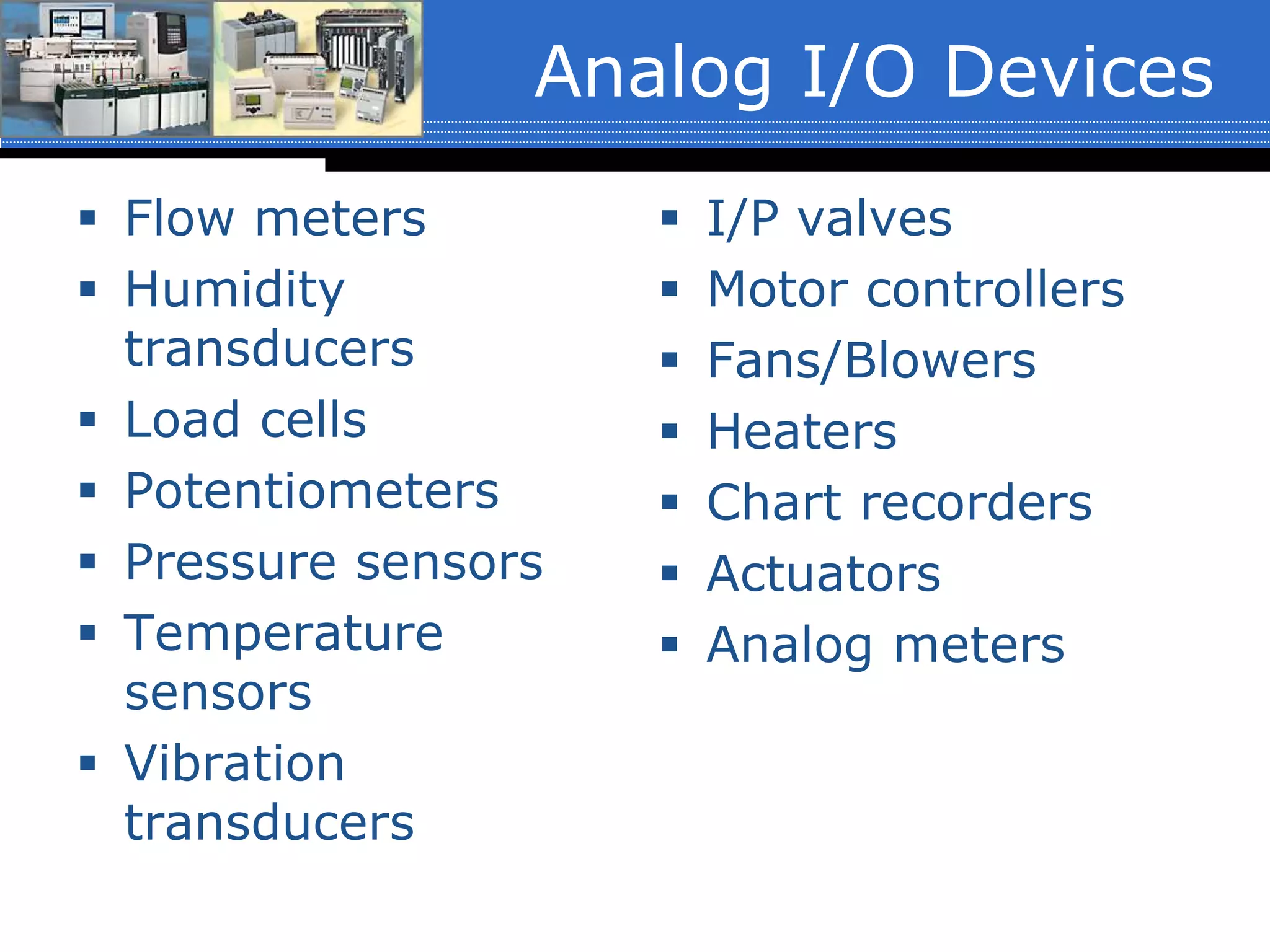
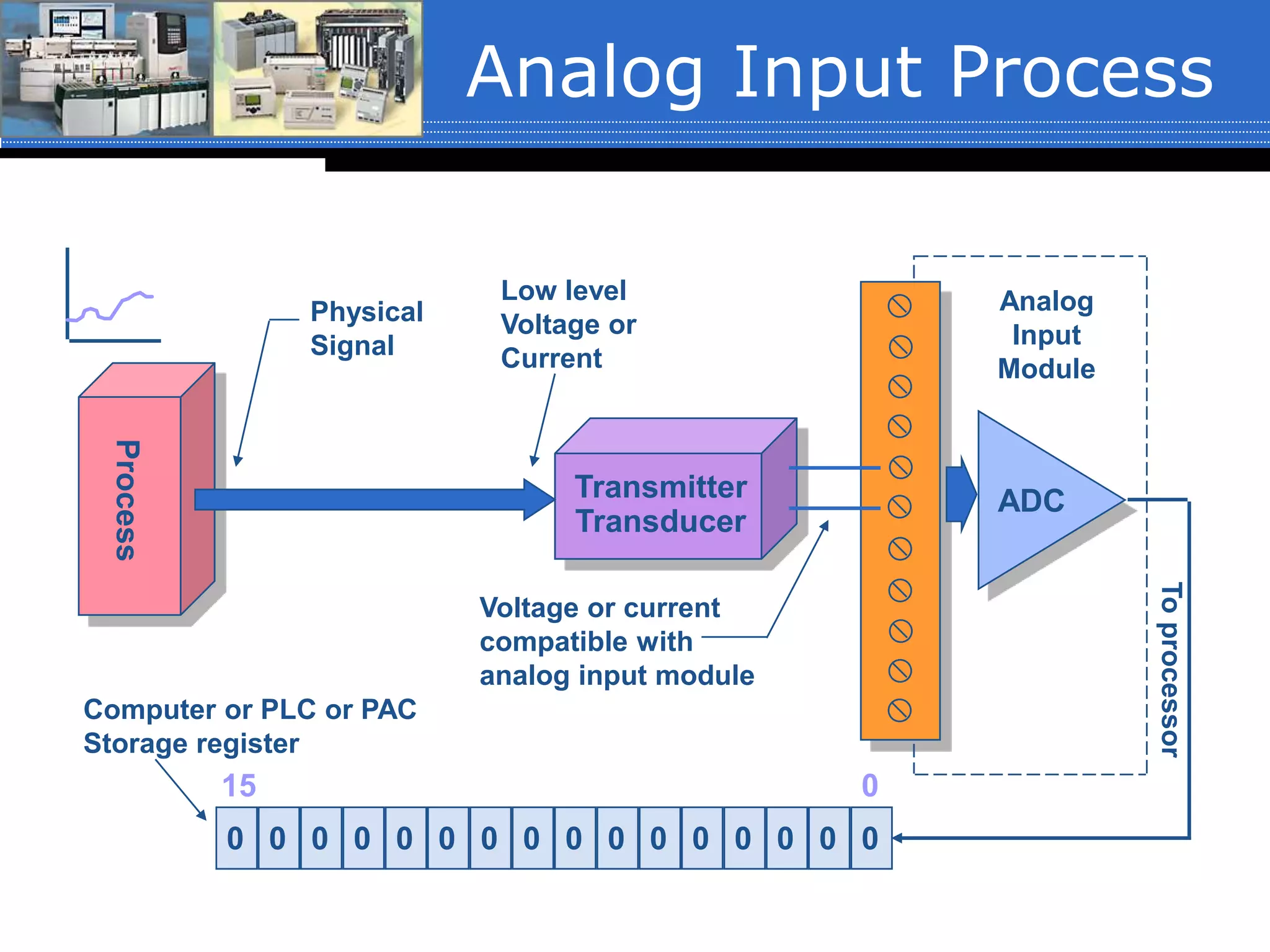
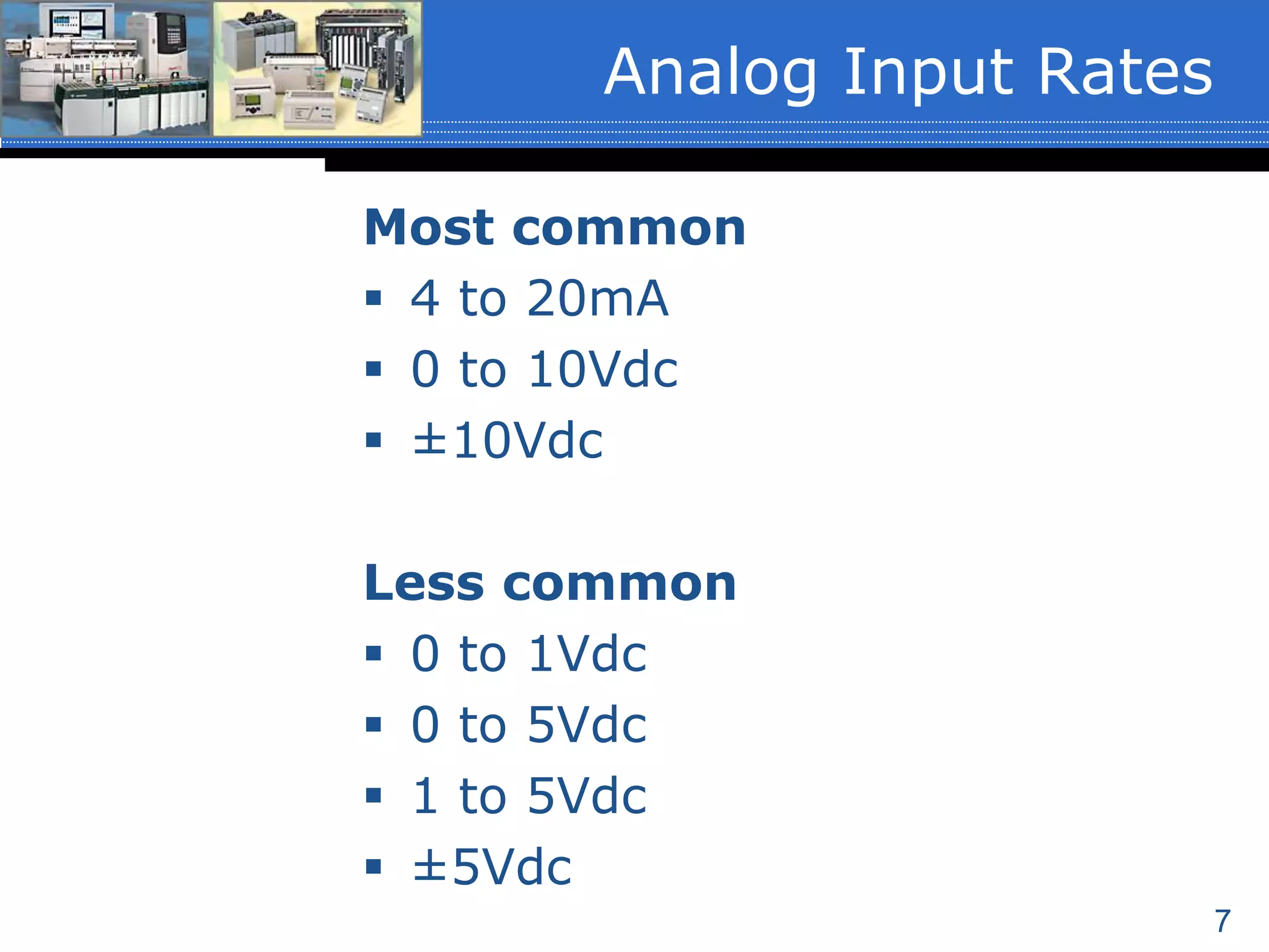
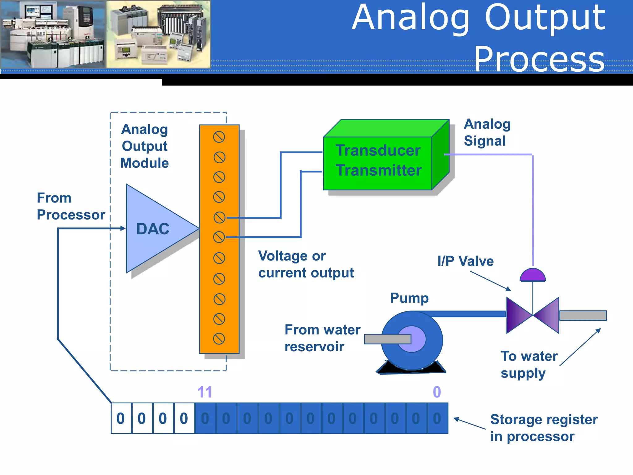
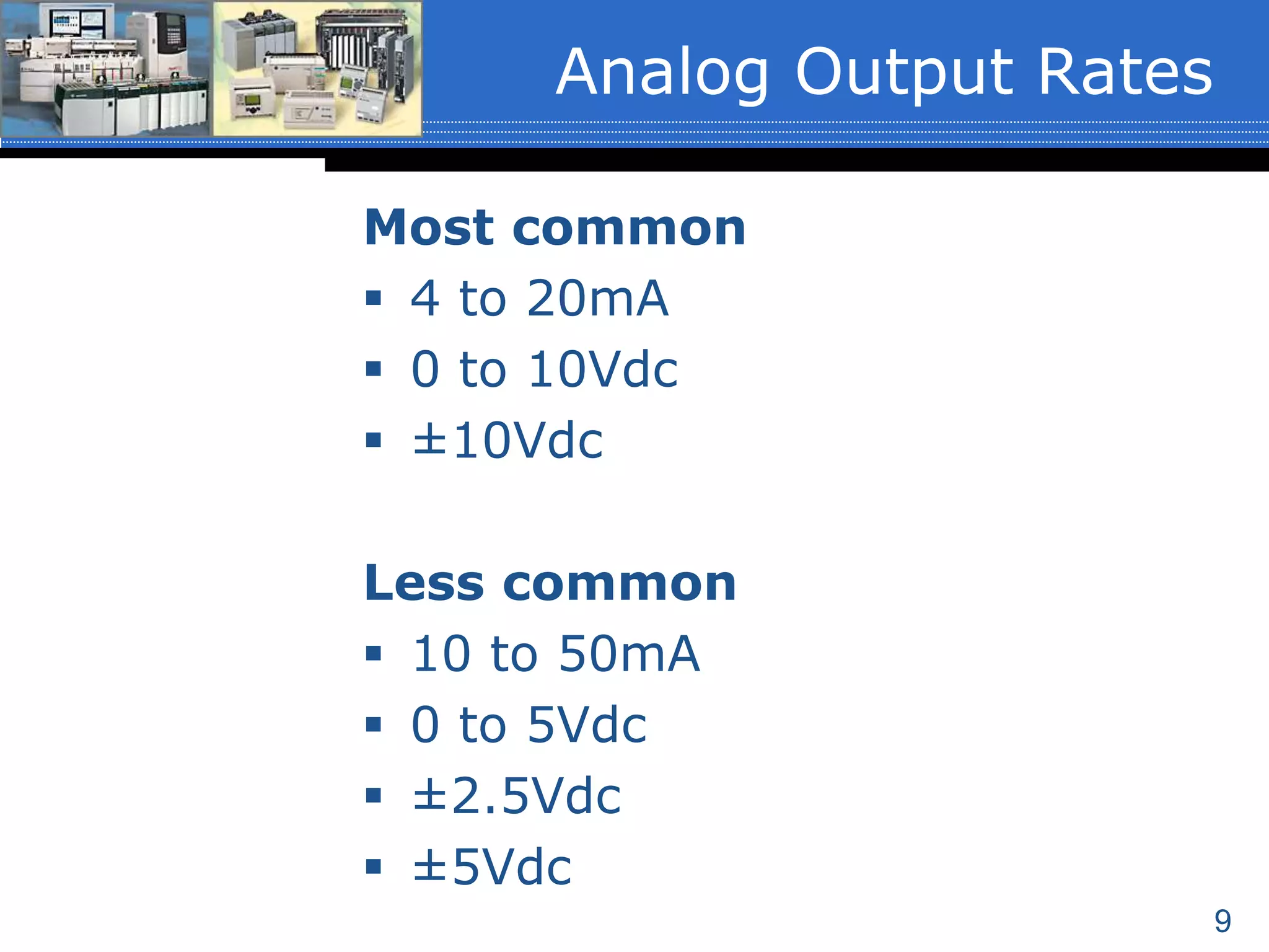
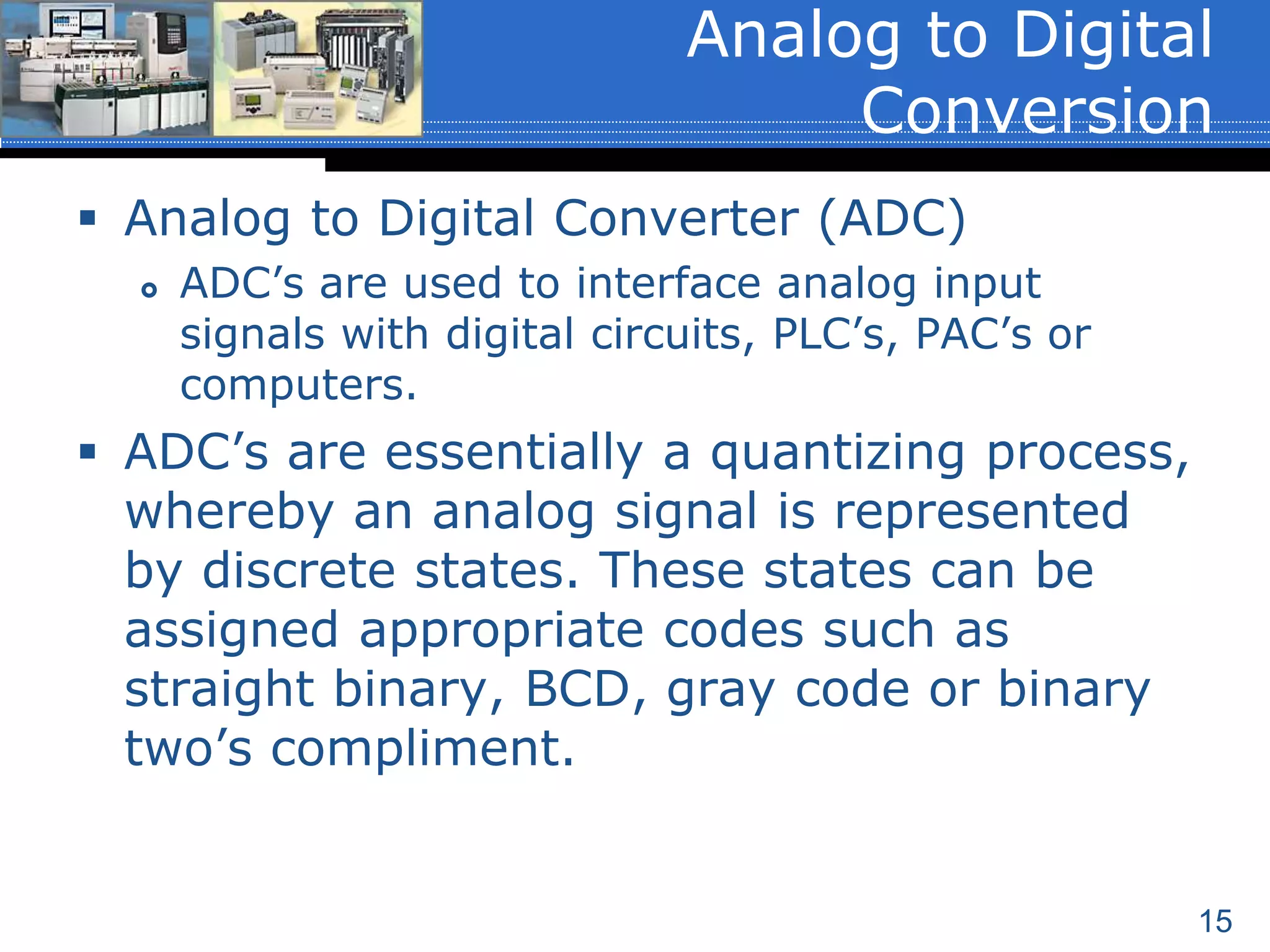
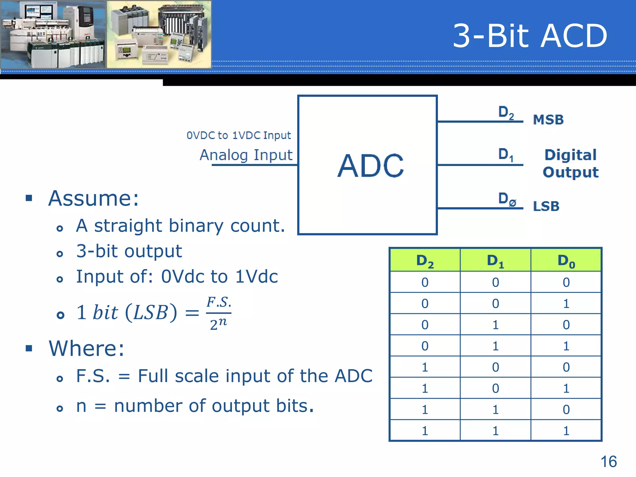
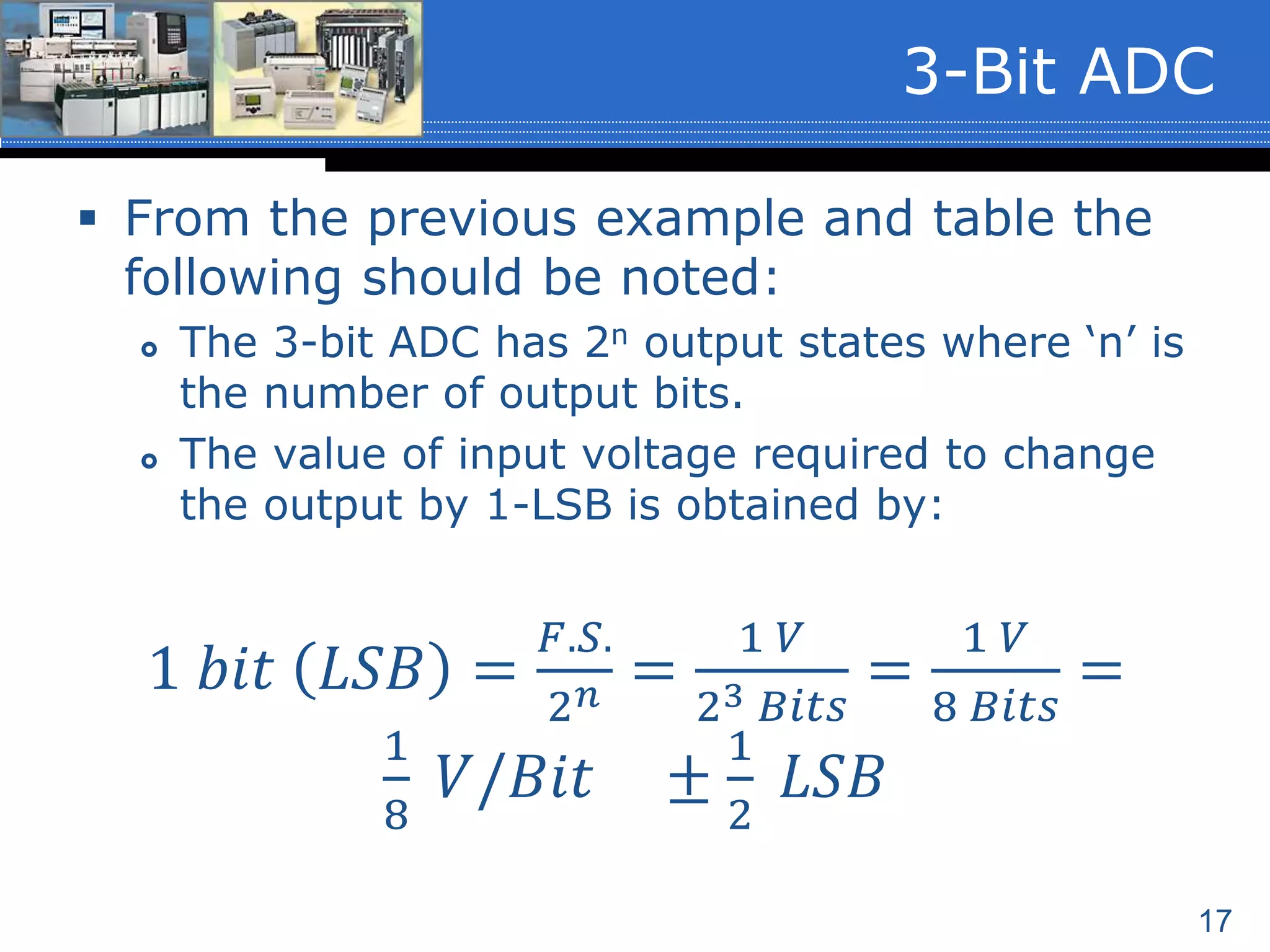
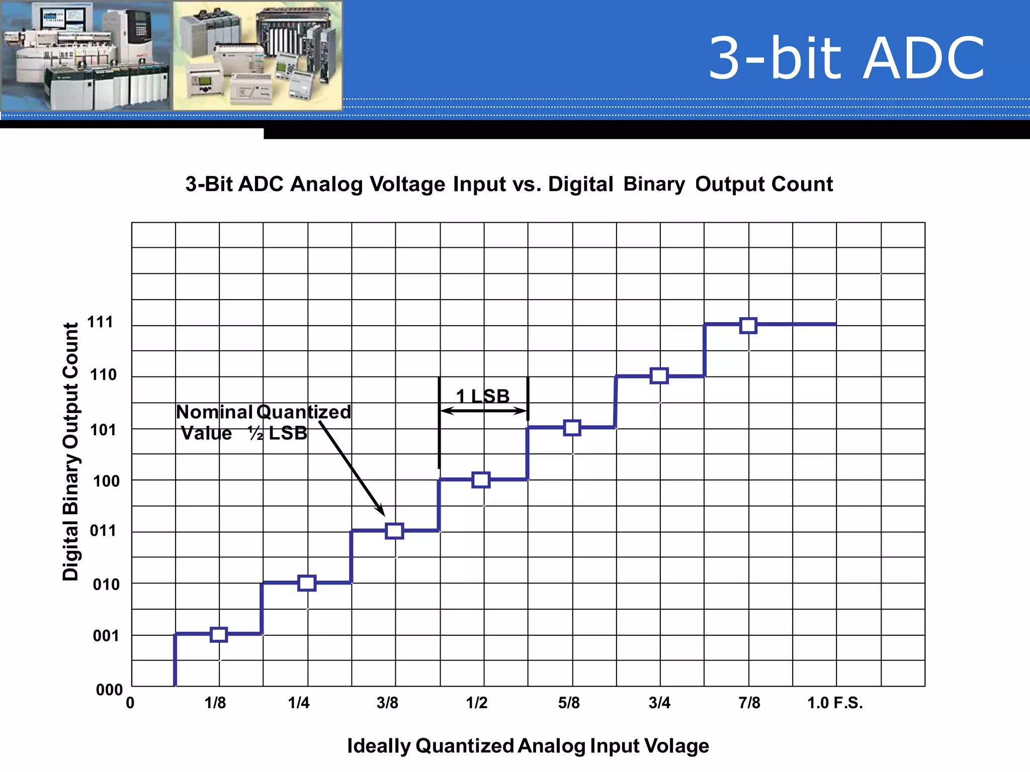
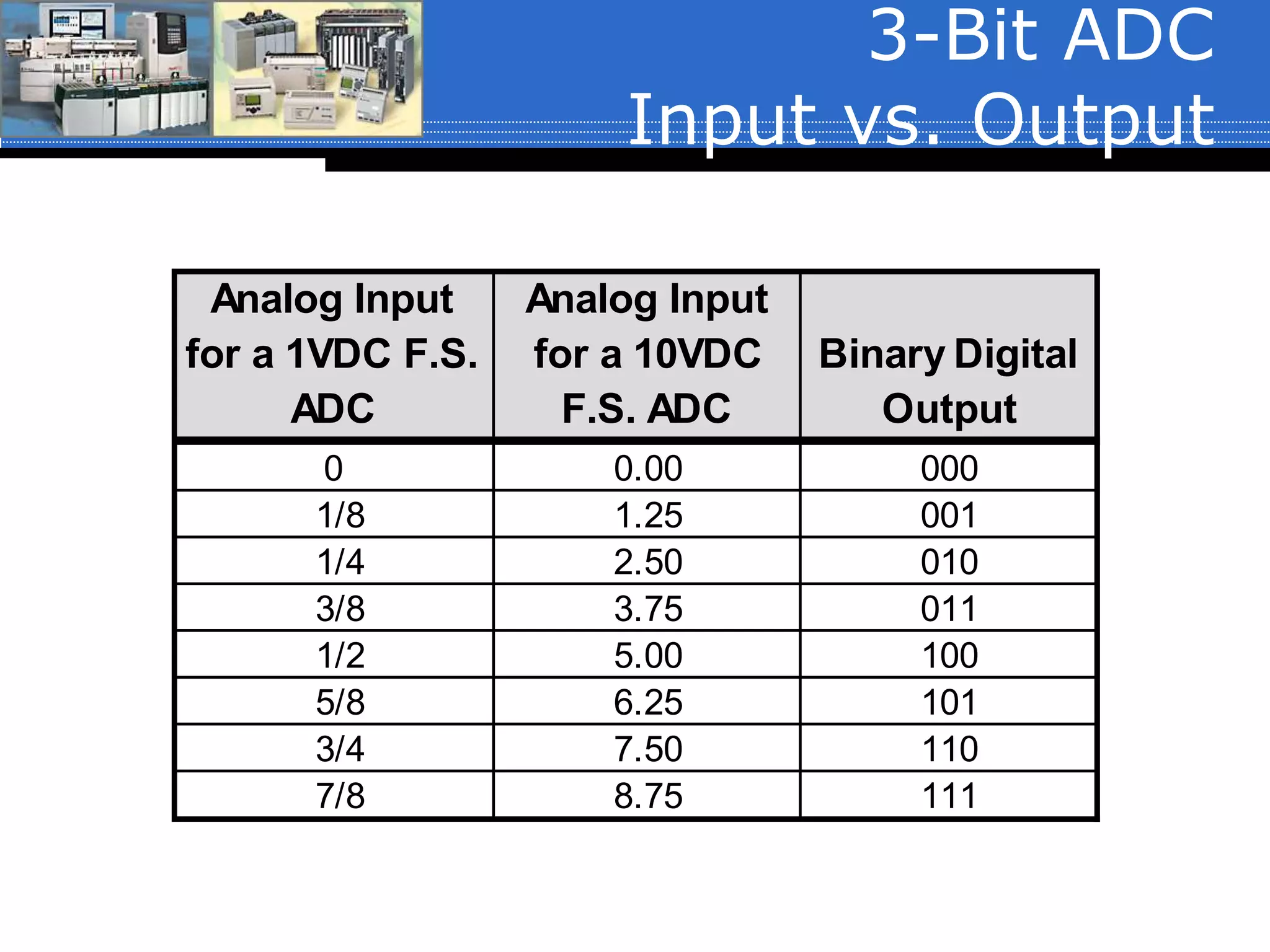
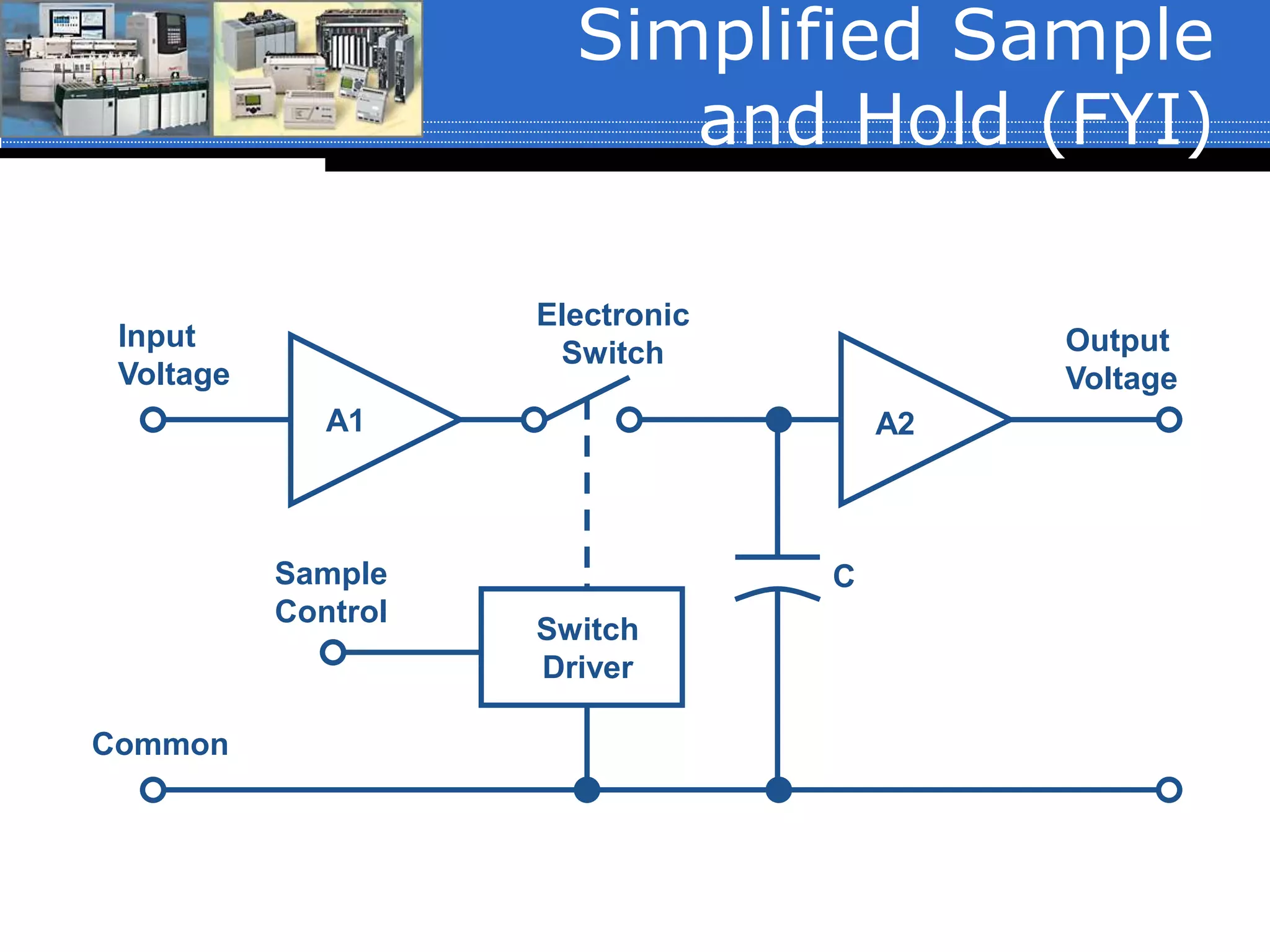
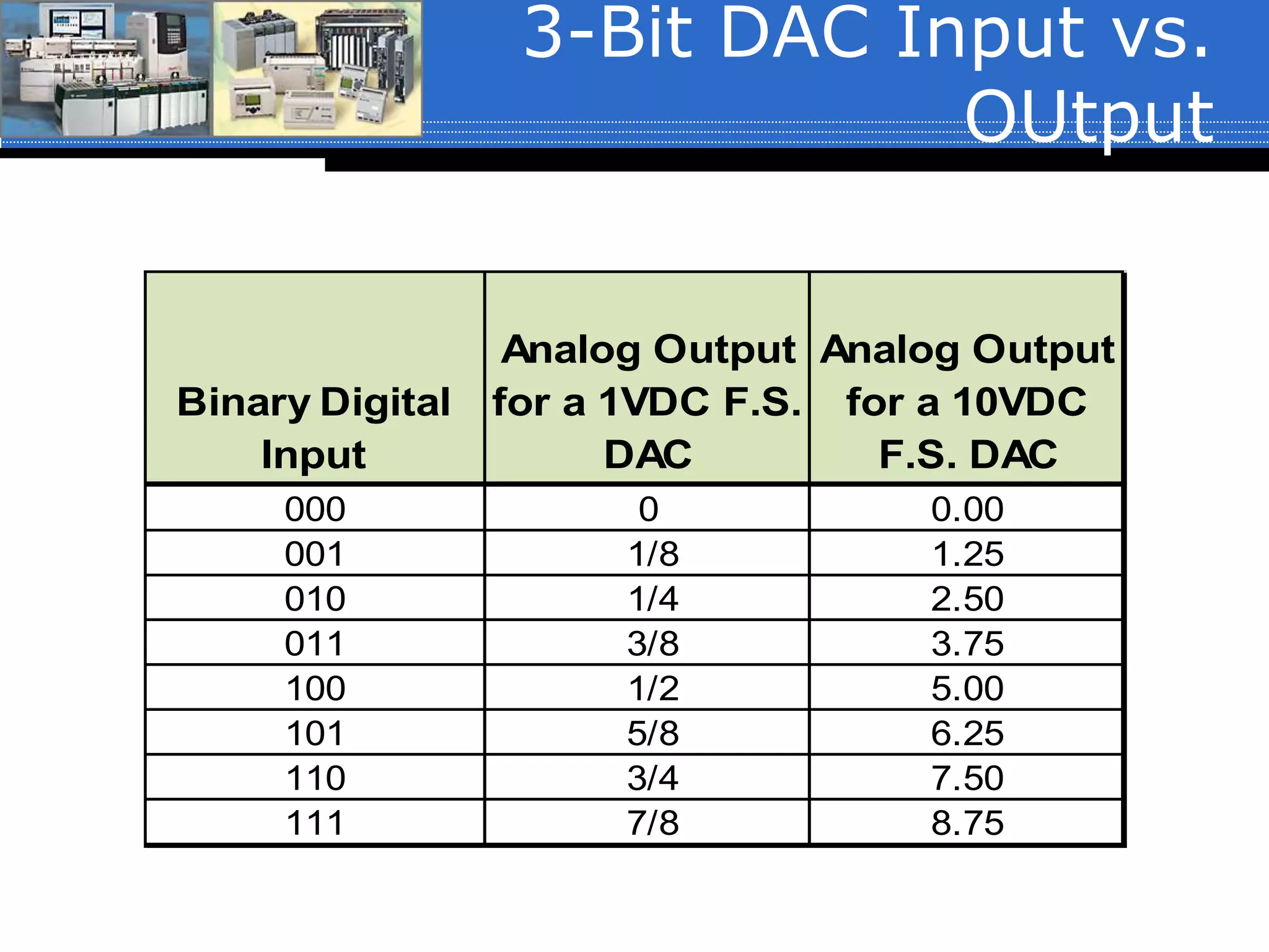
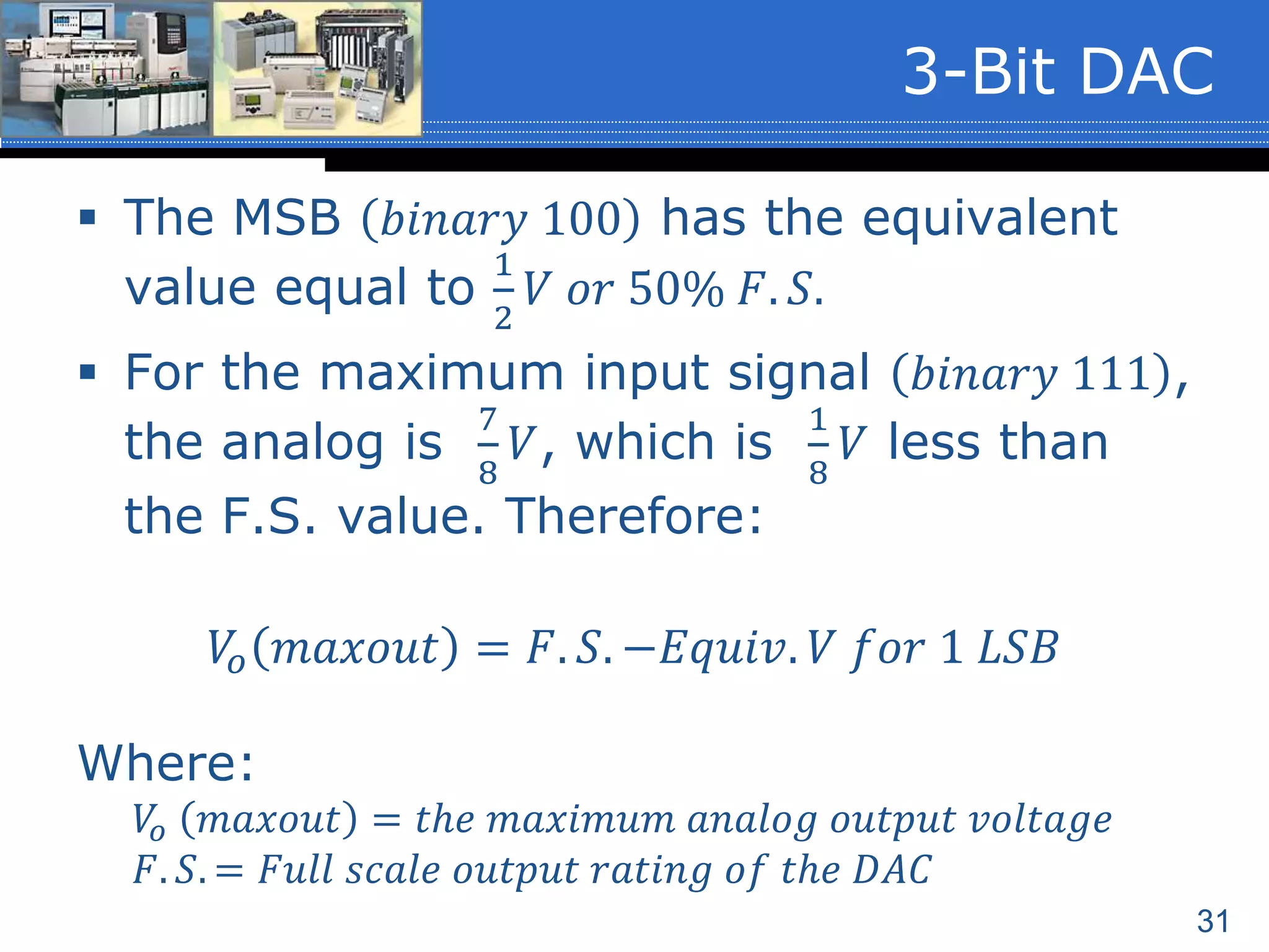
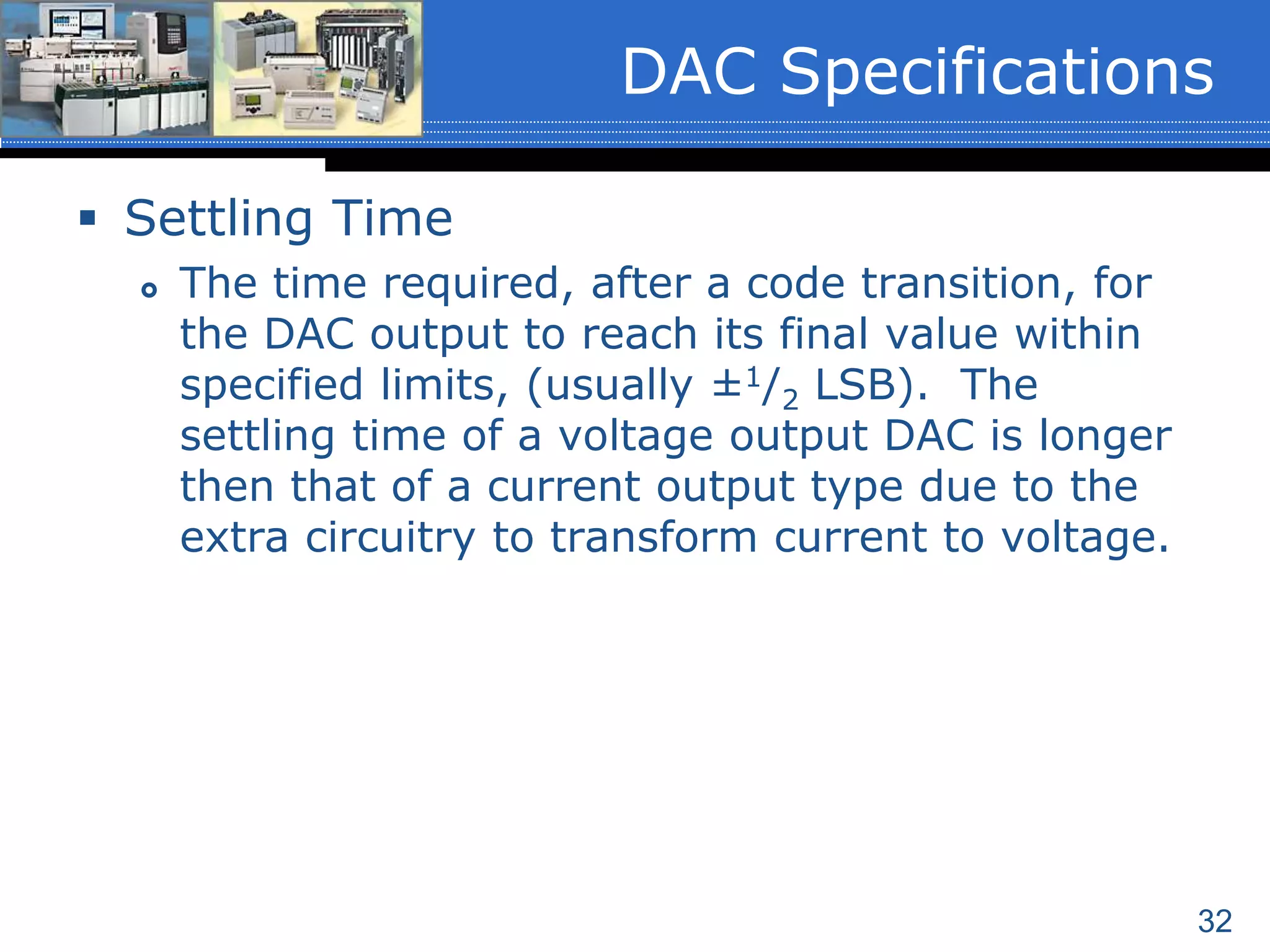
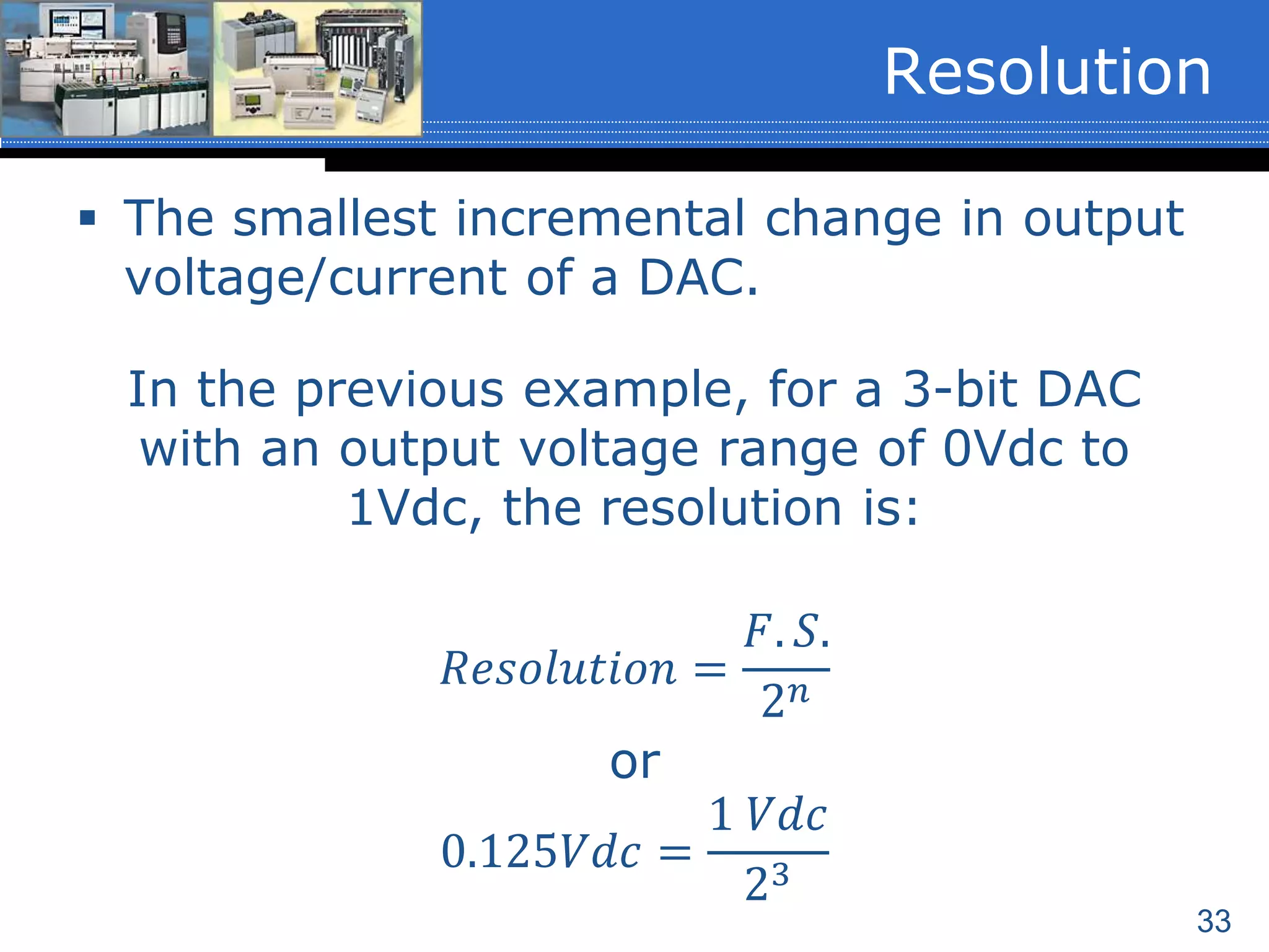
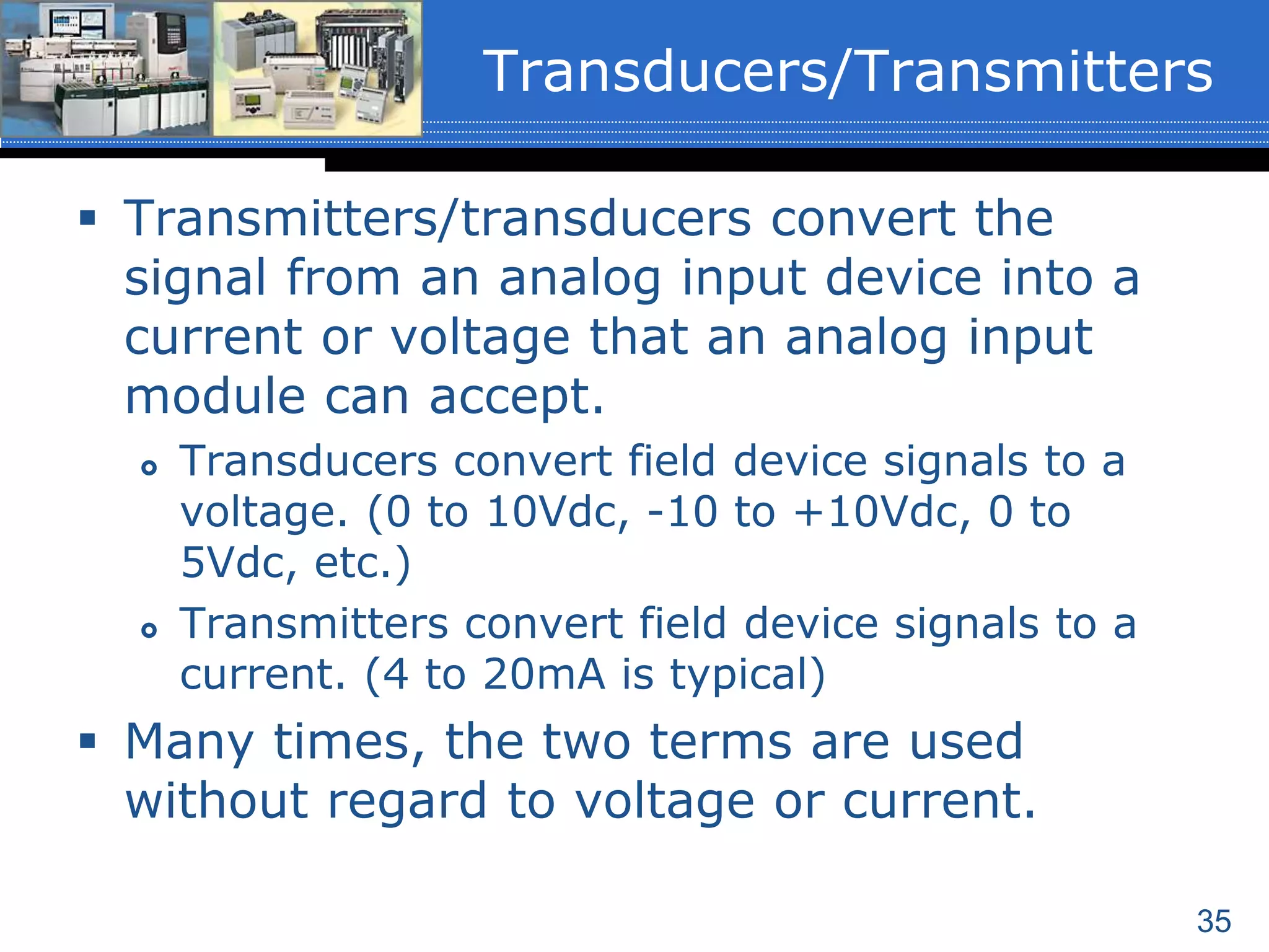
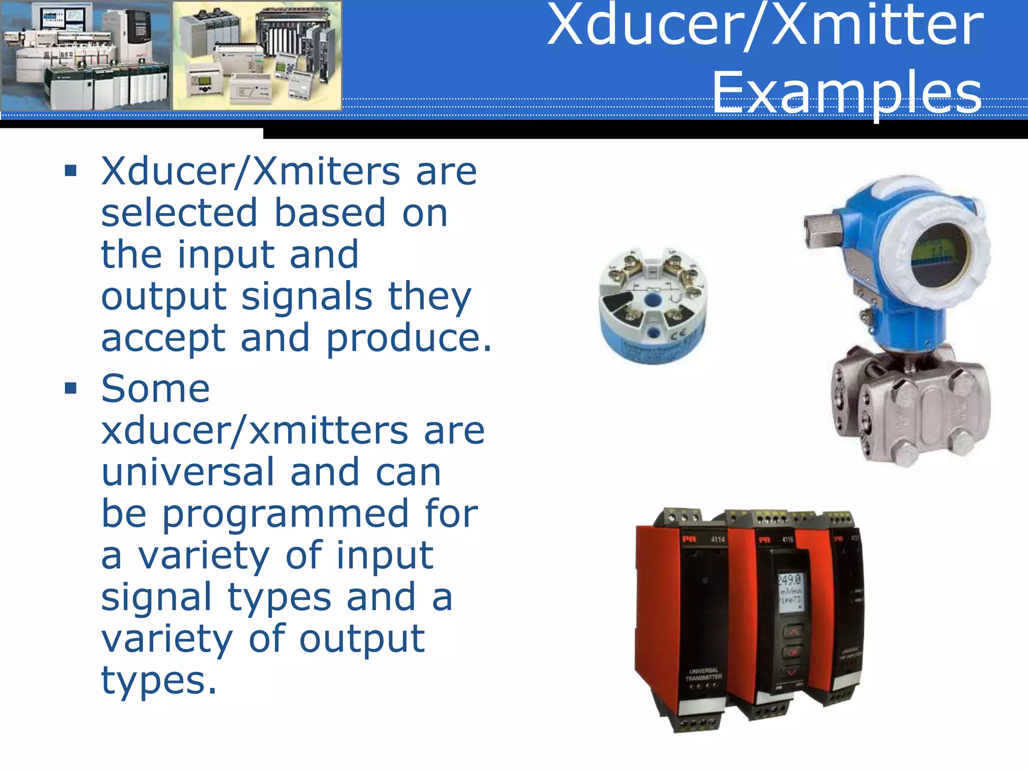
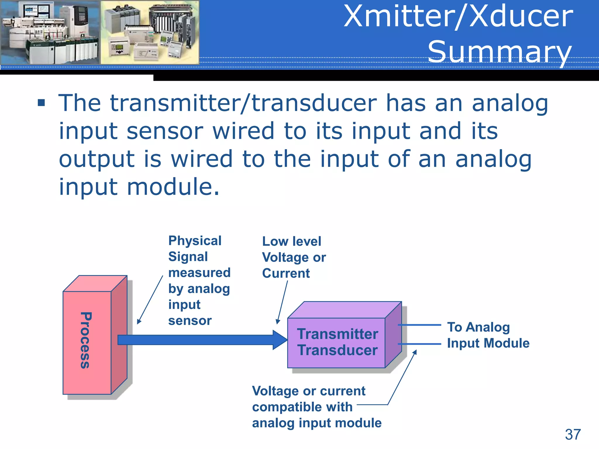
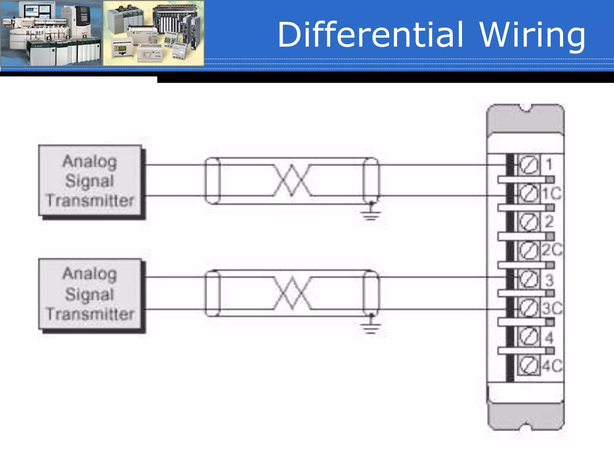
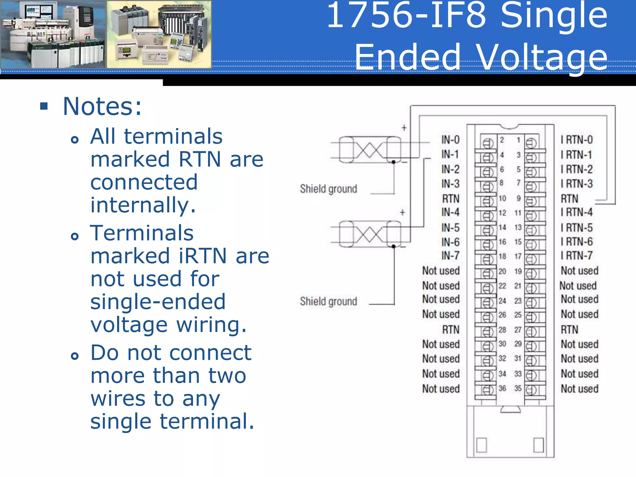
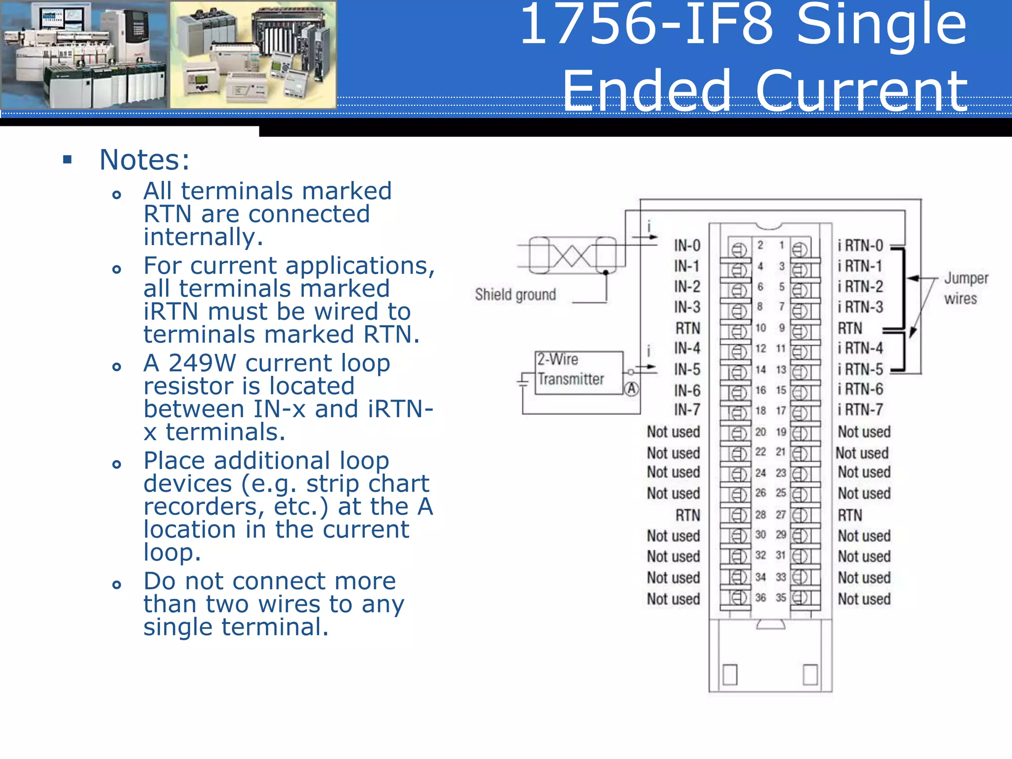
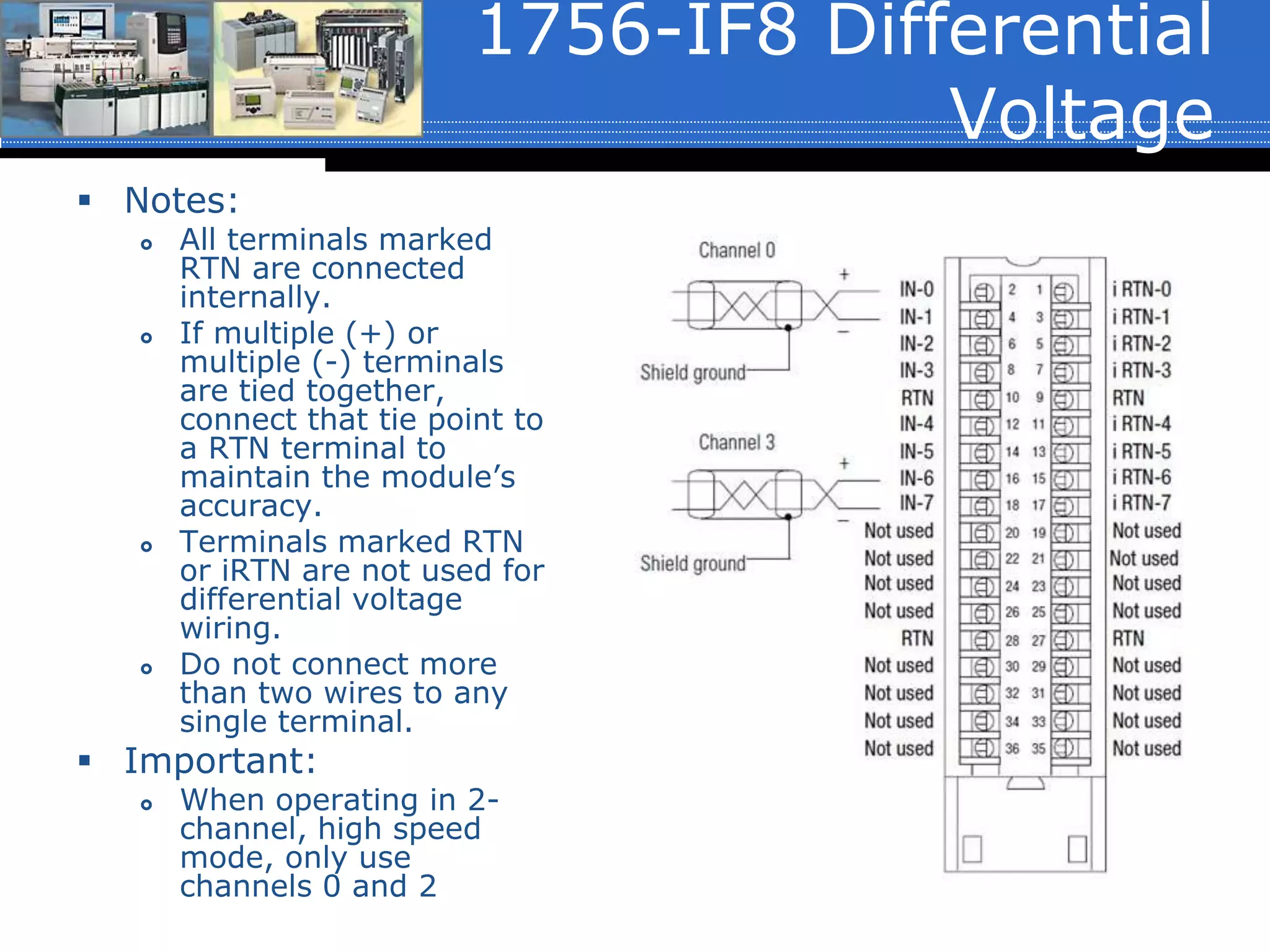
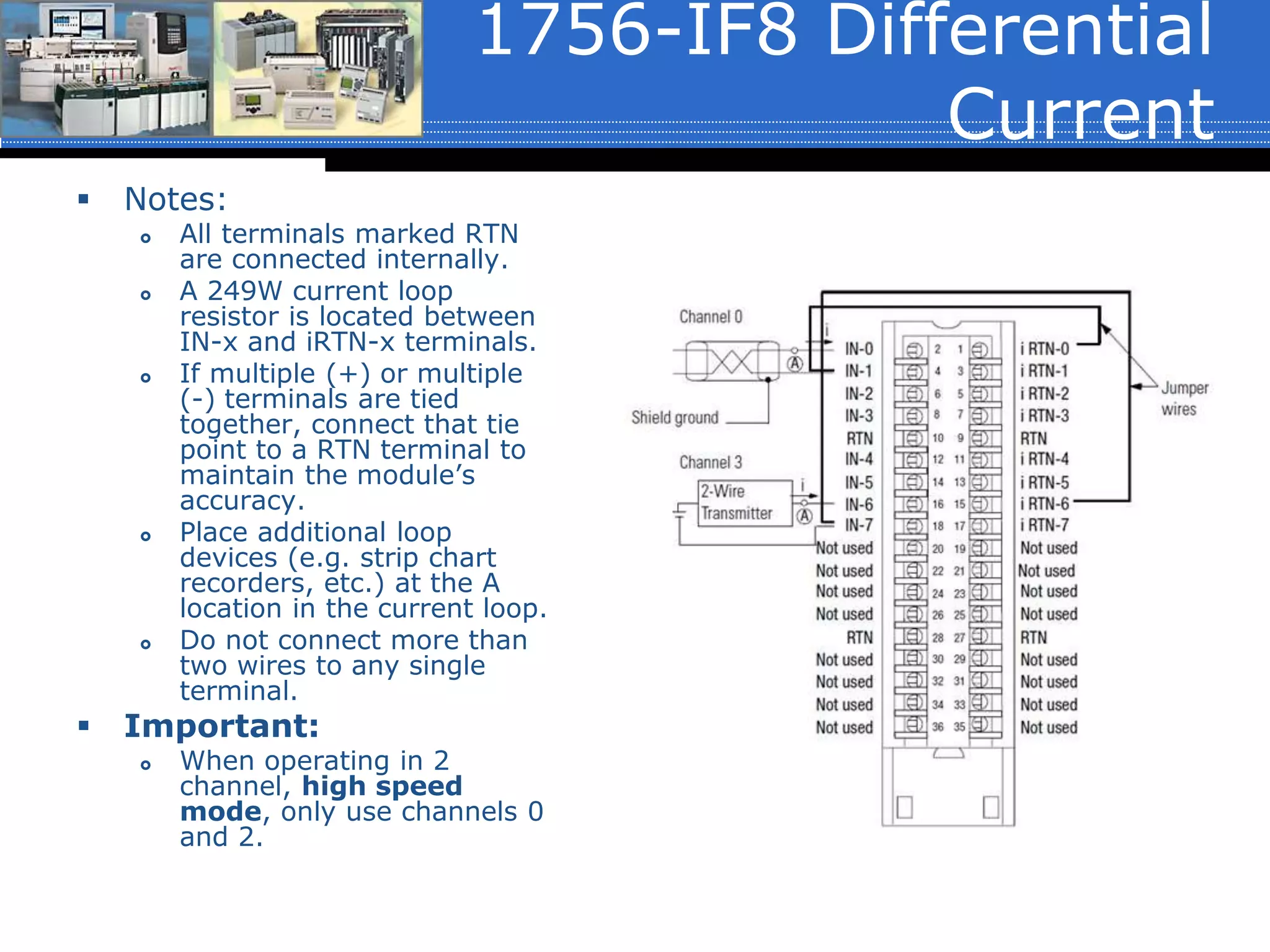
Analog Control
Supplemental material
Chapter 12 & 13
3
 Discrete signals only have two states; ON
or OFF.
 Analog signals have an infinite number of
states. It can be totally ON, totally OFF or
anything in-between.
 PLC’s/PAC’s use analog I/O modules in
applications where the field device signals
are continuously varying.
Overview
Analog Signal
Continuous Signal
Time
MeasuredorCommandSignal
Analog I/O Devices
 Flow meters
 Humidity
transducers
 Load cells
 Potentiometers
 Pressure sensors
 Temperature
sensors
 Vibration
transducers
 I/P valves
 Motor controllers
 Fans/Blowers
 Heaters
 Chart recorders
 Actuators
 Analog meters
Analog Input ProcessProcess
Transducer
Transmitter ADC
0000000000000000
15 0
Physical
Signal
Low level
Voltage or
Current
Voltage or current
compatible with
analog input module
Analog
Input
Module
Toprocessor
Computer or PLC or PAC
Storage register
7
Most common
 4 to 20mA
 0 to 10Vdc
 ±10Vdc
Less common
 0 to 1Vdc
 0 to 5Vdc
 1 to 5Vdc
 ±5Vdc
Analog Input Rates
Analog Output
Process
DAC
Analog
Output
Module
0000000000000000
11 0
Transducer
From
Processor
Storage register
in processor
Voltage or
current output
Analog
Signal
From water
reservoir
To water
supply
I/P Valve
Pump
Transmitter
9
Most common
 4 to 20mA
 0 to 10Vdc
 ±10Vdc
Less common
 10 to 50mA
 0 to 5Vdc
 ±2.5Vdc
 ±5Vdc
Analog Output Rates
10
 Analog signals are encoded by
representing them in a binary word, as a
binary number.
 The binary number corresponds to the
value of the analog signal at a given
instant in time.
Analog Signals
11
 Analog input signals are represented in
digital format through the process of
sampling the continuous analog waveform
at regular intervals of time and then
performing an analog to digital
conversion.
 If the sample rate is twice the rate of the
analog signal change, the signal can be
exactly reproduced. (Actually, analog
signals can never be perfectly produced.
There will always be some error).
Sampling
12
 The process of assigning a discrete binary
number to each sample introduces an
error known as quantization error.
 Quantization is an unavoidable error
resulting from the difference between the
actual value of the analog sample and the
nearest value encoded by one of the
binary numbers.
Sampling
Sampling
http://www.videomaker.com/article/14524/
Sampling
http://www.music-production-school.com/pro_tools_software_article.shtml
15
 Analog to Digital Converter (ADC)
 ADC’s are used to interface analog input
signals with digital circuits, PLC’s, PAC’s or
computers.
 ADC’s are essentially a quantizing process,
whereby an analog signal is represented
by discrete states. These states can be
assigned appropriate codes such as
straight binary, BCD, gray code or binary
two’s compliment.
Analog to Digital
Conversion
16
 Assume:
 A straight binary count.
 3-bit output
 Input of: 0Vdc to 1Vdc
 1 𝑏𝑖𝑡 𝐿𝑆𝐵 =
𝐹.𝑆.
2 𝑛
 Where:
 F.S. = Full scale input of the ADC
 n = number of output bits.
3-Bit ACD
D2 D1 D0
0 0 0
0 0 1
0 1 0
0 1 1
1 0 0
1 0 1
1 1 0
1 1 1
17
 From the previous example and table the
following should be noted:
 The 3-bit ADC has 2n output states where ‘n’ is
the number of output bits.
 The value of input voltage required to change
the output by 1-LSB is obtained by:
3-Bit ADC
1 𝑏𝑖𝑡 𝐿𝑆𝐵 =
𝐹.𝑆.
2 𝑛 =
1 𝑉
23 𝐵𝑖𝑡𝑠
=
1 𝑉
8 𝐵𝑖𝑡𝑠
=
1
8
𝑉/𝐵𝑖𝑡 ±
1
2
𝐿𝑆𝐵
3-bit ADCDigitalBinaryOutputCount
Ideally QuantizedAnalog Input Volage
3-Bit ADC Analog Voltage Input vs. Digital Bianry Output Count
000
100
011
010
001
111
110
101
1/8 7/83/45/81/23/81/40 1.0 F.S.
1 LSB
NominalQuantized
Value ½ LSB
Binary
3-Bit ADC
Input vs. Output
Analog Input
for a 1VDC F.S.
ADC
Analog Input
for a 10VDC
F.S. ADC
Binary Digital
Output
0 0.00 000
1/8 1.25 001
1/4 2.50 010
3/8 3.75 011
1/2 5.00 100
5/8 6.25 101
3/4 7.50 110
7/8 8.75 111
20
 Analog input values shown represent the center
point of the analog values for each output word,
with transition points ±½ LSB from the center
points. The quantizing error or uncertainty is thus
½ LSB.
 The MSB (1002) output corresponds to ½ V on
the input which is half of the F.S. input range.
The largest output word (1112) corresponds to
7/8 V and F.S.
3-Bit ADC
𝑉𝑜 𝑚𝑎𝑥𝑜𝑢𝑡 = 𝐹. 𝑆 − 1 𝐿𝑆𝐵
or
1 𝑉𝑑𝑐 −
1
8
𝑉𝑑𝑐 =
7
8
𝑉𝑑𝑐
21
 An ADC requires a certain length of time,
called conversion time, to change an
analog signal into the corresponding
digital signal.
 If the analog signal changes during the
conversion time the converter output may
be in error. To prevent this a sample and
hold circuit is used.
Sampling Concepts
Simplified Sample
and Hold (FYI)
Input
Voltage
A1 A2
Electronic
Switch
Switch
Driver
C
Output
Voltage
Common
Sample
Control
23
 Conversion Time
 The total time required to completely convert
an analog input current or voltage to a digital
output. The time is affected by the propagation
delay in the various circuits. It may be
specified as a number of conversions per
second.
 This is one of the most important specifications
to be considered when selecting an ADC.
Converters having more output bits usually
require more time.
ADC Characteristics
24
 Resolution
 The amount of input voltage required to
increment the output by one LSB. The
resolution is determined by the number of
output bits. It is specified in terms of the
number of output bits or as one part per
number of output states. As an example: the
resolution of an 8-bit converter is specified as
either 8-bits or 1 out of 256
1
28 =
1
256
 Example:
 The resolution of our 3-bit ADC is 1 out of 8
1
23 =
1
8
ADC Characteristics
25
 Digital to Analog Converter (DAC)
 Digital systems can be used to transmit analog
signals. This is accomplished by using a DAC
whereby a given digital signal is transformed
into its equivalent analog signal.
 Three categories
 Current output
 Voltage output
 Multiplying type
Digital to Analog
Converter (DAC)
26
 The DAC process can be viewed as finding
the equivalent weight of and object (less
then one unit) with weights in
geometrically proportional units, such as
1/8, 1/4 and 1/2. By using these weights in
various combinations, 8 different
measurements ranging from zero units to
7/8 units can be obtained.
Concept & Transfer
Function
27
 Assume:
 A straight binary count.
 3-Bit output
 Output of: 0Vdc to 1Vdc
 Where:
 F.S. = Full scale input of
DAC
 n = Number of output
bits.
3-Bit DAC
D2 D1 D0
0 0 0
0 0 1
0 1 0
0 1 1
1 0 0
1 0 1
1 1 0
1 1 1
28
 By the previous example and table the
following should be noted:
 The 3-Bit DAC has eight 2 𝑛 = 8 possible input
combinations 𝑛 = 𝑛𝑢𝑚𝑏𝑒𝑟 𝑜𝑓 𝑖𝑛𝑝𝑢𝑡 𝑏𝑖𝑡𝑠 , ranging
from 0002 𝑡𝑜 1112.
 If the F.S. analog voltage is 1Vdc, the smallest
unit 𝐿𝑆𝐵 001 is equivalent to
1
8
𝑉. No voltage or
step smaller can be identified by this DAC
(resolution).
3-Bit DAC
3-Bit DAC Output
Voltage vs. Binary
3-Bit DAC Output Voltage vs. Binary Count
0
1/8
1/4
3/8
1/2
5/8
3/4
7/8
1
000 001 010 011 100 101 110 111
Binary Input Count
OutputVoltageChange
3-Bit DAC Input vs.
OUtput
Binary Digital
Input
Analog Output
for a 1VDC F.S.
DAC
Analog Output
for a 10VDC
F.S. DAC
000 0 0.00
001 1/8 1.25
010 1/4 2.50
011 3/8 3.75
100 1/2 5.00
101 5/8 6.25
110 3/4 7.50
111 7/8 8.75
31
 The MSB 𝑏𝑖𝑛𝑎𝑟𝑦 100 has the equivalent
value equal to
1
2
𝑉 𝑜𝑟 50% 𝐹. 𝑆.
 For the maximum input signal 𝑏𝑖𝑛𝑎𝑟𝑦 111 ,
the analog is
7
8
𝑉, which is
1
8
𝑉 less than
the F.S. value. Therefore:
𝑉𝑜 𝑚𝑎𝑥𝑜𝑢𝑡 = 𝐹. 𝑆. −𝐸𝑞𝑢𝑖𝑣. 𝑉 𝑓𝑜𝑟 1 𝐿𝑆𝐵
Where:
𝑉𝑜 𝑚𝑎𝑥𝑜𝑢𝑡 = 𝑡ℎ𝑒 𝑚𝑎𝑥𝑖𝑚𝑢𝑚 𝑎𝑛𝑎𝑙𝑜𝑔 𝑜𝑢𝑡𝑝𝑢𝑡 𝑣𝑜𝑙𝑡𝑎𝑔𝑒
𝐹. 𝑆. = 𝐹𝑢𝑙𝑙 𝑠𝑐𝑎𝑙𝑒 𝑜𝑢𝑡𝑝𝑢𝑡 𝑟𝑎𝑡𝑖𝑛𝑔 𝑜𝑓 𝑡ℎ𝑒 𝐷𝐴𝐶
3-Bit DAC
32
 Settling Time
 The time required, after a code transition, for
the DAC output to reach its final value within
specified limits, (usually ±1/2 LSB). The
settling time of a voltage output DAC is longer
then that of a current output type due to the
extra circuitry to transform current to voltage.
DAC Specifications
33
 The smallest incremental change in output
voltage/current of a DAC.
In the previous example, for a 3-bit DAC
with an output voltage range of 0Vdc to
1Vdc, the resolution is:
𝑅𝑒𝑠𝑜𝑙𝑢𝑡𝑖𝑜𝑛 =
𝐹. 𝑆.
2 𝑛
or
0.125𝑉𝑑𝑐 =
1 𝑉𝑑𝑐
23
Resolution
Transducers/Transmitters
Single-Ended vs Differential
Analog Input Wiring
35
 Transmitters/transducers convert the
signal from an analog input device into a
current or voltage that an analog input
module can accept.
 Transducers convert field device signals to a
voltage. (0 to 10Vdc, -10 to +10Vdc, 0 to
5Vdc, etc.)
 Transmitters convert field device signals to a
current. (4 to 20mA is typical)
 Many times, the two terms are used
without regard to voltage or current.
Transducers/Transmitters
Xducer/Xmitter
Examples
 Xducer/Xmiters are
selected based on
the input and
output signals they
accept and produce.
 Some
xducer/xmitters are
universal and can
be programmed for
a variety of input
signal types and a
variety of output
types.
37
 The transmitter/transducer has an analog
input sensor wired to its input and its
output is wired to the input of an analog
input module.
Xmitter/Xducer
Summary
Process
Transducer
Transmitter
Physical
Signal
measured
by analog
input
sensor
Low level
Voltage or
Current
Voltage or current
compatible with
analog input module
To Analog
Input Module
38
 Xducers/xmitters are wired in a circuit
most often called a ‘current loop’ or a
‘voltage loop’.
 The xducer/xmitter might require a power
supply; ‘loop power’.
 Other xducers/xmitters might supply their
own ‘loop power’.
 Always refer to the manufacturers
specifications and wiring diagrams.
Wiring Configuration
 These xducers
/ xmitters
require loop
power.
 Xducers /
xmitters that
do not require
loop power will
be wired
directly to the
module.
2- Wire Transducer/Transmitter
3- Wire Transducer/Transmitter
4- Wire Transducer/Transmitter
Xducer/xmitter
Xducer/xmitter
Xducer/xmitter
40
 Analog input modules accept analog
signals.
 These inputs are referred to as channels.
 The inputs can be voltage or current.
 Some input modules require configuration
to set if the module or individual channels
can accept voltage or current. Depending
on the module, configuration can be done:
 Through the programming software.
 With DIP switch settings.
 Input wiring arrangement.
Analog Input Modules
41
 Most analog input modules can be wired
single-ended or differential.
 The methods are usually defined by the
type of input devices and/or the physical
location of the devices.
 Single-ended wiring is usually used in low
noise (electrical noise) environments and
differential is usually used in areas where
there is a lot of Electro-Magnetic
Interference (EMI) (a.k.a. Noise)
Single-Ended vs
Differential
42
 Measurements taken with an analog input
module that are single-ended, take the
voltage or current difference between a
single wire and ground.
 The noise is only on the positive wire and
therefore is measured along with the
output signal from the input sensor.
 In areas where high levels of electrical
noise are present, the noise could cause
measurement errors.
Single-Ended
43
 Measurements taken with an analog input
module that are differential are “floating”,
there is no ground reference.
 The measurement is taken as the voltage
difference between the two wires.
 In areas where high levels of electrical
noise are present, the noise is added to
both wires, in-phase, and can than be
filtered by the common mode rejection of
the module.
Differential
Analog Input Wiring
 The diagram
shows single
ended wiring of
several xducers
/ xmitters
wired to an
analog input
module.
Xducer/xmitter
Xducer/xmitter
Xducer/xmitter
Xducer/xmitter
Single Ended Wiring
Differential Wiring
1756-IF8 Single
Ended Voltage
 Notes:
 All terminals
marked RTN are
connected
internally.
 Terminals
marked iRTN are
not used for
single-ended
voltage wiring.
 Do not connect
more than two
wires to any
single terminal.
1756-IF8 Single
Ended Current
 Notes:
 All terminals marked
RTN are connected
internally.
 For current applications,
all terminals marked
iRTN must be wired to
terminals marked RTN.
 A 249W current loop
resistor is located
between IN-x and iRTN-
x terminals.
 Place additional loop
devices (e.g. strip chart
recorders, etc.) at the A
location in the current
loop.
 Do not connect more
than two wires to any
single terminal.
1756-IF8 Differential
Voltage
 Notes:
 All terminals marked
RTN are connected
internally.
 If multiple (+) or
multiple (-) terminals
are tied together,
connect that tie point to
a RTN terminal to
maintain the module’s
accuracy.
 Terminals marked RTN
or iRTN are not used for
differential voltage
wiring.
 Do not connect more
than two wires to any
single terminal.
 Important:
 When operating in 2-
channel, high speed
mode, only use
channels 0 and 2
1756-IF8 Differential
Current
 Notes:
 All terminals marked RTN
are connected internally.
 A 249W current loop
resistor is located between
IN-x and iRTN-x terminals.
 If multiple (+) or multiple
(-) terminals are tied
together, connect that tie
point to a RTN terminal to
maintain the module’s
accuracy.
 Place additional loop
devices (e.g. strip chart
recorders, etc.) at the A
location in the current loop.
 Do not connect more than
two wires to any single
terminal.
 Important:
 When operating in 2
channel, high speed
mode, only use channels 0
and 2.

03 analog control_sp17

  • 1.
  • 2.
  • 3.
    3  Discrete signalsonly have two states; ON or OFF.  Analog signals have an infinite number of states. It can be totally ON, totally OFF or anything in-between.  PLC’s/PAC’s use analog I/O modules in applications where the field device signals are continuously varying. Overview
  • 4.
  • 5.
    Analog I/O Devices Flow meters  Humidity transducers  Load cells  Potentiometers  Pressure sensors  Temperature sensors  Vibration transducers  I/P valves  Motor controllers  Fans/Blowers  Heaters  Chart recorders  Actuators  Analog meters
  • 6.
    Analog Input ProcessProcess Transducer TransmitterADC 0000000000000000 15 0 Physical Signal Low level Voltage or Current Voltage or current compatible with analog input module Analog Input Module Toprocessor Computer or PLC or PAC Storage register
  • 7.
    7 Most common  4to 20mA  0 to 10Vdc  ±10Vdc Less common  0 to 1Vdc  0 to 5Vdc  1 to 5Vdc  ±5Vdc Analog Input Rates
  • 8.
    Analog Output Process DAC Analog Output Module 0000000000000000 11 0 Transducer From Processor Storageregister in processor Voltage or current output Analog Signal From water reservoir To water supply I/P Valve Pump Transmitter
  • 9.
    9 Most common  4to 20mA  0 to 10Vdc  ±10Vdc Less common  10 to 50mA  0 to 5Vdc  ±2.5Vdc  ±5Vdc Analog Output Rates
  • 10.
    10  Analog signalsare encoded by representing them in a binary word, as a binary number.  The binary number corresponds to the value of the analog signal at a given instant in time. Analog Signals
  • 11.
    11  Analog inputsignals are represented in digital format through the process of sampling the continuous analog waveform at regular intervals of time and then performing an analog to digital conversion.  If the sample rate is twice the rate of the analog signal change, the signal can be exactly reproduced. (Actually, analog signals can never be perfectly produced. There will always be some error). Sampling
  • 12.
    12  The processof assigning a discrete binary number to each sample introduces an error known as quantization error.  Quantization is an unavoidable error resulting from the difference between the actual value of the analog sample and the nearest value encoded by one of the binary numbers. Sampling
  • 13.
  • 14.
  • 15.
    15  Analog toDigital Converter (ADC)  ADC’s are used to interface analog input signals with digital circuits, PLC’s, PAC’s or computers.  ADC’s are essentially a quantizing process, whereby an analog signal is represented by discrete states. These states can be assigned appropriate codes such as straight binary, BCD, gray code or binary two’s compliment. Analog to Digital Conversion
  • 16.
    16  Assume:  Astraight binary count.  3-bit output  Input of: 0Vdc to 1Vdc  1 𝑏𝑖𝑡 𝐿𝑆𝐵 = 𝐹.𝑆. 2 𝑛  Where:  F.S. = Full scale input of the ADC  n = number of output bits. 3-Bit ACD D2 D1 D0 0 0 0 0 0 1 0 1 0 0 1 1 1 0 0 1 0 1 1 1 0 1 1 1
  • 17.
    17  From theprevious example and table the following should be noted:  The 3-bit ADC has 2n output states where ‘n’ is the number of output bits.  The value of input voltage required to change the output by 1-LSB is obtained by: 3-Bit ADC 1 𝑏𝑖𝑡 𝐿𝑆𝐵 = 𝐹.𝑆. 2 𝑛 = 1 𝑉 23 𝐵𝑖𝑡𝑠 = 1 𝑉 8 𝐵𝑖𝑡𝑠 = 1 8 𝑉/𝐵𝑖𝑡 ± 1 2 𝐿𝑆𝐵
  • 18.
    3-bit ADCDigitalBinaryOutputCount Ideally QuantizedAnalogInput Volage 3-Bit ADC Analog Voltage Input vs. Digital Bianry Output Count 000 100 011 010 001 111 110 101 1/8 7/83/45/81/23/81/40 1.0 F.S. 1 LSB NominalQuantized Value ½ LSB Binary
  • 19.
    3-Bit ADC Input vs.Output Analog Input for a 1VDC F.S. ADC Analog Input for a 10VDC F.S. ADC Binary Digital Output 0 0.00 000 1/8 1.25 001 1/4 2.50 010 3/8 3.75 011 1/2 5.00 100 5/8 6.25 101 3/4 7.50 110 7/8 8.75 111
  • 20.
    20  Analog inputvalues shown represent the center point of the analog values for each output word, with transition points ±½ LSB from the center points. The quantizing error or uncertainty is thus ½ LSB.  The MSB (1002) output corresponds to ½ V on the input which is half of the F.S. input range. The largest output word (1112) corresponds to 7/8 V and F.S. 3-Bit ADC 𝑉𝑜 𝑚𝑎𝑥𝑜𝑢𝑡 = 𝐹. 𝑆 − 1 𝐿𝑆𝐵 or 1 𝑉𝑑𝑐 − 1 8 𝑉𝑑𝑐 = 7 8 𝑉𝑑𝑐
  • 21.
    21  An ADCrequires a certain length of time, called conversion time, to change an analog signal into the corresponding digital signal.  If the analog signal changes during the conversion time the converter output may be in error. To prevent this a sample and hold circuit is used. Sampling Concepts
  • 22.
    Simplified Sample and Hold(FYI) Input Voltage A1 A2 Electronic Switch Switch Driver C Output Voltage Common Sample Control
  • 23.
    23  Conversion Time The total time required to completely convert an analog input current or voltage to a digital output. The time is affected by the propagation delay in the various circuits. It may be specified as a number of conversions per second.  This is one of the most important specifications to be considered when selecting an ADC. Converters having more output bits usually require more time. ADC Characteristics
  • 24.
    24  Resolution  Theamount of input voltage required to increment the output by one LSB. The resolution is determined by the number of output bits. It is specified in terms of the number of output bits or as one part per number of output states. As an example: the resolution of an 8-bit converter is specified as either 8-bits or 1 out of 256 1 28 = 1 256  Example:  The resolution of our 3-bit ADC is 1 out of 8 1 23 = 1 8 ADC Characteristics
  • 25.
    25  Digital toAnalog Converter (DAC)  Digital systems can be used to transmit analog signals. This is accomplished by using a DAC whereby a given digital signal is transformed into its equivalent analog signal.  Three categories  Current output  Voltage output  Multiplying type Digital to Analog Converter (DAC)
  • 26.
    26  The DACprocess can be viewed as finding the equivalent weight of and object (less then one unit) with weights in geometrically proportional units, such as 1/8, 1/4 and 1/2. By using these weights in various combinations, 8 different measurements ranging from zero units to 7/8 units can be obtained. Concept & Transfer Function
  • 27.
    27  Assume:  Astraight binary count.  3-Bit output  Output of: 0Vdc to 1Vdc  Where:  F.S. = Full scale input of DAC  n = Number of output bits. 3-Bit DAC D2 D1 D0 0 0 0 0 0 1 0 1 0 0 1 1 1 0 0 1 0 1 1 1 0 1 1 1
  • 28.
    28  By theprevious example and table the following should be noted:  The 3-Bit DAC has eight 2 𝑛 = 8 possible input combinations 𝑛 = 𝑛𝑢𝑚𝑏𝑒𝑟 𝑜𝑓 𝑖𝑛𝑝𝑢𝑡 𝑏𝑖𝑡𝑠 , ranging from 0002 𝑡𝑜 1112.  If the F.S. analog voltage is 1Vdc, the smallest unit 𝐿𝑆𝐵 001 is equivalent to 1 8 𝑉. No voltage or step smaller can be identified by this DAC (resolution). 3-Bit DAC
  • 29.
    3-Bit DAC Output Voltagevs. Binary 3-Bit DAC Output Voltage vs. Binary Count 0 1/8 1/4 3/8 1/2 5/8 3/4 7/8 1 000 001 010 011 100 101 110 111 Binary Input Count OutputVoltageChange
  • 30.
    3-Bit DAC Inputvs. OUtput Binary Digital Input Analog Output for a 1VDC F.S. DAC Analog Output for a 10VDC F.S. DAC 000 0 0.00 001 1/8 1.25 010 1/4 2.50 011 3/8 3.75 100 1/2 5.00 101 5/8 6.25 110 3/4 7.50 111 7/8 8.75
  • 31.
    31  The MSB𝑏𝑖𝑛𝑎𝑟𝑦 100 has the equivalent value equal to 1 2 𝑉 𝑜𝑟 50% 𝐹. 𝑆.  For the maximum input signal 𝑏𝑖𝑛𝑎𝑟𝑦 111 , the analog is 7 8 𝑉, which is 1 8 𝑉 less than the F.S. value. Therefore: 𝑉𝑜 𝑚𝑎𝑥𝑜𝑢𝑡 = 𝐹. 𝑆. −𝐸𝑞𝑢𝑖𝑣. 𝑉 𝑓𝑜𝑟 1 𝐿𝑆𝐵 Where: 𝑉𝑜 𝑚𝑎𝑥𝑜𝑢𝑡 = 𝑡ℎ𝑒 𝑚𝑎𝑥𝑖𝑚𝑢𝑚 𝑎𝑛𝑎𝑙𝑜𝑔 𝑜𝑢𝑡𝑝𝑢𝑡 𝑣𝑜𝑙𝑡𝑎𝑔𝑒 𝐹. 𝑆. = 𝐹𝑢𝑙𝑙 𝑠𝑐𝑎𝑙𝑒 𝑜𝑢𝑡𝑝𝑢𝑡 𝑟𝑎𝑡𝑖𝑛𝑔 𝑜𝑓 𝑡ℎ𝑒 𝐷𝐴𝐶 3-Bit DAC
  • 32.
    32  Settling Time The time required, after a code transition, for the DAC output to reach its final value within specified limits, (usually ±1/2 LSB). The settling time of a voltage output DAC is longer then that of a current output type due to the extra circuitry to transform current to voltage. DAC Specifications
  • 33.
    33  The smallestincremental change in output voltage/current of a DAC. In the previous example, for a 3-bit DAC with an output voltage range of 0Vdc to 1Vdc, the resolution is: 𝑅𝑒𝑠𝑜𝑙𝑢𝑡𝑖𝑜𝑛 = 𝐹. 𝑆. 2 𝑛 or 0.125𝑉𝑑𝑐 = 1 𝑉𝑑𝑐 23 Resolution
  • 34.
  • 35.
    35  Transmitters/transducers convertthe signal from an analog input device into a current or voltage that an analog input module can accept.  Transducers convert field device signals to a voltage. (0 to 10Vdc, -10 to +10Vdc, 0 to 5Vdc, etc.)  Transmitters convert field device signals to a current. (4 to 20mA is typical)  Many times, the two terms are used without regard to voltage or current. Transducers/Transmitters
  • 36.
    Xducer/Xmitter Examples  Xducer/Xmiters are selectedbased on the input and output signals they accept and produce.  Some xducer/xmitters are universal and can be programmed for a variety of input signal types and a variety of output types.
  • 37.
    37  The transmitter/transducerhas an analog input sensor wired to its input and its output is wired to the input of an analog input module. Xmitter/Xducer Summary Process Transducer Transmitter Physical Signal measured by analog input sensor Low level Voltage or Current Voltage or current compatible with analog input module To Analog Input Module
  • 38.
    38  Xducers/xmitters arewired in a circuit most often called a ‘current loop’ or a ‘voltage loop’.  The xducer/xmitter might require a power supply; ‘loop power’.  Other xducers/xmitters might supply their own ‘loop power’.  Always refer to the manufacturers specifications and wiring diagrams. Wiring Configuration
  • 39.
    Wiring Configuration  Thesexducers / xmitters require loop power.  Xducers / xmitters that do not require loop power will be wired directly to the module. 2- Wire Transducer/Transmitter 3- Wire Transducer/Transmitter 4- Wire Transducer/Transmitter Xducer/xmitter Xducer/xmitter Xducer/xmitter
  • 40.
    40  Analog inputmodules accept analog signals.  These inputs are referred to as channels.  The inputs can be voltage or current.  Some input modules require configuration to set if the module or individual channels can accept voltage or current. Depending on the module, configuration can be done:  Through the programming software.  With DIP switch settings.  Input wiring arrangement. Analog Input Modules
  • 41.
    41  Most analoginput modules can be wired single-ended or differential.  The methods are usually defined by the type of input devices and/or the physical location of the devices.  Single-ended wiring is usually used in low noise (electrical noise) environments and differential is usually used in areas where there is a lot of Electro-Magnetic Interference (EMI) (a.k.a. Noise) Single-Ended vs Differential
  • 42.
    42  Measurements takenwith an analog input module that are single-ended, take the voltage or current difference between a single wire and ground.  The noise is only on the positive wire and therefore is measured along with the output signal from the input sensor.  In areas where high levels of electrical noise are present, the noise could cause measurement errors. Single-Ended
  • 43.
    43  Measurements takenwith an analog input module that are differential are “floating”, there is no ground reference.  The measurement is taken as the voltage difference between the two wires.  In areas where high levels of electrical noise are present, the noise is added to both wires, in-phase, and can than be filtered by the common mode rejection of the module. Differential
  • 44.
    Analog Input Wiring The diagram shows single ended wiring of several xducers / xmitters wired to an analog input module. Xducer/xmitter Xducer/xmitter Xducer/xmitter Xducer/xmitter
  • 45.
  • 46.
  • 47.
    1756-IF8 Single Ended Voltage Notes:  All terminals marked RTN are connected internally.  Terminals marked iRTN are not used for single-ended voltage wiring.  Do not connect more than two wires to any single terminal.
  • 48.
    1756-IF8 Single Ended Current Notes:  All terminals marked RTN are connected internally.  For current applications, all terminals marked iRTN must be wired to terminals marked RTN.  A 249W current loop resistor is located between IN-x and iRTN- x terminals.  Place additional loop devices (e.g. strip chart recorders, etc.) at the A location in the current loop.  Do not connect more than two wires to any single terminal.
  • 49.
    1756-IF8 Differential Voltage  Notes: All terminals marked RTN are connected internally.  If multiple (+) or multiple (-) terminals are tied together, connect that tie point to a RTN terminal to maintain the module’s accuracy.  Terminals marked RTN or iRTN are not used for differential voltage wiring.  Do not connect more than two wires to any single terminal.  Important:  When operating in 2- channel, high speed mode, only use channels 0 and 2
  • 50.
    1756-IF8 Differential Current  Notes: All terminals marked RTN are connected internally.  A 249W current loop resistor is located between IN-x and iRTN-x terminals.  If multiple (+) or multiple (-) terminals are tied together, connect that tie point to a RTN terminal to maintain the module’s accuracy.  Place additional loop devices (e.g. strip chart recorders, etc.) at the A location in the current loop.  Do not connect more than two wires to any single terminal.  Important:  When operating in 2 channel, high speed mode, only use channels 0 and 2.

Editor's Notes

  • #7 Analog input process (for example): The transducer detects the process signal. The transducer and transmitter convert the process signal into an electrical signal that the analog input can recognize. The analog input module converts the signal into a digital value proportional to the electrical input of the module. This value is typically a 12-bit word, but can be up to 16-bits. An analog input instruction transfers the digital value to the PLC. The PLC stores the digital value in a memory location for future use. The analog signal is read and converted at prescribed intervals of time called the sampling rate.
  • #9 Analog output process (for example): The processor sends a digital value to the analog output module. The analog output module uses an DAC (Digital to Analog converter) to convert the digital signal to an analog voltage or current value. The analog output module sends the analog value to a transducer. The transducer sends the appropriate signal to the analog output device.
  • #12 Definition of: sampling (1) In statistics, the analysis of a group by determining the characteristics of a significant percentage of its members chosen at random. (2) Converting analog signals into digital form. Audio and other analog signals are continuous waveforms that are analyzed at various points in time and converted into digital samples. The accuracy with which the digital samples reflect their analog origins is based on "sampling rate" and "sample size." Sampling Rate - When to Measure The sampling rate is the number of times per second that the waveform is measured, which typically ranges from 8 to 192 thousand times per second (8 kHz to 192 kHz). The greater the rate, the higher the frequency that can be captured. The sampling rate must be at least twice that of the analog frequency being captured. For example, the sampling rate used to create the digital data on a CD is 44.1 kHz, slightly more than double the 20kHz frequency an average person can hear. The sampling rate for digitizing voice for a toll-quality conversation is typically 8,000 times per second (8 kHz), twice the 4 kHz required for the full spectrum of the human voice. Sample Size - The Measurement Also called "resolution" and "precision," the sample size is the measurement of each sample point on a numeric scale. Known as "quantizing," the sample point is turned into the closest whole number. The more granular the scale (the more increments), the more accurate the digital sample represents the original analog signal. Source: http://www.pcmag.com/encyclopedia_term/0,2542,t=sampling&i=50790,00.asp
  • #17 Assuming a straight binary code output from the ADC, the equivalent count output can be calculated for a given analog input signal. Example: Assume an ADC with an input range of 0 Vdc to 1 Vdc. With a total of 3-bits of output the ADC can represent 8 different input voltages from 0 Vdc to 1 Vdc. Therefore the amount of voltage at the input to change the output by one bit (LSB) would be: 1-bit (LSB) = F.S. / 2n where: F.S. = Full scale input of the ADC n = number of output bits For the 3-bit ADC above: 1-bit (LSB) = 1 Vdc / 23 or 1-bit (LSB) = 1/8 or 1/8 Vdc
  • #19 This graph shows a typical transfer function for an ADC having a F.S. input of 1 Vdc. The more bits on the output the smaller the resolution, that is it takes a smaller change of voltage on the input to change 1 LSB on the output. Most ADC are 10 or 12 bit.
  • #22 A sample and hold circuit is used to sense the analog signal at the start of conversion, and store it on a capacitor during the remaining conversion time.
  • #50 Notes: Use Table 1 when wiring your module in differential mode Table 1 This Channel: Use these terminals: Channel 0 IN-0 (+) & IN-1 (-) Channel 1 IN-2 (+) & IN-3 (-) Channel 2 IN-4 (+) & IN-5 (-) Channel 3 IN-6 (+) & IN-7 (-)   All terminals marked RTN are connected internally. If multiple (+) or multiple (-) terminals are tied together, connect that tie point to a RTN terminal to maintain the module’s accuracy. Terminals marked RTN or iRTN are not used for differential voltage wiring. Do not connect more than two wires to any single terminal.   IMPORTANT: When operating in 2 channel, high speed mode, only use channels 0 and 2.
  • #51 Notes: Use Table 1 when wiring your module in differential mode Table 1 This Channel: Use these terminals: Channel 0 IN-0 (+) & IN-1 (-) Channel 1 IN-2 (+) & IN-3 (-) Channel 2 IN-4 (+) & IN-5 (-) Channel 3 IN-6 (+) & IN-7 (-)   All terminals marked RTN are connected internally. If multiple (+) or multiple (-) terminals are tied together, connect that tie point to a RTN terminal to maintain the module’s accuracy. Terminals marked RTN or iRTN are not used for differential voltage wiring. Do not connect more than two wires to any single terminal.   IMPORTANT: When operating in 2 channel, high speed mode, only use channels 0 and 2.