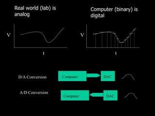
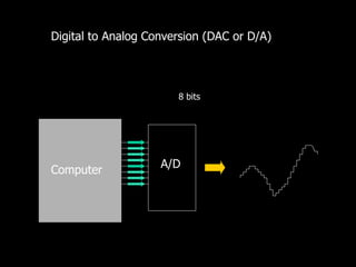
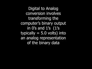
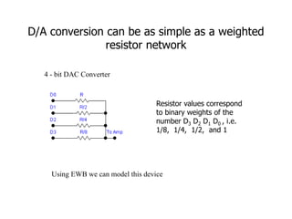
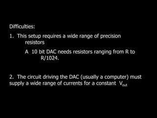
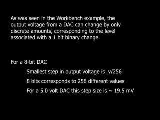
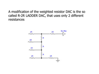
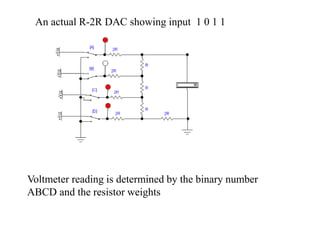
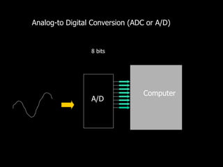
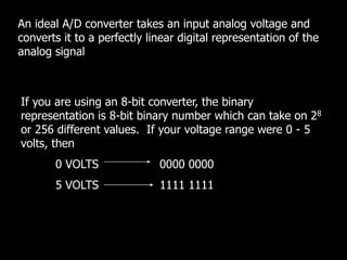
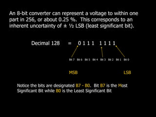
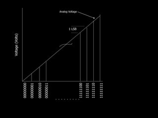
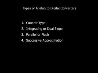
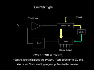
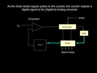
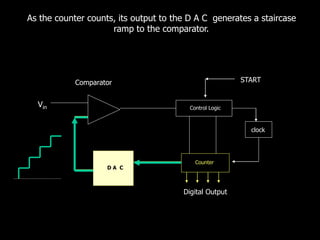
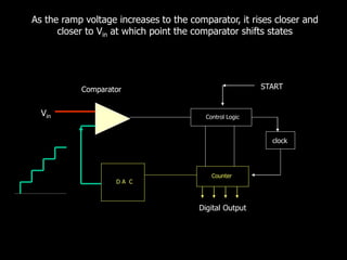
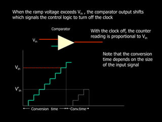
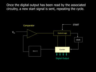
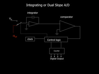
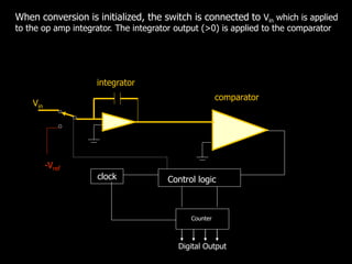
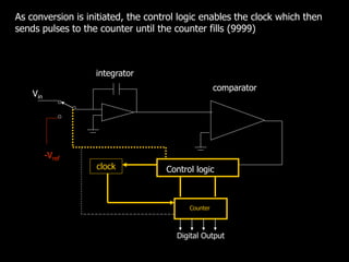
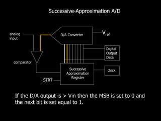
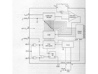
SlideShare a Scribd company logo
1 of 50
Digital to Analog and Analog
to Digital Conversion
D/A or DAC and
A/D or ADC
Real world (lab) is
analog
V
t t
Computer (binary) is
digital
D/A Conversion Computer DAC
DAC
A/D Conversion
V
Digital to Analog Conversion (DAC or D/A)
8 bits
Computer
A/D
Digital to Analog
conversion involves
transforming the
computer’s binary output
in 0’s and 1’s (1’s
typically = 5.0 volts) into
an analog representation
of the binary data
D/A conversion can be as simple as a weighted
resistor network
4 - bit DAC Converter
Resistor values correspond
to binary weights of the
number D3 D2 D1 D0 , i.e.
1/8, 1/4, 1/2, and 1
Using EWB we can model this device
Electronics Workbench Models
4bitDAC.ewb
Difficulties:
1. This setup requires a wide range of precision
resistors
A 10 bit DAC needs resistors ranging from R to
R/1024.
2. The circuit driving the DAC (usually a computer) must
supply a wide range of currents for a constant Vout
For a 8-bit DAC
Smallest step in output voltage is v/256
8 bits corresponds to 256 different values
For a 5.0 volt DAC this step size is ~ 19.5 mV
As was seen in the Workbench example, the
output voltage from a DAC can change by only
discrete amounts, corresponding to the level
associated with a 1 bit binary change.
A modification of the weighted resistor DAC is the so
called R-2R LADDER DAC, that uses only 2 different
resistances
An actual R-2R DAC showing input 1 0 1 1
Voltmeter reading is determined by the binary number
ABCD and the resistor weights
MSB = 1/2 of Vref
= 1/4 of Vref
= 1/8 of Vref
LSB = 1/16 of Vref
1 0 1 1 = 1/2 (5) + 1/4 (0) + 1/8 (5) + 1/16 (5)
 3.4 volts
In actual DACs, the converters will drive amplifier
circuits in most cases
R-2R Ladder DAC Workbench Model
Amplified DAC with bipolar ( ± Vout ) output
r2rdac.ewb
If one wants only positive or negative output, one can use a
BASELINE ADJ. for the Op Amp
baseline.ewb
Analog-to Digital Conversion (ADC or A/D)
A/D
8 bits
Computer
An ideal A/D converter takes an input analog voltage and
converts it to a perfectly linear digital representation of the
analog signal
If you are using an 8-bit converter, the binary
representation is 8-bit binary number which can take on 28
or 256 different values. If your voltage range were 0 - 5
volts, then
0 VOLTS 0000 0000
5 VOLTS 1111 1111
An 8-bit converter can represent a voltage to within one
part in 256, or about 0.25 %. This corresponds to an
inherent uncertainty of ± ½ LSB (least significant bit).
Decimal 128 = 0 1 1 1 1 1 1 1
Bit 1
Bit 2
Bit 3
Bit 4
Bit 5
Bit 6
Bit 7 Bit 0
LSB
MSB
Notice the bits are designated B7 - B0. Bit B7 is the Most
Significant Bit while B0 is the Least Significant Bit
00000000
00000001
00000010
00000011
11111111
11111110
11111101
. . . . . . . . .
Voltage
(Volts)
Analog Voltage
11111100
1 LSB
Number of Bits (N) Resolution (1/2N) Increment (mV) for 5 volts
6 1/64 78.1
8 1/256 19.6
10 1/1024 4.9
12 1/4096 1.2
14 1/16384 0.3
16 1/65536 0.07
Types of Analog to Digital Converters
1. Counter Type
2. Integrating or Dual Slope
3. Parallel or Flash
4. Successive Approximation
Counter Type
Control Logic
D A C
Counter
START
Vin
Comparator
Digital Output
clock
•When START is received,
•control logic initializes the system, (sets counter to 0), and
•turns on Clock sending regular pulses to the counter.
As the Clock sends regular pulses to the counter, the counter outputs a
digital signal to the Digital-to-Analog converter
D A C
Counter
START
Vin
Comparator
Digital Output
clock
Control Logic
Control Logic
D A C
Counter
START
Vin
Comparator
Digital Output
clock
As the counter counts, its output to the D A C generates a staircase
ramp to the comparator.
Control Logic
D A C
Counter
START
Vin
Comparator
Digital Output
clock
As the ramp voltage increases to the comparator, it rises closer and
closer to Vin at which point the comparator shifts states
When the ramp voltage exceeds Vin , the comparator output shifts
which signals the control logic to turn off the clock
Vin
Conversion time
V’in
Conv.time
With the clock off, the counter
reading is proportional to Vin
Note that the conversion
time depends on the size
of the input signal
Vin
Comparator
Control Logic
D A C
Counter
START
Vin
Comparator
Digital Output
clock
Once the digital output has been read by the associated
circuitry, a new start signal is sent, repeating the cycle.
With a counter type A/D, if the signal is varying
rapidly, the counter must count up and reset before
each cycle can begin, making it difficult to follow the
signal.
Track & Hold Logic
D A C
Up/Down
Counter
Vin
Comparator
Digital Output
clock
Tracking ADC - similar to the counter type except it uses an
up/down counter and can track a varying signal more quickly
Vin
-Vref
Control logic
Counter
clock
comparator
integrator
Digital Output
Integrating or Dual Slope A/D
Vin
-Vref
Control logic
Counter
clock
comparator
integrator
Digital Output
When conversion is initialized, the switch is connected to Vin which is applied
to the op amp integrator. The integrator output (>0) is applied to the comparator
Vin
-Vref
Control logic
Counter
clock
comparator
integrator
Digital Output
As conversion is initiated, the control logic enables the clock which then
sends pulses to the counter until the counter fills (9999)
Vin
-Vref
Control logic
Counter
clock
comparator
integrator
Digital Output
overflow
As the counter resets (9999  0000), an overflow signal is sent to the
control logic
this activates the input switch from Vin to
-Vref , applying a negative reference voltage to
the integrator
The negative reference voltage removes the charge stored
in the integrator until the charge becomes zero.
The total number of counts on the counter (determined by
the time it took the fixed voltage Vref to cancel Vin ) is
proportional to the input voltage, and thus is a measure of
the unknown input voltage.
At this point, the comparator switches states producing a
signal that disables the clock and freezes the counter
reading.
fixed time
measured time
Integrator
Output
Voltage
full scale conversion
quarter scale conversion
half scale conversion
The operation of this A/D requires 2 voltage slopes,
hence the common name DUAL-SLOPE.
charging up
the capacitor discharging
the capacitor
Since this A/D integrates the input as part of the measuring
process, any random noise present in the signal will tend to
integrate to zero, resulting in a reduction in noise.
These type of A/D s are used in almost all digital meters.
Such meters usually are not used to read rapidly changing
values in the lab. Consequently the major disadvantage of
such converters (very low speeds) is not a problem when
the readout update rate is only a few times per second.
If very high speed conversions are needed, e.g. video
conversions, the most commonly used converter is a
Flash Converter.
While such converters are extremely fast, they are
also very costly compared to other types.
Flash Converters
Parallel or Flash Converters
The resistor network is a precision voltage divider, dividing
Vref (8 volts in the sample) into equal voltage increments
(1.0 volts here) to one input of the comparator. The other
comparator input is the input voltage
Each comparator switches immediately when Vin exceeds
Vref . Comparators whose input does not exceed Vref do not
switch.
A decoder circuit (a 74148 8-to-3 priority decoder here)
converts the comparator outputs to a useful output (here
binary)
The speed of the converter is limited only by the speeds of
the comparators and the logic network. Speeds in excess of
20 to 30 MHz are common, and speeds > 100 MHz are
available ($$$$$).
The cost stems from the circuit complexity since the number
of comparators and resistors required increases rapidly. The 3-
bit example required 7 converters, 6-bits would require 63,
while an 8-bits converter would need 256 comparators and
equivalent precision resistors.
While integrating or dual-slope A/Ds are widely used in
digital instruments such as DVMs, the most common
A/D used in the laboratory environment is the successive
approximation.
Successive approximation converters are reasonably
priced for large bit values, i.e. 10, 12 and even 16 bit
converters can be obtained for well under $100. Their
conversion times, typically ~ 10-20 s, are adequate for
most laboratory functions.
Successive-Approximation A/D
Successive
Approximation
Register
D/A Converter Vref
clock
analog
input
Digital
Output
Data
At initialization, all bits from the SAR are set to zero, and
conversion begins by taking STRT line low.
comparator
STRT
Successive
Approximation
Register
D/A Converter Vref
clock
analog
input
Digital
Output
Data
comparator
STRT
Successive-Approximation A/D
First the logic in the SAR sets the MSB bit equal to
1 (+5 V). Remember that a 1 in bit 7 will be half of
full scale.
Successive
Approximation
Register
D/A Converter Vref
clock
analog
input
Digital
Output
Data
comparator
STRT
Successive-Approximation A/D
The output of the SAR feeds the D/A converter
producing an output compared to the analog input
voltage. If the D/A output is < Vin then the MSB is left
at 1 and the next bit is then tested.
Successive
Approximation
Register
D/A Converter Vref
clock
analog
input
Digital
Output
Data
comparator
STRT
Successive-Approximation A/D
If the D/A output is > Vin then the MSB is set to 0 and
the next bit is set equal to 1.
Successive bits are set and tested by comparing the DAC
output to the input Vin in an 8 step process (for an 8-bit
converter) that results in a valid 8-bit binary output that
represents the input voltage.
CLOCK PERIOD
¼FS
½FS
¾FS
1 2 3 4 5 6 7 8
analog input voltage
D/A output for 8-bit
conversion with output
code 1011 0111
Successive approximation search tree
for a 4-bit A/D
1111
1110
1101
1100
1011
1010
1001
1000
0111
0110
0101
0100
0011
0010
0001
D/A output
compared with
Vin to see if
larger or smaller
Note that the successive approximation process takes
a fixed time - 8 clock cycles for the 8-bit example.
For greater accuracy, one must use a higher bit
converter, i.e. 10-bit, 12-bit, etc. However, the depth
of the search and the time required increases with the
bit count.
dac_dig.ewb
flash adc(works).ewb
Workbench Models
adc-dac2.ewb

More Related Content

Similar to digital anlage c converter for digital .ppt

Similar to digital anlage c converter for digital .ppt (20)

Prese000
Prese000Prese000
Prese000
 
Pic ppt 13104022(4th_year)
Pic ppt 13104022(4th_year)Pic ppt 13104022(4th_year)
Pic ppt 13104022(4th_year)
 
Data convertors
Data convertorsData convertors
Data convertors
 
Analog to digital converter
Analog to digital converterAnalog to digital converter
Analog to digital converter
 
Adc.pptx ashvani 151503
Adc.pptx ashvani 151503Adc.pptx ashvani 151503
Adc.pptx ashvani 151503
 
ADC and DAC Best Ever Pers
ADC and DAC Best Ever PersADC and DAC Best Ever Pers
ADC and DAC Best Ever Pers
 
adcanddac hai kya bhayy me know if-01.pptx
adcanddac hai kya bhayy me know if-01.pptxadcanddac hai kya bhayy me know if-01.pptx
adcanddac hai kya bhayy me know if-01.pptx
 
Adc by anil kr yadav
Adc by anil kr yadavAdc by anil kr yadav
Adc by anil kr yadav
 
Analog to digital converter
Analog to digital converterAnalog to digital converter
Analog to digital converter
 
Adc f05
Adc f05Adc f05
Adc f05
 
Adc and dac
Adc and dacAdc and dac
Adc and dac
 
UNIT 4 & 5 - I nterfacing_Lecture7.pptx
UNIT 4 & 5 - I         nterfacing_Lecture7.pptxUNIT 4 & 5 - I         nterfacing_Lecture7.pptx
UNIT 4 & 5 - I nterfacing_Lecture7.pptx
 
analog to digital converter.ppt
analog to digital converter.pptanalog to digital converter.ppt
analog to digital converter.ppt
 
05 analog control_sp15
05 analog control_sp1505 analog control_sp15
05 analog control_sp15
 
Analog to Digital Conversion
Analog to Digital ConversionAnalog to Digital Conversion
Analog to Digital Conversion
 
ADC & DAC
ADC & DAC ADC & DAC
ADC & DAC
 
Meeting w9 chapter 3 part 2
Meeting w9   chapter 3 part 2Meeting w9   chapter 3 part 2
Meeting w9 chapter 3 part 2
 
Lica 7th chapter slides
Lica 7th chapter slidesLica 7th chapter slides
Lica 7th chapter slides
 
5942709.ppt
5942709.ppt5942709.ppt
5942709.ppt
 
MODULE-2_SIGNAL_CONDITIONING.pptx
MODULE-2_SIGNAL_CONDITIONING.pptxMODULE-2_SIGNAL_CONDITIONING.pptx
MODULE-2_SIGNAL_CONDITIONING.pptx
 

More from AbdullahOmar64

More from AbdullahOmar64 (14)

LineCoding_ADCS.ppt
LineCoding_ADCS.pptLineCoding_ADCS.ppt
LineCoding_ADCS.ppt
 
companding.ppt
companding.pptcompanding.ppt
companding.ppt
 
The_Role_of_Raised_Cosine.pdf
The_Role_of_Raised_Cosine.pdfThe_Role_of_Raised_Cosine.pdf
The_Role_of_Raised_Cosine.pdf
 
09-SpreadSpectrum.ppt
09-SpreadSpectrum.ppt09-SpreadSpectrum.ppt
09-SpreadSpectrum.ppt
 
3-Matched-Filter.ppt
3-Matched-Filter.ppt3-Matched-Filter.ppt
3-Matched-Filter.ppt
 
mod.pptx
mod.pptxmod.pptx
mod.pptx
 
waveforms.ppt
waveforms.pptwaveforms.ppt
waveforms.ppt
 
aliasing.ppt
aliasing.pptaliasing.ppt
aliasing.ppt
 
Lecture_4_Data_Gathering_and_Analysis.pdf
Lecture_4_Data_Gathering_and_Analysis.pdfLecture_4_Data_Gathering_and_Analysis.pdf
Lecture_4_Data_Gathering_and_Analysis.pdf
 
INI_800_Lecture_1_Introduction.pdf
INI_800_Lecture_1_Introduction.pdfINI_800_Lecture_1_Introduction.pdf
INI_800_Lecture_1_Introduction.pdf
 
books-library.online-02011910Vr3Z0.pdf
books-library.online-02011910Vr3Z0.pdfbooks-library.online-02011910Vr3Z0.pdf
books-library.online-02011910Vr3Z0.pdf
 
نظم-العد.pdf
نظم-العد.pdfنظم-العد.pdf
نظم-العد.pdf
 
convert number.pdf
convert number.pdfconvert number.pdf
convert number.pdf
 
Guide latex.
Guide latex.Guide latex.
Guide latex.
 

Recently uploaded

Coefficient of Thermal Expansion and their Importance.pptx
Coefficient of Thermal Expansion and their Importance.pptxCoefficient of Thermal Expansion and their Importance.pptx
Coefficient of Thermal Expansion and their Importance.pptxAsutosh Ranjan
 
High Profile Call Girls Nashik Megha 7001305949 Independent Escort Service Na...
High Profile Call Girls Nashik Megha 7001305949 Independent Escort Service Na...High Profile Call Girls Nashik Megha 7001305949 Independent Escort Service Na...
High Profile Call Girls Nashik Megha 7001305949 Independent Escort Service Na...Call Girls in Nagpur High Profile
 
Model Call Girl in Narela Delhi reach out to us at 🔝8264348440🔝
Model Call Girl in Narela Delhi reach out to us at 🔝8264348440🔝Model Call Girl in Narela Delhi reach out to us at 🔝8264348440🔝
Model Call Girl in Narela Delhi reach out to us at 🔝8264348440🔝soniya singh
 
(PRIYA) Rajgurunagar Call Girls Just Call 7001035870 [ Cash on Delivery ] Pun...
(PRIYA) Rajgurunagar Call Girls Just Call 7001035870 [ Cash on Delivery ] Pun...(PRIYA) Rajgurunagar Call Girls Just Call 7001035870 [ Cash on Delivery ] Pun...
(PRIYA) Rajgurunagar Call Girls Just Call 7001035870 [ Cash on Delivery ] Pun...ranjana rawat
 
IVE Industry Focused Event - Defence Sector 2024
IVE Industry Focused Event - Defence Sector 2024IVE Industry Focused Event - Defence Sector 2024
IVE Industry Focused Event - Defence Sector 2024Mark Billinghurst
 
MANUFACTURING PROCESS-II UNIT-5 NC MACHINE TOOLS
MANUFACTURING PROCESS-II UNIT-5 NC MACHINE TOOLSMANUFACTURING PROCESS-II UNIT-5 NC MACHINE TOOLS
MANUFACTURING PROCESS-II UNIT-5 NC MACHINE TOOLSSIVASHANKAR N
 
(ANVI) Koregaon Park Call Girls Just Call 7001035870 [ Cash on Delivery ] Pun...
(ANVI) Koregaon Park Call Girls Just Call 7001035870 [ Cash on Delivery ] Pun...(ANVI) Koregaon Park Call Girls Just Call 7001035870 [ Cash on Delivery ] Pun...
(ANVI) Koregaon Park Call Girls Just Call 7001035870 [ Cash on Delivery ] Pun...ranjana rawat
 
High Profile Call Girls Nagpur Meera Call 7001035870 Meet With Nagpur Escorts
High Profile Call Girls Nagpur Meera Call 7001035870 Meet With Nagpur EscortsHigh Profile Call Girls Nagpur Meera Call 7001035870 Meet With Nagpur Escorts
High Profile Call Girls Nagpur Meera Call 7001035870 Meet With Nagpur EscortsCall Girls in Nagpur High Profile
 
(MEERA) Dapodi Call Girls Just Call 7001035870 [ Cash on Delivery ] Pune Escorts
(MEERA) Dapodi Call Girls Just Call 7001035870 [ Cash on Delivery ] Pune Escorts(MEERA) Dapodi Call Girls Just Call 7001035870 [ Cash on Delivery ] Pune Escorts
(MEERA) Dapodi Call Girls Just Call 7001035870 [ Cash on Delivery ] Pune Escortsranjana rawat
 
Microscopic Analysis of Ceramic Materials.pptx
Microscopic Analysis of Ceramic Materials.pptxMicroscopic Analysis of Ceramic Materials.pptx
Microscopic Analysis of Ceramic Materials.pptxpurnimasatapathy1234
 
VIP Call Girls Service Hitech City Hyderabad Call +91-8250192130
VIP Call Girls Service Hitech City Hyderabad Call +91-8250192130VIP Call Girls Service Hitech City Hyderabad Call +91-8250192130
VIP Call Girls Service Hitech City Hyderabad Call +91-8250192130Suhani Kapoor
 
Architect Hassan Khalil Portfolio for 2024
Architect Hassan Khalil Portfolio for 2024Architect Hassan Khalil Portfolio for 2024
Architect Hassan Khalil Portfolio for 2024hassan khalil
 
Study on Air-Water & Water-Water Heat Exchange in a Finned Tube Exchanger
Study on Air-Water & Water-Water Heat Exchange in a Finned Tube ExchangerStudy on Air-Water & Water-Water Heat Exchange in a Finned Tube Exchanger
Study on Air-Water & Water-Water Heat Exchange in a Finned Tube ExchangerAnamika Sarkar
 
HARMONY IN THE NATURE AND EXISTENCE - Unit-IV
HARMONY IN THE NATURE AND EXISTENCE - Unit-IVHARMONY IN THE NATURE AND EXISTENCE - Unit-IV
HARMONY IN THE NATURE AND EXISTENCE - Unit-IVRajaP95
 
SPICE PARK APR2024 ( 6,793 SPICE Models )
SPICE PARK APR2024 ( 6,793 SPICE Models )SPICE PARK APR2024 ( 6,793 SPICE Models )
SPICE PARK APR2024 ( 6,793 SPICE Models )Tsuyoshi Horigome
 
(RIA) Call Girls Bhosari ( 7001035870 ) HI-Fi Pune Escorts Service
(RIA) Call Girls Bhosari ( 7001035870 ) HI-Fi Pune Escorts Service(RIA) Call Girls Bhosari ( 7001035870 ) HI-Fi Pune Escorts Service
(RIA) Call Girls Bhosari ( 7001035870 ) HI-Fi Pune Escorts Serviceranjana rawat
 
GDSC ASEB Gen AI study jams presentation
GDSC ASEB Gen AI study jams presentationGDSC ASEB Gen AI study jams presentation
GDSC ASEB Gen AI study jams presentationGDSCAESB
 

Recently uploaded (20)

Coefficient of Thermal Expansion and their Importance.pptx
Coefficient of Thermal Expansion and their Importance.pptxCoefficient of Thermal Expansion and their Importance.pptx
Coefficient of Thermal Expansion and their Importance.pptx
 
High Profile Call Girls Nashik Megha 7001305949 Independent Escort Service Na...
High Profile Call Girls Nashik Megha 7001305949 Independent Escort Service Na...High Profile Call Girls Nashik Megha 7001305949 Independent Escort Service Na...
High Profile Call Girls Nashik Megha 7001305949 Independent Escort Service Na...
 
Model Call Girl in Narela Delhi reach out to us at 🔝8264348440🔝
Model Call Girl in Narela Delhi reach out to us at 🔝8264348440🔝Model Call Girl in Narela Delhi reach out to us at 🔝8264348440🔝
Model Call Girl in Narela Delhi reach out to us at 🔝8264348440🔝
 
(PRIYA) Rajgurunagar Call Girls Just Call 7001035870 [ Cash on Delivery ] Pun...
(PRIYA) Rajgurunagar Call Girls Just Call 7001035870 [ Cash on Delivery ] Pun...(PRIYA) Rajgurunagar Call Girls Just Call 7001035870 [ Cash on Delivery ] Pun...
(PRIYA) Rajgurunagar Call Girls Just Call 7001035870 [ Cash on Delivery ] Pun...
 
IVE Industry Focused Event - Defence Sector 2024
IVE Industry Focused Event - Defence Sector 2024IVE Industry Focused Event - Defence Sector 2024
IVE Industry Focused Event - Defence Sector 2024
 
MANUFACTURING PROCESS-II UNIT-5 NC MACHINE TOOLS
MANUFACTURING PROCESS-II UNIT-5 NC MACHINE TOOLSMANUFACTURING PROCESS-II UNIT-5 NC MACHINE TOOLS
MANUFACTURING PROCESS-II UNIT-5 NC MACHINE TOOLS
 
9953056974 Call Girls In South Ex, Escorts (Delhi) NCR.pdf
9953056974 Call Girls In South Ex, Escorts (Delhi) NCR.pdf9953056974 Call Girls In South Ex, Escorts (Delhi) NCR.pdf
9953056974 Call Girls In South Ex, Escorts (Delhi) NCR.pdf
 
(ANVI) Koregaon Park Call Girls Just Call 7001035870 [ Cash on Delivery ] Pun...
(ANVI) Koregaon Park Call Girls Just Call 7001035870 [ Cash on Delivery ] Pun...(ANVI) Koregaon Park Call Girls Just Call 7001035870 [ Cash on Delivery ] Pun...
(ANVI) Koregaon Park Call Girls Just Call 7001035870 [ Cash on Delivery ] Pun...
 
★ CALL US 9953330565 ( HOT Young Call Girls In Badarpur delhi NCR
★ CALL US 9953330565 ( HOT Young Call Girls In Badarpur delhi NCR★ CALL US 9953330565 ( HOT Young Call Girls In Badarpur delhi NCR
★ CALL US 9953330565 ( HOT Young Call Girls In Badarpur delhi NCR
 
High Profile Call Girls Nagpur Meera Call 7001035870 Meet With Nagpur Escorts
High Profile Call Girls Nagpur Meera Call 7001035870 Meet With Nagpur EscortsHigh Profile Call Girls Nagpur Meera Call 7001035870 Meet With Nagpur Escorts
High Profile Call Girls Nagpur Meera Call 7001035870 Meet With Nagpur Escorts
 
(MEERA) Dapodi Call Girls Just Call 7001035870 [ Cash on Delivery ] Pune Escorts
(MEERA) Dapodi Call Girls Just Call 7001035870 [ Cash on Delivery ] Pune Escorts(MEERA) Dapodi Call Girls Just Call 7001035870 [ Cash on Delivery ] Pune Escorts
(MEERA) Dapodi Call Girls Just Call 7001035870 [ Cash on Delivery ] Pune Escorts
 
Microscopic Analysis of Ceramic Materials.pptx
Microscopic Analysis of Ceramic Materials.pptxMicroscopic Analysis of Ceramic Materials.pptx
Microscopic Analysis of Ceramic Materials.pptx
 
VIP Call Girls Service Hitech City Hyderabad Call +91-8250192130
VIP Call Girls Service Hitech City Hyderabad Call +91-8250192130VIP Call Girls Service Hitech City Hyderabad Call +91-8250192130
VIP Call Girls Service Hitech City Hyderabad Call +91-8250192130
 
Architect Hassan Khalil Portfolio for 2024
Architect Hassan Khalil Portfolio for 2024Architect Hassan Khalil Portfolio for 2024
Architect Hassan Khalil Portfolio for 2024
 
Study on Air-Water & Water-Water Heat Exchange in a Finned Tube Exchanger
Study on Air-Water & Water-Water Heat Exchange in a Finned Tube ExchangerStudy on Air-Water & Water-Water Heat Exchange in a Finned Tube Exchanger
Study on Air-Water & Water-Water Heat Exchange in a Finned Tube Exchanger
 
Call Us -/9953056974- Call Girls In Vikaspuri-/- Delhi NCR
Call Us -/9953056974- Call Girls In Vikaspuri-/- Delhi NCRCall Us -/9953056974- Call Girls In Vikaspuri-/- Delhi NCR
Call Us -/9953056974- Call Girls In Vikaspuri-/- Delhi NCR
 
HARMONY IN THE NATURE AND EXISTENCE - Unit-IV
HARMONY IN THE NATURE AND EXISTENCE - Unit-IVHARMONY IN THE NATURE AND EXISTENCE - Unit-IV
HARMONY IN THE NATURE AND EXISTENCE - Unit-IV
 
SPICE PARK APR2024 ( 6,793 SPICE Models )
SPICE PARK APR2024 ( 6,793 SPICE Models )SPICE PARK APR2024 ( 6,793 SPICE Models )
SPICE PARK APR2024 ( 6,793 SPICE Models )
 
(RIA) Call Girls Bhosari ( 7001035870 ) HI-Fi Pune Escorts Service
(RIA) Call Girls Bhosari ( 7001035870 ) HI-Fi Pune Escorts Service(RIA) Call Girls Bhosari ( 7001035870 ) HI-Fi Pune Escorts Service
(RIA) Call Girls Bhosari ( 7001035870 ) HI-Fi Pune Escorts Service
 
GDSC ASEB Gen AI study jams presentation
GDSC ASEB Gen AI study jams presentationGDSC ASEB Gen AI study jams presentation
GDSC ASEB Gen AI study jams presentation
 

digital anlage c converter for digital .ppt

  • 1. Digital to Analog and Analog to Digital Conversion D/A or DAC and A/D or ADC
  • 2. Real world (lab) is analog V t t Computer (binary) is digital D/A Conversion Computer DAC DAC A/D Conversion V
  • 3. Digital to Analog Conversion (DAC or D/A) 8 bits Computer A/D
  • 4. Digital to Analog conversion involves transforming the computer’s binary output in 0’s and 1’s (1’s typically = 5.0 volts) into an analog representation of the binary data
  • 5. D/A conversion can be as simple as a weighted resistor network 4 - bit DAC Converter Resistor values correspond to binary weights of the number D3 D2 D1 D0 , i.e. 1/8, 1/4, 1/2, and 1 Using EWB we can model this device
  • 7. Difficulties: 1. This setup requires a wide range of precision resistors A 10 bit DAC needs resistors ranging from R to R/1024. 2. The circuit driving the DAC (usually a computer) must supply a wide range of currents for a constant Vout
  • 8. For a 8-bit DAC Smallest step in output voltage is v/256 8 bits corresponds to 256 different values For a 5.0 volt DAC this step size is ~ 19.5 mV As was seen in the Workbench example, the output voltage from a DAC can change by only discrete amounts, corresponding to the level associated with a 1 bit binary change.
  • 9. A modification of the weighted resistor DAC is the so called R-2R LADDER DAC, that uses only 2 different resistances
  • 10. An actual R-2R DAC showing input 1 0 1 1 Voltmeter reading is determined by the binary number ABCD and the resistor weights
  • 11. MSB = 1/2 of Vref = 1/4 of Vref = 1/8 of Vref LSB = 1/16 of Vref 1 0 1 1 = 1/2 (5) + 1/4 (0) + 1/8 (5) + 1/16 (5)  3.4 volts In actual DACs, the converters will drive amplifier circuits in most cases
  • 12. R-2R Ladder DAC Workbench Model
  • 13. Amplified DAC with bipolar ( ± Vout ) output r2rdac.ewb
  • 14. If one wants only positive or negative output, one can use a BASELINE ADJ. for the Op Amp baseline.ewb
  • 15. Analog-to Digital Conversion (ADC or A/D) A/D 8 bits Computer
  • 16. An ideal A/D converter takes an input analog voltage and converts it to a perfectly linear digital representation of the analog signal If you are using an 8-bit converter, the binary representation is 8-bit binary number which can take on 28 or 256 different values. If your voltage range were 0 - 5 volts, then 0 VOLTS 0000 0000 5 VOLTS 1111 1111
  • 17. An 8-bit converter can represent a voltage to within one part in 256, or about 0.25 %. This corresponds to an inherent uncertainty of ± ½ LSB (least significant bit). Decimal 128 = 0 1 1 1 1 1 1 1 Bit 1 Bit 2 Bit 3 Bit 4 Bit 5 Bit 6 Bit 7 Bit 0 LSB MSB Notice the bits are designated B7 - B0. Bit B7 is the Most Significant Bit while B0 is the Least Significant Bit
  • 18. 00000000 00000001 00000010 00000011 11111111 11111110 11111101 . . . . . . . . . Voltage (Volts) Analog Voltage 11111100 1 LSB
  • 19. Number of Bits (N) Resolution (1/2N) Increment (mV) for 5 volts 6 1/64 78.1 8 1/256 19.6 10 1/1024 4.9 12 1/4096 1.2 14 1/16384 0.3 16 1/65536 0.07
  • 20. Types of Analog to Digital Converters 1. Counter Type 2. Integrating or Dual Slope 3. Parallel or Flash 4. Successive Approximation
  • 21. Counter Type Control Logic D A C Counter START Vin Comparator Digital Output clock •When START is received, •control logic initializes the system, (sets counter to 0), and •turns on Clock sending regular pulses to the counter.
  • 22. As the Clock sends regular pulses to the counter, the counter outputs a digital signal to the Digital-to-Analog converter D A C Counter START Vin Comparator Digital Output clock Control Logic
  • 23. Control Logic D A C Counter START Vin Comparator Digital Output clock As the counter counts, its output to the D A C generates a staircase ramp to the comparator.
  • 24. Control Logic D A C Counter START Vin Comparator Digital Output clock As the ramp voltage increases to the comparator, it rises closer and closer to Vin at which point the comparator shifts states
  • 25. When the ramp voltage exceeds Vin , the comparator output shifts which signals the control logic to turn off the clock Vin Conversion time V’in Conv.time With the clock off, the counter reading is proportional to Vin Note that the conversion time depends on the size of the input signal Vin Comparator
  • 26. Control Logic D A C Counter START Vin Comparator Digital Output clock Once the digital output has been read by the associated circuitry, a new start signal is sent, repeating the cycle.
  • 27. With a counter type A/D, if the signal is varying rapidly, the counter must count up and reset before each cycle can begin, making it difficult to follow the signal.
  • 28. Track & Hold Logic D A C Up/Down Counter Vin Comparator Digital Output clock Tracking ADC - similar to the counter type except it uses an up/down counter and can track a varying signal more quickly
  • 30. Vin -Vref Control logic Counter clock comparator integrator Digital Output When conversion is initialized, the switch is connected to Vin which is applied to the op amp integrator. The integrator output (>0) is applied to the comparator
  • 31. Vin -Vref Control logic Counter clock comparator integrator Digital Output As conversion is initiated, the control logic enables the clock which then sends pulses to the counter until the counter fills (9999)
  • 32. Vin -Vref Control logic Counter clock comparator integrator Digital Output overflow As the counter resets (9999  0000), an overflow signal is sent to the control logic this activates the input switch from Vin to -Vref , applying a negative reference voltage to the integrator
  • 33. The negative reference voltage removes the charge stored in the integrator until the charge becomes zero. The total number of counts on the counter (determined by the time it took the fixed voltage Vref to cancel Vin ) is proportional to the input voltage, and thus is a measure of the unknown input voltage. At this point, the comparator switches states producing a signal that disables the clock and freezes the counter reading.
  • 34. fixed time measured time Integrator Output Voltage full scale conversion quarter scale conversion half scale conversion The operation of this A/D requires 2 voltage slopes, hence the common name DUAL-SLOPE. charging up the capacitor discharging the capacitor
  • 35. Since this A/D integrates the input as part of the measuring process, any random noise present in the signal will tend to integrate to zero, resulting in a reduction in noise. These type of A/D s are used in almost all digital meters. Such meters usually are not used to read rapidly changing values in the lab. Consequently the major disadvantage of such converters (very low speeds) is not a problem when the readout update rate is only a few times per second.
  • 36. If very high speed conversions are needed, e.g. video conversions, the most commonly used converter is a Flash Converter. While such converters are extremely fast, they are also very costly compared to other types. Flash Converters
  • 37.
  • 38. Parallel or Flash Converters The resistor network is a precision voltage divider, dividing Vref (8 volts in the sample) into equal voltage increments (1.0 volts here) to one input of the comparator. The other comparator input is the input voltage Each comparator switches immediately when Vin exceeds Vref . Comparators whose input does not exceed Vref do not switch. A decoder circuit (a 74148 8-to-3 priority decoder here) converts the comparator outputs to a useful output (here binary)
  • 39. The speed of the converter is limited only by the speeds of the comparators and the logic network. Speeds in excess of 20 to 30 MHz are common, and speeds > 100 MHz are available ($$$$$). The cost stems from the circuit complexity since the number of comparators and resistors required increases rapidly. The 3- bit example required 7 converters, 6-bits would require 63, while an 8-bits converter would need 256 comparators and equivalent precision resistors.
  • 40. While integrating or dual-slope A/Ds are widely used in digital instruments such as DVMs, the most common A/D used in the laboratory environment is the successive approximation. Successive approximation converters are reasonably priced for large bit values, i.e. 10, 12 and even 16 bit converters can be obtained for well under $100. Their conversion times, typically ~ 10-20 s, are adequate for most laboratory functions.
  • 41. Successive-Approximation A/D Successive Approximation Register D/A Converter Vref clock analog input Digital Output Data At initialization, all bits from the SAR are set to zero, and conversion begins by taking STRT line low. comparator STRT
  • 42. Successive Approximation Register D/A Converter Vref clock analog input Digital Output Data comparator STRT Successive-Approximation A/D First the logic in the SAR sets the MSB bit equal to 1 (+5 V). Remember that a 1 in bit 7 will be half of full scale.
  • 43. Successive Approximation Register D/A Converter Vref clock analog input Digital Output Data comparator STRT Successive-Approximation A/D The output of the SAR feeds the D/A converter producing an output compared to the analog input voltage. If the D/A output is < Vin then the MSB is left at 1 and the next bit is then tested.
  • 44. Successive Approximation Register D/A Converter Vref clock analog input Digital Output Data comparator STRT Successive-Approximation A/D If the D/A output is > Vin then the MSB is set to 0 and the next bit is set equal to 1.
  • 45. Successive bits are set and tested by comparing the DAC output to the input Vin in an 8 step process (for an 8-bit converter) that results in a valid 8-bit binary output that represents the input voltage.
  • 46. CLOCK PERIOD ¼FS ½FS ¾FS 1 2 3 4 5 6 7 8 analog input voltage D/A output for 8-bit conversion with output code 1011 0111
  • 47. Successive approximation search tree for a 4-bit A/D 1111 1110 1101 1100 1011 1010 1001 1000 0111 0110 0101 0100 0011 0010 0001 D/A output compared with Vin to see if larger or smaller
  • 48. Note that the successive approximation process takes a fixed time - 8 clock cycles for the 8-bit example. For greater accuracy, one must use a higher bit converter, i.e. 10-bit, 12-bit, etc. However, the depth of the search and the time required increases with the bit count.
  • 49.