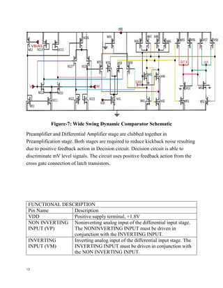
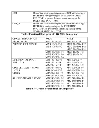
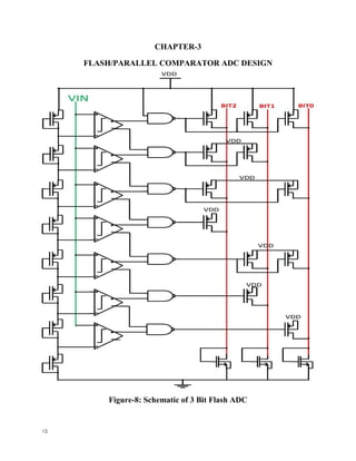
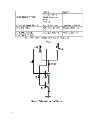
Downloaded 21 times
![8
(C) SIGMA DELTA ADC
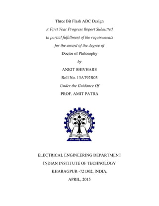
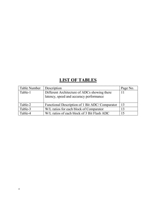
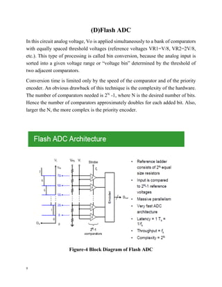
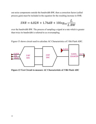
Here, the integrator is constantly ramping up or down at node A. The output of the
comparator is fed back through a 1-bit DAC to the summing input. The negative
feedback loop from the comparator output through the 1-bit DAC to the summing
point will force the average dc voltage at node B equal to VIN. This implies that
the average DAC output voltage must equal the input voltage VIN. The average
DAC output voltage is controlled by the ones-density in the 1-bit data stream from
the comparator output. If input signal increases towards +Vref, the number of
“ones” in the serial bit stream increases, and the number of “zeros” decreases.
Similarly, as the signal goes negative towards –Vref, the number of “ones” in the
serial bit stream decreases, and the number of “zeros” increases. Thus, it can be
shown that the average value of the input voltage is contained in the serial bit
stream out of the comparator. The digital filter and decimator process the serial bit
stream and produce the final output data. [3]
Figure-3 First-Order Sigma-Delta ADC](https://image.slidesharecdn.com/47fdd9a7-1204-49d6-bf1b-cb442a88e903-160313161149/85/3BITFLASHADC-8-320.jpg)
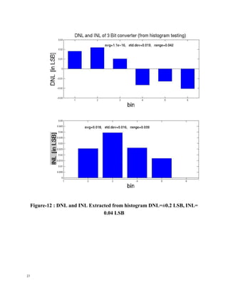
![19
transfer-function value the measured converter result is. It is defined as
follows-
𝐼𝑁𝐿(𝑛) =
𝑉𝑎𝑐𝑡𝑢𝑎𝑙(𝑛) − 𝑉𝑖𝑑𝑒𝑎𝑙(𝑛)
𝐿𝑆𝐵
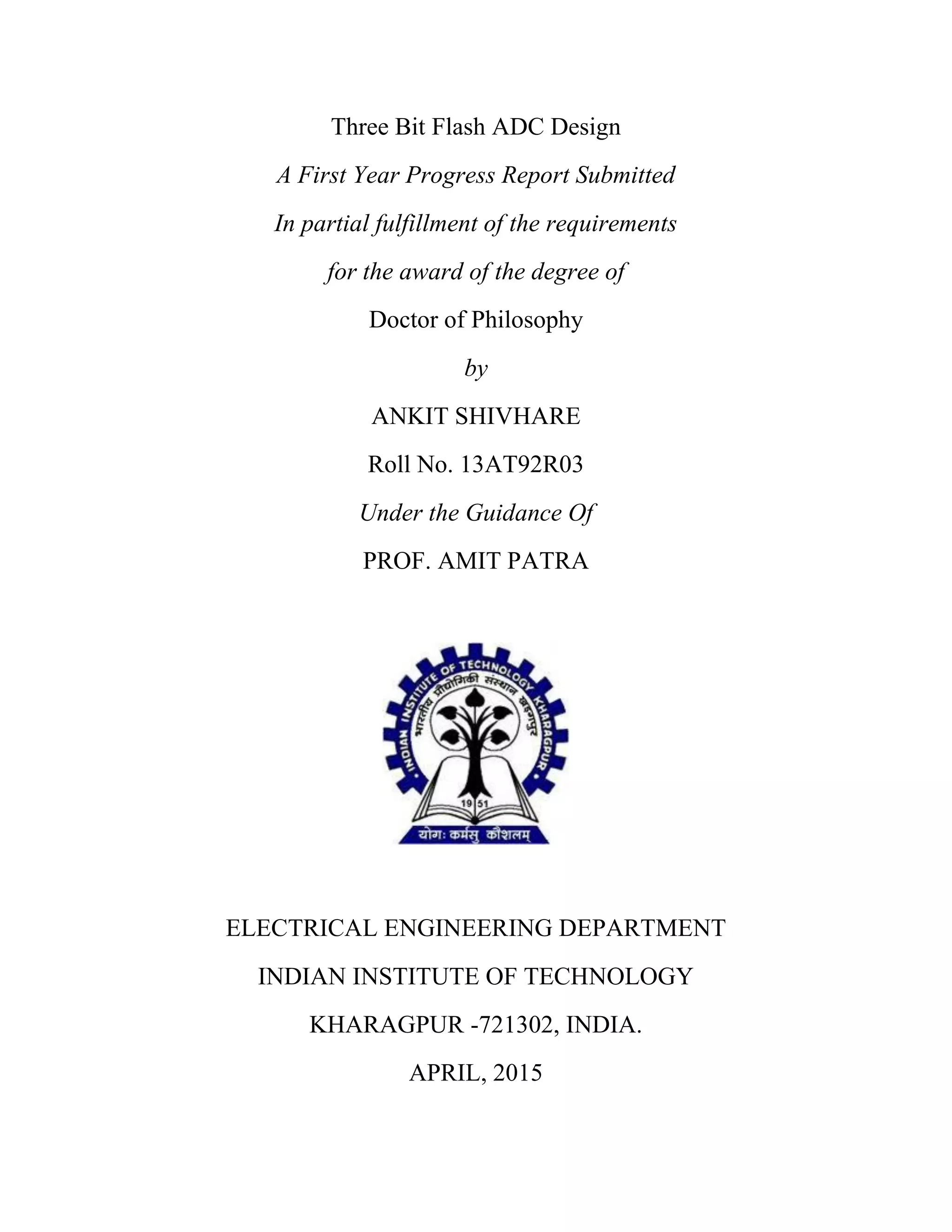
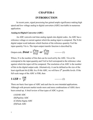
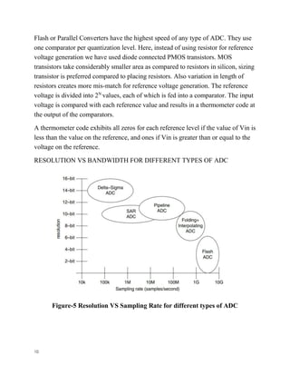
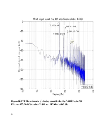
HISTOGRAM TESTING / CODE DENSITY TEST
The histogram test approach helps determine non linearity parameters such as
differential and integral nonlinearities (INL and DNL) in data converters. DNL is
derived directly from total occurrences of each code @ the output of the ADC [2].
ADC sampling rate, fs=100KHz, Ts=10µs, 1LSB= 10mV. For 0.01LSB
measurement resolution: n=100 samples/code. Thus, Ramp duration per
code:=100×10µsec=1msec. Ramp slope=10mV/msec.
Figure-11: Transient plot, Slow varying Ramp input is applied to meaasure
DC Characteristic of Flash ADC](https://image.slidesharecdn.com/47fdd9a7-1204-49d6-bf1b-cb442a88e903-160313161149/85/3BITFLASHADC-19-320.jpg)
![22
AC Performance
An ADC is defined by its bandwidth (the range of frequencies it can measure) and
its signal to noise ratio (how accurately it can measure a signal relative to the noise
it introduces). The actual bandwidth of an ADC is characterized primarily by its
sampling rate, and to a lesser extent by how it handles errors such as aliasing. The
dynamic range of an ADC is influenced by many factors, including the resolution
(the number of output levels it can quantize a signal to), linearity and accuracy
(how well the quantization levels match the true analog signal) and jitter (small
timing errors that introduce additional noise). The key specs to review are signal-
to-noise ratio (SNR), signal-to-noise and distortion ratio (SINAD), total harmonic
distortion (THD), and spurious-free dynamic range (SFDR). SINAD is defined as
the RMS value of an input sine wave to the RMS value of the noise of the
converter (from DC to the Nyquist frequency, including harmonic [total harmonic
distortion] content). Harmonic occurs at multiples of the input frequency. SNR is
similar to SINAD, except that it does not include the harmonic content. Thus, the
SNR should always be better than SINAD. Bot SNR and SINAD are typically
measured in dB.
SINAD = [6.02(N) +1.76] (dB) ------------------------------ (3)
Where, N is number of bits.
It equation (3) is rewritten in terms of N, it would reveal how many bits of
information are obtained as a function of the RMS noise:
N=(SINAD-1.76)/6.02 ------------------------------ (4)
Equation (4) is the definition of effective number of bits, or ENOB.
SINAD is a function of the input frequency. As frequency increases toward the
Nyquist limit, SINAD decreases. Thus, the performance will be much worse near
Nyquist frequency as compared to low frequencies.](https://image.slidesharecdn.com/47fdd9a7-1204-49d6-bf1b-cb442a88e903-160313161149/85/3BITFLASHADC-22-320.jpg)
![23
SNR is the signal-to-noise ratio with the distortion components removed. SNR
reveals where the noise floor of the converter is. One way to improve SNR is to
oversample, which provides a processing gain. Oversampling is a method of
lowering the noise floor of the converter by sampling at a rate much higher than
the signal of interest. This spreads the noise out over a wider range in the
frequency domain, thereby effectively reducing the noise at any one frequency bin.
A 2× oversampling reduces the noise floor by 3 dB. SNR can be computed using
𝑺𝑵𝑹 = [
𝑽𝒔𝒊𝒈𝒏𝒂𝒍, 𝒓𝒎𝒔
𝑽𝒏𝒐𝒊𝒔𝒆, 𝒓𝒎𝒔
] 𝒅𝑩
Spurious-Free Dynamic Range (SFDR) is defined as the ratio of the RMS
amplitude of the fundamental (maximum signal component) to the RMS value of
the next largest spurious component, excluding DC offset. It is typically expressed
in decibels relative to the carrier (dBc). SFDR is important in certain
communication applications that require maximizing the dynamic range of the
ADC. Spur prevent the ADC from converting small input signals, because the
distortion component can be much larger than the signal of interest. This limits the
dynamic range of the ADC. A large spur in the frequency domain in the frequency
domain may not significantly affect the SNR, but will significantly affect the
SFDR.
Total Harmonic Distortion (THD) measures the distortion content of a signal,
and is specified in decibels relative to the carrier (dBc). For ADCs, THD is the
ratio of the RMS sum of the selected harmonics of the input signal to the
fundamental itself. Only harmonics within the Nyquist limit are included in the
measurement.
𝑇𝐻𝐷 = 10log[
𝑉2
2
+ 𝑉3
2
+ ⋯ + 𝑉𝑛
2
𝑉1
2 ] 𝑑𝐵
In many applications, the actual signal of interest occupies a smaller bandwidth,
BW, which is less than the Nyquist bandwidth. If digital filtering is used to filter](https://image.slidesharecdn.com/47fdd9a7-1204-49d6-bf1b-cb442a88e903-160313161149/85/3BITFLASHADC-23-320.jpg)

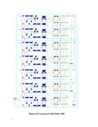
This document provides a summary of a progress report on the design of a 3-bit flash analog-to-digital converter (ADC). It describes the architecture and design of a comparator, which acts as a 1-bit ADC, and a 3-bit flash ADC. It also discusses characterization of the ADC's DC performance by measuring differential nonlinearity and integral nonlinearity from histograms. The document covers comparator design techniques, reference voltage generation using diode-connected transistors, and layout of the 3-bit flash ADC.


