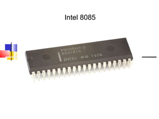
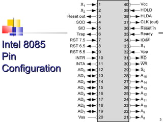
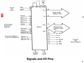
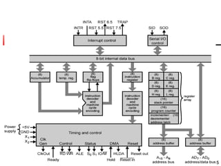
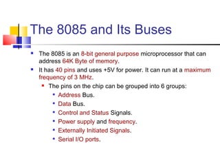
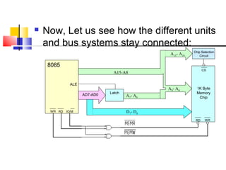
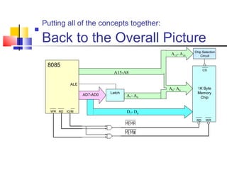
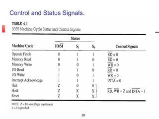
The document provides an introduction to the Intel 8085 microprocessor architecture. It discusses that the 8085 is an 8-bit processor that can address 64KB of memory using 40 pins running at a maximum of 3MHz. It describes the address bus, data bus, control signals, and CPU block diagram. It also explains the different types of machine cycles used by the 8085 like opcode fetch, memory read, and memory write and how instructions of different lengths require varying numbers of cycles.
BASIC INFORMATION OF ARCHITECTURE OF MICRO-CONTROLLER 8051 AS PER GTU SYLLABUS. Please Comment if u Like.. n Give u r feedback..
For More Information Go to
http://www.noesiseducation.blogspot.com
this is the brief description of the 8085 microprocessor. in this ppt, I described the key features of 8085, architecture, pin diagram, interfacing, timing diagram, some program, etc. I have also discussed the memory interfacing of 8085 microprocessor.
The word comes from the combination micro and processor.
Processor means a device that processes whatever. In this context processor means a device that processes numbers, specifically binary numbers, 0’s and 1’s.
To process means to manipulate. It is a general term that describes all manipulation. Again in this content, it means to perform certain operations on the numbers that depend on the microprocessor’s design.
It is a central processing unit etched on a single chip.A single integrated circuit has all the functional components of a cpu namely ALU,CONTROL UNIT & REGISTERS
8085 Pin Diagram, Demultiplexing and Generation Of Control Signals
Index::
Introduction of 8085 microprocessor
Logic pinout of 8085 microprocessor
Demultiplexing
Generation of control signals
Safalta Digital marketing institute in Noida, provide complete applications that encompass a huge range of virtual advertising and marketing additives, which includes search engine optimization, virtual communication advertising, pay-per-click on marketing, content material advertising, internet analytics, and greater. These university courses are designed for students who possess a comprehensive understanding of virtual marketing strategies and attributes.Safalta Digital Marketing Institute in Noida is a first choice for young individuals or students who are looking to start their careers in the field of digital advertising. The institute gives specialized courses designed and certification.
for beginners, providing thorough training in areas such as SEO, digital communication marketing, and PPC training in Noida. After finishing the program, students receive the certifications recognised by top different universitie, setting a strong foundation for a successful career in digital marketing.
Biological screening of herbal drugs: Introduction and Need for
Phyto-Pharmacological Screening, New Strategies for evaluating
Natural Products, In vitro evaluation techniques for Antioxidants, Antimicrobial and Anticancer drugs. In vivo evaluation techniques
for Anti-inflammatory, Antiulcer, Anticancer, Wound healing, Antidiabetic, Hepatoprotective, Cardio protective, Diuretics and
Antifertility, Toxicity studies as per OECD guidelines
June 3, 2024 Anti-Semitism Letter Sent to MIT President Kornbluth and MIT Cor...Levi Shapiro
Letter from the Congress of the United States regarding Anti-Semitism sent June 3rd to MIT President Sally Kornbluth, MIT Corp Chair, Mark Gorenberg
Dear Dr. Kornbluth and Mr. Gorenberg,
The US House of Representatives is deeply concerned by ongoing and pervasive acts of antisemitic
harassment and intimidation at the Massachusetts Institute of Technology (MIT). Failing to act decisively to ensure a safe learning environment for all students would be a grave dereliction of your responsibilities as President of MIT and Chair of the MIT Corporation.
This Congress will not stand idly by and allow an environment hostile to Jewish students to persist. The House believes that your institution is in violation of Title VI of the Civil Rights Act, and the inability or
unwillingness to rectify this violation through action requires accountability.
Postsecondary education is a unique opportunity for students to learn and have their ideas and beliefs challenged. However, universities receiving hundreds of millions of federal funds annually have denied
students that opportunity and have been hijacked to become venues for the promotion of terrorism, antisemitic harassment and intimidation, unlawful encampments, and in some cases, assaults and riots.
The House of Representatives will not countenance the use of federal funds to indoctrinate students into hateful, antisemitic, anti-American supporters of terrorism. Investigations into campus antisemitism by the Committee on Education and the Workforce and the Committee on Ways and Means have been expanded into a Congress-wide probe across all relevant jurisdictions to address this national crisis. The undersigned Committees will conduct oversight into the use of federal funds at MIT and its learning environment under authorities granted to each Committee.
• The Committee on Education and the Workforce has been investigating your institution since December 7, 2023. The Committee has broad jurisdiction over postsecondary education, including its compliance with Title VI of the Civil Rights Act, campus safety concerns over disruptions to the learning environment, and the awarding of federal student aid under the Higher Education Act.
• The Committee on Oversight and Accountability is investigating the sources of funding and other support flowing to groups espousing pro-Hamas propaganda and engaged in antisemitic harassment and intimidation of students. The Committee on Oversight and Accountability is the principal oversight committee of the US House of Representatives and has broad authority to investigate “any matter” at “any time” under House Rule X.
• The Committee on Ways and Means has been investigating several universities since November 15, 2023, when the Committee held a hearing entitled From Ivory Towers to Dark Corners: Investigating the Nexus Between Antisemitism, Tax-Exempt Universities, and Terror Financing. The Committee followed the hearing with letters to those institutions on January 10, 202
A workshop hosted by the South African Journal of Science aimed at postgraduate students and early career researchers with little or no experience in writing and publishing journal articles.
This presentation includes basic of PCOS their pathology and treatment and also Ayurveda correlation of PCOS and Ayurvedic line of treatment mentioned in classics.
2024.06.01 Introducing a competency framework for languag learning materials ...Sandy Millin
http://sandymillin.wordpress.com/iateflwebinar2024
Published classroom materials form the basis of syllabuses, drive teacher professional development, and have a potentially huge influence on learners, teachers and education systems. All teachers also create their own materials, whether a few sentences on a blackboard, a highly-structured fully-realised online course, or anything in between. Despite this, the knowledge and skills needed to create effective language learning materials are rarely part of teacher training, and are mostly learnt by trial and error.
Knowledge and skills frameworks, generally called competency frameworks, for ELT teachers, trainers and managers have existed for a few years now. However, until I created one for my MA dissertation, there wasn’t one drawing together what we need to know and do to be able to effectively produce language learning materials.
This webinar will introduce you to my framework, highlighting the key competencies I identified from my research. It will also show how anybody involved in language teaching (any language, not just English!), teacher training, managing schools or developing language learning materials can benefit from using the framework.
Read| The latest issue of The Challenger is here! We are thrilled to announce that our school paper has qualified for the NATIONAL SCHOOLS PRESS CONFERENCE (NSPC) 2024. Thank you for your unwavering support and trust. Dive into the stories that made us stand out!
1. An Introduction to
Microprocessor Architecture
using intel 8085 as a classic
processor
http://educate.intel.com/en/TheJourneyInside/ExploreTheCurriculum/EC_Microprocessors/
6. The 8085 and Its Buses
The 8085 is an 8-bit general purpose microprocessor that can
address 64K Byte of memory.
It has 40 pins and uses +5V for power. It can run at a maximum
frequency of 3 MHz.
The pins on the chip can be grouped into 6 groups:
Address Bus.
Data Bus.
Control and Status Signals.
Power supply and frequency.
Externally Initiated Signals.
Serial I/O ports.
7. The Address and Data Bus Systems
The address bus has 8 signal lines A8 – A15 which are
unidirectional.
The other 8 address bits are multiplexed (time shared) with the
8 data bits.
So, the bits AD0 – AD7 are bi-directional and serve as A0 –
A7 and D0 – D7 at the same time.
During the execution of the instruction, these lines carry
the address bits during the early part, then during the
late parts of the execution, they carry the 8 data bits.
In order to separate the address from the data, we can use a
latch to save the value before the function of the bits
changes.
9. The Control and Status
Signals
There are 4 main control and status signals. These are:
ALE: Address Latch Enable. This signal is a pulse that
become 1 when the AD0 – AD7 lines have an address
on them. It becomes 0 after that. This signal can be used
to enable a latch to save the address bits from the AD
lines.
RD: Read. Active low.
WR: Write. Active low.
IO/M: This signal specifies whether the operation is a
memory operation (IO/M=0) or an I/O operation
(IO/M=1).
S1 and S0 : Status signals to specify the kind of
operation being performed. Usually not used in small
systems.
10. Frequency Control Signals
There are 3 important pins in the frequency control group.
X0 and X1 are the inputs from the crystal or clock generating
circuit.
The frequency is internally divided by 2.
So, to run the microprocessor at 3 MHz, a clock
running at 6 MHz should be connected to the X0 and
X1 pins.
CLK (OUT): An output clock pin to drive the clock of the rest
of the system.
We will discuss the rest of the control signals as we get to them.
11. A closer look at the 8085
Architecture
Now, let’s look at some of its features
with more details.
12. The ALU
In addition to the arithmetic & logic circuits, the ALU
includes an accumulator, which is a part of every
arithmetic & logic operation.
Also, the ALU includes a temporary register used for
holding data temporarily during the execution of the
operation. This temporary register is not accessible
by the programmer.
13. The Flags register
There is also a flag register whose bits are affected by the arithmetic &
logic operations.
S-sign flag
The sign flag is set if bit D7 of the accumulator is set after an
arithmetic or logic operation.
Z-zero flag
Set if the result of the ALU operation is 0. Otherwise is reset.
This flag is affected by operations on the accumulator as well
as other registers. (DCR B).
AC-Auxiliary Carry
This flag is set when a carry is generated from bit D3 and
passed to D4 . This flag is used only internally for BCD
operations.
P-Parity flag
After an ALU operation, if the result has an even # of 1s, the
p-flag is set. Otherwise it is cleared. So, the flag can be used
to indicate even parity.
CY-carry flag
This flag is set when a carry is generated from bit D7 after an
unsigned operation.
OV-Overflow flag
This flag is set when an overflow occurs after a signed
operation.
14. Now, Let us see how the different units
and bus systems stay connected:
Chip Selection
A15- A10 Circuit
8085
CS
A15-A8
ALE
A9- A0 1K Byte
AD7-AD0 Latch Memory
A7- A0 Chip
WR RD IO/M D 7- D 0
RD WR
15. More on the 8085 machine
cycles
The 8085 executes several types of instructions
with each requiring a different number of
operations of different types. However, the
operations can be grouped into a small set.
The three main types are:
Memory Read and Write.
I/O Read and Write.
Request Acknowledge.
These can be further divided into various smaller
operations (machine cycles).
16. Opcode Fetch Machine Cycle
The first step of executing any instruction is the Opcode fetch
cycle.
In this cycle, the microprocessor brings in the instruction’s
Opcode from memory.
To differentiate this machine cycle from the very similar
“memory read” cycle, the control & status signals are set
as follows:
IO/M=0, s0 and s1 are both 1.
This machine cycle has four T-states.
The 8085 uses the first 3 T-states to fetch the opcode.
T4 is used to decode and execute it.
It is also possible for an instruction to have 6 T-states in an
opcode fetch machine cycle.
17. Memory Read Machine Cycle
The memory read machine cycle is
exactly the same as the opcode fetch
except:
It only has 3 T-states
The s0 signal is set to 0 instead.
18. The Memory Read Machine Cycle
To understand the memory read machine cycle, let’s
2000H 3E
study the execution of the following instruction:
2001H 32
MVI A, 32
In memory, this instruction looks like:
The first byte 3EH represents the opcode for loading
a byte into the accumulator (MVI A), the second byte
is the data to be loaded.
The 8085 needs to read these two bytes from memory
before it can execute the instruction. Therefore, it will
need at least two machine cycles.
The first machine cycle is the opcode fetch
discussed earlier.
The second machine cycle is the Memory Read
Cycle.
19. Machine Cycles vs. Number of bytes
in the instruction
Machine cycles and instruction length, do not have a direct
relationship.
To illustrate, let’s look at the machine cycles needed to
execute the following instruction.
STA 2065H 32H 2010H
This is a 3-byte instruction requiring 4 machine 65H 2011H
20H 2012H
cycles and 13 T-states.
The machine code will be stored
in memory as shown to the right
This instruction requires the following 4 machine cycles:
A ‘Opcode fetch’ to fetch the opcode (32H) from location 2010H, ‘decode’ it
and determine that 2 more bytes are needed (4 T-states).
A ‘Memory read’ to read the low order byte of the address (65H) (3 T-states).
A ‘Memory read’ to read the high order byte of the address (20H) (3 T-
states).
A ‘memory write’ to write the contents of the accumulator into the memory
location.
20. The Memory Write Operation
In a memory write operation:
The 8085 places the address (2065H) on the
address bus
Identifies the operation as a ‘memory write’
(IO/M=0, s1=0, s0=1).
Places the contents of the accumulator on the
data bus and asserts the signal WR.
During the last T-state, the contents of the data
bus are saved into the memory location.
21. Memory interfacing
There needs to be a lot of interaction between the
microprocessor and the memory for the exchange of
information during program execution.
Memory has its requirements on control signals
and their timing.
The microprocessor has its requirements as well.
The interfacing operation is simply the matching of
these requirements.
22. Memory structure & its requirements
Data Lines
ROM
RAM
Input Buffer WR
Address CS
Lines
Address CS
Lines
Output Buffer RD
Output Buffer RD
Date
Lines
Data Lines
The way of interfacing the above two chips to the
microprocessor is the same.
However, the ROM does not have a WR signal.
23. Interfacing Memory
Accessing memory can be summarized into the following three
steps:
Select the chip.
Identify the memory register.
Enable the appropriate buffer.
Translating this to microprocessor domain:
The microprocessor places a 16-bit address on the
address bus.
Part of the address bus will select the chip and the
other part will go through the address decoder to
select the register.
The signals IO/M and RD combined indicate that a
memory read operation is in progress. The MEMR
signal can be used to enable the RD line on the
memory chip.
24. Address decoding
The result of ‘address decoding’ is the
identification of a register for a given address.
A large part of the address bus is usually
connected directly to the address inputs of the
memory chip.
This portion is decoded internally within the
chip.
What concerns us is the other part that must
be decoded externally to select the chip.
This can be done either using logic gates or a
decoder.
25. Putting all of the concepts together:
Back to the Overall Picture
Chip Selection
A15- A10 Circuit
8085
CS
A15-A8
ALE
A9- A0 1K Byte
AD7-AD0 Latch Memory
A7- A0 Chip
WR RD IO/M D 7- D 0
RD WR
27. Interrupt Signals
8085 μp has several interrupt signals as shown in the
following table.
27
28. Interrupt signals
An interrupt is a hardware-initiated subroutine CALL.
When interrupt pin is activated, an ISR will be called,
interrupting the program that is currently executing.
Pin Subroutine Location
TRAP 0024
RST 5.5 002C
RST 6.5 0034
RST 7.5 003C
INTR *
Note: * the address of the ISR is determined by the external hardware.
28
29. Interrupt signals
INTR input is enabled when EI instruction
is executed.
The status of the RST 7.5, RST 6.5 and
RST 5.5 pins are determined by both EI
instruction and the condition of the mask
bits in the interrupt mask register.
29
31. A circuit that causes an RST4 instruction (E7) to be
executed in response to INTR.
When INTR is
asserted,
8085
response with
INTA pulse.
During INTA
pulse, 8085
expect to see
an instruction
applied to its
data bus.
31
32. RESET signal
Following are the two kind of RESET
signals:
RESET IN: an active low input signal, Program
Counter (PC) will be set to 0 and thus MPU will
reset.
RESET OUT: an output reset signal to indicate
that the μp was reset (i.e. RESET IN=0). It
also used to reset external devices.
32
34. Direct Memory Access (DMA)
DMA is an IO technique where external IO device
requests the use of the MPU buses.
Allows external IO devices to gain high speed access to
the memory.
Example of IO devices that use DMA: disk memory system.
HOLD and HLDA are used for DMA.
If HOLD=1, 8085 will place it address, data and control
pins at their high-impedance.
A DMA acknowledgement is signaled by HLDA=1.
34
35. MPU Communication and Bus Timing
Figure 3: Moving data form memory to MPU using instruction MOV C, A
(code machine 4FH = 0100 1111) 35
36. MPU Communication and Bus Timing
The Fetch Execute Sequence :
1. The μp placed a 16 bit memory address from
PC (program counter) to address bus.
– Figure 4: at T1
– The high order address, 20H, is placed at A15 – A8.
– the low order address, 05H, is placed at AD7 - AD0 and
ALE is active high.
– Synchronously the IO/M is in active low condition to show it
is a memory operation.
1. At T2 the active low control signal, RD, is
activated so as to activate read operation; it is to
indicate that the MPU is in fetch mode
operation. 36
37. MPU Communication and Bus Timing
Figure 4: 8085 timing diagram for Opcode fetch cycle for MOV C, A .
37
38. MPU Communication and Bus Timing
3. T3: The active low RD signal enabled
the byte instruction, 4FH, to be placed
on AD7 – AD0 and transferred to the
MPU. While RD high, the data bus will
be in high impedance mode.
4. T4: The machine code, 4FH, will then
be decoded in instruction decoder. The
content of accumulator (A) will then
copied into C register at time state, T4.
38