SlideShare a Scribd company logo
SHREE SWAMI ATMANAND SARASWATI INSTITUTE
OF TECHNOLOGY
MICROPROCESSOR AND INTERFACING (2150707)
PREPARED BY: ( Group:2)
BHUMI AGHERA(130760107001)
MONIKA DUDHAT(130760107007)
RADHIKA TALAVIYA(130760107029)
RAJVI VAGHASIYA(130760107031)
8085 Pin Diagram, Demultiplexing and
Generation Of Control Signals
GUIDED BY:
Prof. Disha Goradiya
INDEX
1. Introduction of 8085 microprocessor
2. Logic pinout of 8085 microprocessor
3. Demultiplexing
4. Generation of control signals
The 8085 microprocessor
• The term micro processing unit (MPU) is similar to the term central processing unit
used in traditional computers.
• The 8085 microprocessor can almost qualify as an MPU, but with the following two
limitations.
I. The low-order address bus of the 8085 microprocessor is multiplexed (time-
shared) with the data bus. The buses need to be de-multiplexed.
II. Appropriate control signals need to be generated to interface memory and I/O
with the 8085.
• The 8085 is an 8-bit general purpose microprocessor capable of addressing 64K of
memory.
• The device has forty pins, requires a +5 V single power supply, and can operate with a
3-MHz .
Go To Index
Logic pinout of the 8085 microprocessor
Go To Index
Logic pinout of the 8085 microprocessor
• All the signals of 8085 pinout can be classified into Six groups:
1. Address bus
2. Data bus
3. Control and status signals
4. Power supply and frequency signals
5. Externally initiated signals
6. Serial I/O ports
1.Address Bus
• The 8085 has 16 signal lines (pins) that are used as the address bus; however, these
lines are split into two segments: A15 − A8 and AD7-AD0.
• The eight signals lines, A15 − A8, are unidirectional and used as the most significant
bits, called the high-order address, of a 16-bit address.
• The signals lines, AD7-AD0 are used for a dual purpose.
2.Multiplexed Address/Data Bus
• The signals lines AD7-AD0 are bidirectional they serve a dual purpose.
• They are used as the low-order address bus as well as the data bus.
• In executing an instruction, during the earlier part of the cycle, these lines are used as
the low order address bus. During the later part of the cycle, these lines are used as the
data bus. This is also known as multiplexing the bus.
• However, the low order address bus can be separated from these signals by using a
latch.
3.Contorl And Status Signals
• This groups of signals include two control signals ( RD and WR ), three status signals
( IO/M, S1 and S2 ) to identify the nature of the operation, and one special signal(ALE)
to indicate the beginning of the operation. These signals are as follows:
 ALE- Address Latch Enable: This is a positive going pulse generated every time the
8085 begins an operation (machine cycle); it indicate that the bits on AD7-AD0 are
address bus. This signal is used primarily to latch the low-order address from the
multiplexed bus and generate a separate set of eight address lines, A7-A0.
 RD-Read: This is a read control signal(active low). This signal indicates that the
selected I/O or memory device is to be read and data are available on data bus.
 WR-Write: This is a write control signal(active low). This signal indicate that the data
on bus are to be written into selected memory/IO location.
3.Contorl And Status Signals
 IO/ 𝑀: This is a status signal used to differentiate between I/O and memory operation.
When it is high, it indicates an I/O operation, when it is low, it indicate a memory
operation. This signal is combined with 𝑅𝐷(read) and 𝑊𝑅(write) to generate I/O or
memory control signal.
 𝑆1 and 𝑆2: These status signal, similar to IO/ 𝑀, can identify various operation. But
they are rarely used in small system.
8085 Machine cycle and Control Signals
Machine Cycle Status
IO/ 𝑴 𝑆1 𝑆 𝟐
Control Signals
Opcode Fetch 0 1 1 RD=0
Memory Read 0 1 0 RD=0
Memory Write 0 0 1 WR=0
I/O Read 1 1 0 RD=0
I/O Write 1 0 1 WR=0
Interrupt Acknowledge 1 1 1 INTA=0
Halt Z 0 0
Hold Z X X RD, WR=Z and INTA=1
Reset Z X X
NOTE: Z: Tri state (High impedance)
X: Unspecified
4.Power supply and clock frequency
• VCC: +5 volt supply
• VSS: Ground Reference
• X1, X2: A crystal or RC,LC network is connected at this two pins. The frequency is
internally divided into two; therefore, to operate a system at 3 MHz, the crystal should
have a frequency of 6 MHz .
• CLK (OUT)-Clock Output: this signal can be used as the system clock for other
devices.
5.Externally initiated signals
• INTR (Input) – Interrupt Request: this is used as a general-purpose interrupt; it is
similar to the INT signal of the 8080A.
• INTA (Output) – Interrupt Acknowledge: this is used to acknowledge an interrupt.
• RST 7.5, RST 6.5, RST 5.5 (Inputs) – Restart interrupts: These are vectored interrupts
that transfer the program control to specific memory locations. They have higher
priorities than the INTR interrupt. Among these three, the priority order is 7.5, 6.5 and
5.5.
• TRAP (Input) : This is a nonmaskable interrupt and has the highest priority.
• HOLD (Input): This signal indicates that a peripheral such as a DMA controller is
requesting the use of the address and data buses.
• HLDA (Output) – Hold Acknowledge: This signal acknowledges the HOLD reques
5.Externally initiated signals
• READY (Input): This signal is used to delay the microprocessor Read and Write cycles
until a slow-responding peripheral is ready to send or accept data. When this signal
goes low, the microprocessor waits for an integral number of clock cycles until it goes
high.
• RESET IN: When the signal on this pin goes low,the program counter is set to zero, the
buses are tri-stated and the MPU is reset.
• RESET OUT: This signal indicates that the MPU is being reset. The signal can be used
to reset other devices.
6.Serial I/O ports
• The 8085 has two signals to implement the serial transmission: SID(Serial Input Data)
and SOD(Serial Output Data).
• In serial transmission, data bits are sent over a single line, one bit at a time, such as the
transmission over telephone lines.
• SID (Input): Serial input data line. The data on this line is loaded into accumulator bit 7
whenever a RIM instruction is executed.
• SOD (output): Serial output data line. The output SOD is set or reset as specified by the
SIM instruction.
Demultiplexing of bus 𝐴𝐷7-𝐴𝐷0
• Figure 1 shows a schematic that uses a latch and the ALE signal to demultiplex the
bus.
• The bus 𝐴7-𝐴0 is connected as the input to the latch 74LS373. The ALE signal is
connected to Enable(G) pin of the latch, and the output control (𝑂𝐶) signal of the
latch is grounded.
• When ALE is high, the latch is transparent; this means that the output changes
according to input data.
• When ALE goes low, the data byte is latches until the next ALE, and the output of
latch represents the low-order address bus 𝐴7-𝐴0 after latching operation.
• Intel has circumvented the problem of demultiplexing the low-order bus by designing
special devices such as the 8155(256 bytes of R/W memory + I/Os), which is
compatible with the 8085 multiplexed bus. These devices internally demultiplex the
bus using the ALE signal. Go To Index
Demultiplexing of bus 𝐴𝐷7-𝐴𝐷0
Fig. 1 Schematic of Latching Low-Order Address Bus
Definition
• Instruction cycle :
Instruction cycle is defined as the time required to complete the execution of an
instruction. The 8085 instruction cycle consists of one to six machine cycle or one to six
operations.
• Machine cycle :
Machine cycle is defined as the time required to complete one operation of accessing
memory, I/O or acknowledging an external request. This cycle may consist of three to
six T-states.
• T-state :
T-state is defined as one subdivision of the operation performed in one clock period.
This subdivisions are internal states synchronized with the system clock, and each T-
state is precisely equal to one clock period. The term T-state and clock period are often
used synonymously. Go To Index
Generating Control Signals
• The RD (Read) is used both for reading memory and for reading an input device., it is
necessary to generate two different Read signals: one memory and another for input.
Similarly, two separate Write signals must be generated.
• Figure (a) shows that four different control signals are generated by combining the
signals 𝑅𝐷, 𝑊𝑅, and IO/ 𝑀.
• The signal IO/ 𝑀 goes low for the memory operation. This signal is ANDed with 𝑅𝐷
and 𝑊𝑅 signals by using the 74LS32 quadruple two-input OR gates.
• The OR gates are functionally connected as negative NAND gates. When both input
signals go low, the outputs of the gates go low and generate 𝑀𝐸𝑀𝑅 (Memory Read)
and 𝑀𝐸𝑀𝑊 (Memory Write)control signals.
• When the IO/ 𝑀 signal goes high, it indicates the peripheral I/O operation. This signal
is complemented using the Hex inverter 74LS04 and ANDed with the 𝑅𝐷 and 𝑊𝑅
signals to generate 𝐼𝑂𝑅 (I/O Read) and 𝐼𝑂𝑊 (I/O Write) control signals. Go To Index
• To demultiplex the bus and to
generate the necessary control
signals, the 8085 microprocessor
requires a latch and logic gates to
build the MPU. This MPU can be
interfaced with any memory or
I/O.
Figure (b) 8085 Demultiplexed Address and Data Bus with Control Signals
Go To Index

More Related Content

What's hot

Amplitude modulation & demodulation
Amplitude modulation & demodulation Amplitude modulation & demodulation
Amplitude modulation & demodulation
Bikz013
 
1 . introduction to communication system
1 . introduction to communication system1 . introduction to communication system
1 . introduction to communication system
abhijitjnec
 
Arithmetic and logical instructions
Arithmetic and logical instructionsArithmetic and logical instructions
Arithmetic and logical instructions
BIRLA VISHVAKARMA MAHAVIDYALAY
 
Satellite communication lecture9
Satellite communication lecture9Satellite communication lecture9
Satellite communication lecture9
sandip das
 
Stick Diagram and Lambda Based Design Rules
Stick Diagram and Lambda Based Design RulesStick Diagram and Lambda Based Design Rules
Stick Diagram and Lambda Based Design Rules
Tahsin Al Mahi
 
Pulse Modulation ppt
Pulse Modulation pptPulse Modulation ppt
Pulse Modulation ppt
sanjeev2419
 
RF System design concepts
RF System design conceptsRF System design concepts
RF System design concepts
HedayathBashaShaik1
 
Frequency Modulation
Frequency ModulationFrequency Modulation
Frequency Modulation
Lokesh Parihar
 
Timing diagram 8085 microprocessor
Timing diagram 8085 microprocessorTiming diagram 8085 microprocessor
Timing diagram 8085 microprocessor
Velalar College of Engineering and Technology
 
Introduction to pll
Introduction to pllIntroduction to pll
Introduction to pll
sartaj ahmed
 
Multiple Access Techniques
Multiple Access TechniquesMultiple Access Techniques
programmable logic array
programmable logic arrayprogrammable logic array
programmable logic array
Shiraz Azeem
 
Earth Station Subsystem
Earth Station SubsystemEarth Station Subsystem
Earth Station Subsystem
Madhuri Sachane
 
transmission-lines
transmission-linestransmission-lines
transmission-lines
ATTO RATHORE
 
Lab manual
Lab manualLab manual
Lab manual
Navneet Sharma
 
Comparsion of M-Ary psk,fsk,qapsk.pptx
Comparsion of M-Ary psk,fsk,qapsk.pptxComparsion of M-Ary psk,fsk,qapsk.pptx
Comparsion of M-Ary psk,fsk,qapsk.pptx
keshav11845
 
FM demodulation using PLL
FM demodulation using PLLFM demodulation using PLL
FM demodulation using PLL
mpsrekha83
 

What's hot (20)

Amplitude modulation & demodulation
Amplitude modulation & demodulation Amplitude modulation & demodulation
Amplitude modulation & demodulation
 
Pll
PllPll
Pll
 
1 . introduction to communication system
1 . introduction to communication system1 . introduction to communication system
1 . introduction to communication system
 
Arithmetic and logical instructions
Arithmetic and logical instructionsArithmetic and logical instructions
Arithmetic and logical instructions
 
Dif fft
Dif fftDif fft
Dif fft
 
Satellite communication lecture9
Satellite communication lecture9Satellite communication lecture9
Satellite communication lecture9
 
Stick Diagram and Lambda Based Design Rules
Stick Diagram and Lambda Based Design RulesStick Diagram and Lambda Based Design Rules
Stick Diagram and Lambda Based Design Rules
 
Pulse Modulation ppt
Pulse Modulation pptPulse Modulation ppt
Pulse Modulation ppt
 
RF System design concepts
RF System design conceptsRF System design concepts
RF System design concepts
 
Frequency Modulation
Frequency ModulationFrequency Modulation
Frequency Modulation
 
Timing diagram 8085 microprocessor
Timing diagram 8085 microprocessorTiming diagram 8085 microprocessor
Timing diagram 8085 microprocessor
 
Introduction to pll
Introduction to pllIntroduction to pll
Introduction to pll
 
Multiple Access Techniques
Multiple Access TechniquesMultiple Access Techniques
Multiple Access Techniques
 
programmable logic array
programmable logic arrayprogrammable logic array
programmable logic array
 
Chap 5
Chap 5Chap 5
Chap 5
 
Earth Station Subsystem
Earth Station SubsystemEarth Station Subsystem
Earth Station Subsystem
 
transmission-lines
transmission-linestransmission-lines
transmission-lines
 
Lab manual
Lab manualLab manual
Lab manual
 
Comparsion of M-Ary psk,fsk,qapsk.pptx
Comparsion of M-Ary psk,fsk,qapsk.pptxComparsion of M-Ary psk,fsk,qapsk.pptx
Comparsion of M-Ary psk,fsk,qapsk.pptx
 
FM demodulation using PLL
FM demodulation using PLLFM demodulation using PLL
FM demodulation using PLL
 

Similar to MICROPROCESSOR AND INTERFACING

8085 (1)
8085 (1)8085 (1)
8085 (1)
Mani Kandan K
 
8085 microproceesor ppt
8085 microproceesor ppt8085 microproceesor ppt
8085 microproceesor ppt
RJ Aniket
 
PPT-1.pptx
PPT-1.pptxPPT-1.pptx
PPT-1.pptx
Ansal Valappil
 
PPT-1.pptx
PPT-1.pptxPPT-1.pptx
PPT-1.pptx
Ansal Valappil
 
PINDIAGRAM OF 8085 MICROPROCESSOR
PINDIAGRAM OF 8085 MICROPROCESSORPINDIAGRAM OF 8085 MICROPROCESSOR
PINDIAGRAM OF 8085 MICROPROCESSOR
RamaPrabha24
 
Microprocessor and Microcontroller lec5
Microprocessor and Microcontroller lec5Microprocessor and Microcontroller lec5
Microprocessor and Microcontroller lec5
Ameen San
 
13402lecture3 111204134846-phpapp02
13402lecture3 111204134846-phpapp0213402lecture3 111204134846-phpapp02
13402lecture3 111204134846-phpapp02raj kumar
 
Microprocessor questions converted
Microprocessor questions convertedMicroprocessor questions converted
Microprocessor questions converted
ArghodeepPaul
 
3. MCA-203 (Architecture pin configuration).pptx
3. MCA-203 (Architecture  pin configuration).pptx3. MCA-203 (Architecture  pin configuration).pptx
3. MCA-203 (Architecture pin configuration).pptx
Ansal Valappil
 
An introduction to microprocessor architecture using INTEL 8085 as a classic...
An introduction to microprocessor  architecture using INTEL 8085 as a classic...An introduction to microprocessor  architecture using INTEL 8085 as a classic...
An introduction to microprocessor architecture using INTEL 8085 as a classic...Prasad Deshpande
 
EEE- BEE603 - Microprocessor and Microcontroller- Mr K Dwarakesh_220819_18121...
EEE- BEE603 - Microprocessor and Microcontroller- Mr K Dwarakesh_220819_18121...EEE- BEE603 - Microprocessor and Microcontroller- Mr K Dwarakesh_220819_18121...
EEE- BEE603 - Microprocessor and Microcontroller- Mr K Dwarakesh_220819_18121...
NaWinNK
 
Microprocessor and Microcontroller.pdf
Microprocessor and Microcontroller.pdfMicroprocessor and Microcontroller.pdf
Microprocessor and Microcontroller.pdf
Latif Khan
 
PPT on 8085 Microprocessor
PPT on 8085 Microprocessor  PPT on 8085 Microprocessor
PPT on 8085 Microprocessor
DebrajJana4
 
unit 4 mc.pdf
unit 4 mc.pdfunit 4 mc.pdf
unit 4 mc.pdf
ssuserdd904d
 
8085.ppt
8085.ppt8085.ppt
8085.ppt
jeronimored
 
UNIT 1 Microprocessors.pptx
UNIT 1 Microprocessors.pptxUNIT 1 Microprocessors.pptx
UNIT 1 Microprocessors.pptx
Gowrishankar C
 
8085 intro
8085 intro8085 intro
8085 intro
deval patel
 

Similar to MICROPROCESSOR AND INTERFACING (20)

8085 (1)
8085 (1)8085 (1)
8085 (1)
 
8085 microproceesor ppt
8085 microproceesor ppt8085 microproceesor ppt
8085 microproceesor ppt
 
PPT-1.pptx
PPT-1.pptxPPT-1.pptx
PPT-1.pptx
 
PPT-1.pptx
PPT-1.pptxPPT-1.pptx
PPT-1.pptx
 
PINDIAGRAM OF 8085 MICROPROCESSOR
PINDIAGRAM OF 8085 MICROPROCESSORPINDIAGRAM OF 8085 MICROPROCESSOR
PINDIAGRAM OF 8085 MICROPROCESSOR
 
Microprocessor and Microcontroller lec5
Microprocessor and Microcontroller lec5Microprocessor and Microcontroller lec5
Microprocessor and Microcontroller lec5
 
13402lecture3 111204134846-phpapp02
13402lecture3 111204134846-phpapp0213402lecture3 111204134846-phpapp02
13402lecture3 111204134846-phpapp02
 
Microprocessor questions converted
Microprocessor questions convertedMicroprocessor questions converted
Microprocessor questions converted
 
3. MCA-203 (Architecture pin configuration).pptx
3. MCA-203 (Architecture  pin configuration).pptx3. MCA-203 (Architecture  pin configuration).pptx
3. MCA-203 (Architecture pin configuration).pptx
 
An introduction to microprocessor architecture using INTEL 8085 as a classic...
An introduction to microprocessor  architecture using INTEL 8085 as a classic...An introduction to microprocessor  architecture using INTEL 8085 as a classic...
An introduction to microprocessor architecture using INTEL 8085 as a classic...
 
EEE- BEE603 - Microprocessor and Microcontroller- Mr K Dwarakesh_220819_18121...
EEE- BEE603 - Microprocessor and Microcontroller- Mr K Dwarakesh_220819_18121...EEE- BEE603 - Microprocessor and Microcontroller- Mr K Dwarakesh_220819_18121...
EEE- BEE603 - Microprocessor and Microcontroller- Mr K Dwarakesh_220819_18121...
 
Microprocessor and Microcontroller.pdf
Microprocessor and Microcontroller.pdfMicroprocessor and Microcontroller.pdf
Microprocessor and Microcontroller.pdf
 
PPT on 8085 Microprocessor
PPT on 8085 Microprocessor  PPT on 8085 Microprocessor
PPT on 8085 Microprocessor
 
unit 4 mc.pdf
unit 4 mc.pdfunit 4 mc.pdf
unit 4 mc.pdf
 
12 mt06ped001
12 mt06ped001 12 mt06ped001
12 mt06ped001
 
8085.ppt
8085.ppt8085.ppt
8085.ppt
 
UNIT 1 Microprocessors.pptx
UNIT 1 Microprocessors.pptxUNIT 1 Microprocessors.pptx
UNIT 1 Microprocessors.pptx
 
Project
ProjectProject
Project
 
8085 intro
8085 intro8085 intro
8085 intro
 
Micro
MicroMicro
Micro
 

More from Radhika Talaviya

General Packet Radio Service(GPRS)
General Packet Radio Service(GPRS)General Packet Radio Service(GPRS)
General Packet Radio Service(GPRS)
Radhika Talaviya
 
The Phases of a Compiler
The Phases of a CompilerThe Phases of a Compiler
The Phases of a Compiler
Radhika Talaviya
 
screen speculo - Miracast android Project
screen speculo - Miracast android Projectscreen speculo - Miracast android Project
screen speculo - Miracast android Project
Radhika Talaviya
 
Assembler - System Programming
Assembler - System ProgrammingAssembler - System Programming
Assembler - System Programming
Radhika Talaviya
 
Classes, Objects and Method - Object Oriented Programming with Java
Classes, Objects and Method - Object Oriented Programming with JavaClasses, Objects and Method - Object Oriented Programming with Java
Classes, Objects and Method - Object Oriented Programming with Java
Radhika Talaviya
 
Cyber Security - Firewall and Packet Filters
Cyber Security - Firewall and Packet Filters Cyber Security - Firewall and Packet Filters
Cyber Security - Firewall and Packet Filters
Radhika Talaviya
 
Shopping At Mall without standing in Queue for Bill Payment by Scanning Bar c...
Shopping At Mall without standing in Queue for Bill Payment by Scanning Bar c...Shopping At Mall without standing in Queue for Bill Payment by Scanning Bar c...
Shopping At Mall without standing in Queue for Bill Payment by Scanning Bar c...
Radhika Talaviya
 
Analysis and Design of Algorithms -Sorting Algorithms and analysis
Analysis and Design of Algorithms -Sorting Algorithms and analysisAnalysis and Design of Algorithms -Sorting Algorithms and analysis
Analysis and Design of Algorithms -Sorting Algorithms and analysis
Radhika Talaviya
 
Computer Organization
Computer Organization Computer Organization
Computer Organization
Radhika Talaviya
 
Stack
StackStack
Level, Role, and Skill manager
Level, Role, and Skill  managerLevel, Role, and Skill  manager
Level, Role, and Skill manager
Radhika Talaviya
 
Dbms relational model
Dbms relational modelDbms relational model
Dbms relational model
Radhika Talaviya
 
Global environmental essue
Global environmental essueGlobal environmental essue
Global environmental essue
Radhika Talaviya
 
Reflection of girls life
Reflection of girls lifeReflection of girls life
Reflection of girls life
Radhika Talaviya
 
Nanophysics
NanophysicsNanophysics
Nanophysics
Radhika Talaviya
 
I'm ok you're ok
I'm ok you're okI'm ok you're ok
I'm ok you're ok
Radhika Talaviya
 

More from Radhika Talaviya (16)

General Packet Radio Service(GPRS)
General Packet Radio Service(GPRS)General Packet Radio Service(GPRS)
General Packet Radio Service(GPRS)
 
The Phases of a Compiler
The Phases of a CompilerThe Phases of a Compiler
The Phases of a Compiler
 
screen speculo - Miracast android Project
screen speculo - Miracast android Projectscreen speculo - Miracast android Project
screen speculo - Miracast android Project
 
Assembler - System Programming
Assembler - System ProgrammingAssembler - System Programming
Assembler - System Programming
 
Classes, Objects and Method - Object Oriented Programming with Java
Classes, Objects and Method - Object Oriented Programming with JavaClasses, Objects and Method - Object Oriented Programming with Java
Classes, Objects and Method - Object Oriented Programming with Java
 
Cyber Security - Firewall and Packet Filters
Cyber Security - Firewall and Packet Filters Cyber Security - Firewall and Packet Filters
Cyber Security - Firewall and Packet Filters
 
Shopping At Mall without standing in Queue for Bill Payment by Scanning Bar c...
Shopping At Mall without standing in Queue for Bill Payment by Scanning Bar c...Shopping At Mall without standing in Queue for Bill Payment by Scanning Bar c...
Shopping At Mall without standing in Queue for Bill Payment by Scanning Bar c...
 
Analysis and Design of Algorithms -Sorting Algorithms and analysis
Analysis and Design of Algorithms -Sorting Algorithms and analysisAnalysis and Design of Algorithms -Sorting Algorithms and analysis
Analysis and Design of Algorithms -Sorting Algorithms and analysis
 
Computer Organization
Computer Organization Computer Organization
Computer Organization
 
Stack
StackStack
Stack
 
Level, Role, and Skill manager
Level, Role, and Skill  managerLevel, Role, and Skill  manager
Level, Role, and Skill manager
 
Dbms relational model
Dbms relational modelDbms relational model
Dbms relational model
 
Global environmental essue
Global environmental essueGlobal environmental essue
Global environmental essue
 
Reflection of girls life
Reflection of girls lifeReflection of girls life
Reflection of girls life
 
Nanophysics
NanophysicsNanophysics
Nanophysics
 
I'm ok you're ok
I'm ok you're okI'm ok you're ok
I'm ok you're ok
 

Recently uploaded

在线办理(ANU毕业证书)澳洲国立大学毕业证录取通知书一模一样
在线办理(ANU毕业证书)澳洲国立大学毕业证录取通知书一模一样在线办理(ANU毕业证书)澳洲国立大学毕业证录取通知书一模一样
在线办理(ANU毕业证书)澳洲国立大学毕业证录取通知书一模一样
obonagu
 
Standard Reomte Control Interface - Neometrix
Standard Reomte Control Interface - NeometrixStandard Reomte Control Interface - Neometrix
Standard Reomte Control Interface - Neometrix
Neometrix_Engineering_Pvt_Ltd
 
LIGA(E)11111111111111111111111111111111111111111.ppt
LIGA(E)11111111111111111111111111111111111111111.pptLIGA(E)11111111111111111111111111111111111111111.ppt
LIGA(E)11111111111111111111111111111111111111111.ppt
ssuser9bd3ba
 
weather web application report.pdf
weather web application report.pdfweather web application report.pdf
weather web application report.pdf
Pratik Pawar
 
Hybrid optimization of pumped hydro system and solar- Engr. Abdul-Azeez.pdf
Hybrid optimization of pumped hydro system and solar- Engr. Abdul-Azeez.pdfHybrid optimization of pumped hydro system and solar- Engr. Abdul-Azeez.pdf
Hybrid optimization of pumped hydro system and solar- Engr. Abdul-Azeez.pdf
fxintegritypublishin
 
H.Seo, ICLR 2024, MLILAB, KAIST AI.pdf
H.Seo,  ICLR 2024, MLILAB,  KAIST AI.pdfH.Seo,  ICLR 2024, MLILAB,  KAIST AI.pdf
H.Seo, ICLR 2024, MLILAB, KAIST AI.pdf
MLILAB
 
Courier management system project report.pdf
Courier management system project report.pdfCourier management system project report.pdf
Courier management system project report.pdf
Kamal Acharya
 
Sachpazis:Terzaghi Bearing Capacity Estimation in simple terms with Calculati...
Sachpazis:Terzaghi Bearing Capacity Estimation in simple terms with Calculati...Sachpazis:Terzaghi Bearing Capacity Estimation in simple terms with Calculati...
Sachpazis:Terzaghi Bearing Capacity Estimation in simple terms with Calculati...
Dr.Costas Sachpazis
 
WATER CRISIS and its solutions-pptx 1234
WATER CRISIS and its solutions-pptx 1234WATER CRISIS and its solutions-pptx 1234
WATER CRISIS and its solutions-pptx 1234
AafreenAbuthahir2
 
AKS UNIVERSITY Satna Final Year Project By OM Hardaha.pdf
AKS UNIVERSITY Satna Final Year Project By OM Hardaha.pdfAKS UNIVERSITY Satna Final Year Project By OM Hardaha.pdf
AKS UNIVERSITY Satna Final Year Project By OM Hardaha.pdf
SamSarthak3
 
Industrial Training at Shahjalal Fertilizer Company Limited (SFCL)
Industrial Training at Shahjalal Fertilizer Company Limited (SFCL)Industrial Training at Shahjalal Fertilizer Company Limited (SFCL)
Industrial Training at Shahjalal Fertilizer Company Limited (SFCL)
MdTanvirMahtab2
 
The Benefits and Techniques of Trenchless Pipe Repair.pdf
The Benefits and Techniques of Trenchless Pipe Repair.pdfThe Benefits and Techniques of Trenchless Pipe Repair.pdf
The Benefits and Techniques of Trenchless Pipe Repair.pdf
Pipe Restoration Solutions
 
Forklift Classes Overview by Intella Parts
Forklift Classes Overview by Intella PartsForklift Classes Overview by Intella Parts
Forklift Classes Overview by Intella Parts
Intella Parts
 
Vaccine management system project report documentation..pdf
Vaccine management system project report documentation..pdfVaccine management system project report documentation..pdf
Vaccine management system project report documentation..pdf
Kamal Acharya
 
ethical hacking in wireless-hacking1.ppt
ethical hacking in wireless-hacking1.pptethical hacking in wireless-hacking1.ppt
ethical hacking in wireless-hacking1.ppt
Jayaprasanna4
 
The role of big data in decision making.
The role of big data in decision making.The role of big data in decision making.
The role of big data in decision making.
ankuprajapati0525
 
CFD Simulation of By-pass Flow in a HRSG module by R&R Consult.pptx
CFD Simulation of By-pass Flow in a HRSG module by R&R Consult.pptxCFD Simulation of By-pass Flow in a HRSG module by R&R Consult.pptx
CFD Simulation of By-pass Flow in a HRSG module by R&R Consult.pptx
R&R Consult
 
DESIGN A COTTON SEED SEPARATION MACHINE.docx
DESIGN A COTTON SEED SEPARATION MACHINE.docxDESIGN A COTTON SEED SEPARATION MACHINE.docx
DESIGN A COTTON SEED SEPARATION MACHINE.docx
FluxPrime1
 
Democratizing Fuzzing at Scale by Abhishek Arya
Democratizing Fuzzing at Scale by Abhishek AryaDemocratizing Fuzzing at Scale by Abhishek Arya
Democratizing Fuzzing at Scale by Abhishek Arya
abh.arya
 
HYDROPOWER - Hydroelectric power generation
HYDROPOWER - Hydroelectric power generationHYDROPOWER - Hydroelectric power generation
HYDROPOWER - Hydroelectric power generation
Robbie Edward Sayers
 

Recently uploaded (20)

在线办理(ANU毕业证书)澳洲国立大学毕业证录取通知书一模一样
在线办理(ANU毕业证书)澳洲国立大学毕业证录取通知书一模一样在线办理(ANU毕业证书)澳洲国立大学毕业证录取通知书一模一样
在线办理(ANU毕业证书)澳洲国立大学毕业证录取通知书一模一样
 
Standard Reomte Control Interface - Neometrix
Standard Reomte Control Interface - NeometrixStandard Reomte Control Interface - Neometrix
Standard Reomte Control Interface - Neometrix
 
LIGA(E)11111111111111111111111111111111111111111.ppt
LIGA(E)11111111111111111111111111111111111111111.pptLIGA(E)11111111111111111111111111111111111111111.ppt
LIGA(E)11111111111111111111111111111111111111111.ppt
 
weather web application report.pdf
weather web application report.pdfweather web application report.pdf
weather web application report.pdf
 
Hybrid optimization of pumped hydro system and solar- Engr. Abdul-Azeez.pdf
Hybrid optimization of pumped hydro system and solar- Engr. Abdul-Azeez.pdfHybrid optimization of pumped hydro system and solar- Engr. Abdul-Azeez.pdf
Hybrid optimization of pumped hydro system and solar- Engr. Abdul-Azeez.pdf
 
H.Seo, ICLR 2024, MLILAB, KAIST AI.pdf
H.Seo,  ICLR 2024, MLILAB,  KAIST AI.pdfH.Seo,  ICLR 2024, MLILAB,  KAIST AI.pdf
H.Seo, ICLR 2024, MLILAB, KAIST AI.pdf
 
Courier management system project report.pdf
Courier management system project report.pdfCourier management system project report.pdf
Courier management system project report.pdf
 
Sachpazis:Terzaghi Bearing Capacity Estimation in simple terms with Calculati...
Sachpazis:Terzaghi Bearing Capacity Estimation in simple terms with Calculati...Sachpazis:Terzaghi Bearing Capacity Estimation in simple terms with Calculati...
Sachpazis:Terzaghi Bearing Capacity Estimation in simple terms with Calculati...
 
WATER CRISIS and its solutions-pptx 1234
WATER CRISIS and its solutions-pptx 1234WATER CRISIS and its solutions-pptx 1234
WATER CRISIS and its solutions-pptx 1234
 
AKS UNIVERSITY Satna Final Year Project By OM Hardaha.pdf
AKS UNIVERSITY Satna Final Year Project By OM Hardaha.pdfAKS UNIVERSITY Satna Final Year Project By OM Hardaha.pdf
AKS UNIVERSITY Satna Final Year Project By OM Hardaha.pdf
 
Industrial Training at Shahjalal Fertilizer Company Limited (SFCL)
Industrial Training at Shahjalal Fertilizer Company Limited (SFCL)Industrial Training at Shahjalal Fertilizer Company Limited (SFCL)
Industrial Training at Shahjalal Fertilizer Company Limited (SFCL)
 
The Benefits and Techniques of Trenchless Pipe Repair.pdf
The Benefits and Techniques of Trenchless Pipe Repair.pdfThe Benefits and Techniques of Trenchless Pipe Repair.pdf
The Benefits and Techniques of Trenchless Pipe Repair.pdf
 
Forklift Classes Overview by Intella Parts
Forklift Classes Overview by Intella PartsForklift Classes Overview by Intella Parts
Forklift Classes Overview by Intella Parts
 
Vaccine management system project report documentation..pdf
Vaccine management system project report documentation..pdfVaccine management system project report documentation..pdf
Vaccine management system project report documentation..pdf
 
ethical hacking in wireless-hacking1.ppt
ethical hacking in wireless-hacking1.pptethical hacking in wireless-hacking1.ppt
ethical hacking in wireless-hacking1.ppt
 
The role of big data in decision making.
The role of big data in decision making.The role of big data in decision making.
The role of big data in decision making.
 
CFD Simulation of By-pass Flow in a HRSG module by R&R Consult.pptx
CFD Simulation of By-pass Flow in a HRSG module by R&R Consult.pptxCFD Simulation of By-pass Flow in a HRSG module by R&R Consult.pptx
CFD Simulation of By-pass Flow in a HRSG module by R&R Consult.pptx
 
DESIGN A COTTON SEED SEPARATION MACHINE.docx
DESIGN A COTTON SEED SEPARATION MACHINE.docxDESIGN A COTTON SEED SEPARATION MACHINE.docx
DESIGN A COTTON SEED SEPARATION MACHINE.docx
 
Democratizing Fuzzing at Scale by Abhishek Arya
Democratizing Fuzzing at Scale by Abhishek AryaDemocratizing Fuzzing at Scale by Abhishek Arya
Democratizing Fuzzing at Scale by Abhishek Arya
 
HYDROPOWER - Hydroelectric power generation
HYDROPOWER - Hydroelectric power generationHYDROPOWER - Hydroelectric power generation
HYDROPOWER - Hydroelectric power generation
 

MICROPROCESSOR AND INTERFACING

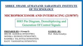
  • 1. SHREE SWAMI ATMANAND SARASWATI INSTITUTE OF TECHNOLOGY MICROPROCESSOR AND INTERFACING (2150707) PREPARED BY: ( Group:2) BHUMI AGHERA(130760107001) MONIKA DUDHAT(130760107007) RADHIKA TALAVIYA(130760107029) RAJVI VAGHASIYA(130760107031) 8085 Pin Diagram, Demultiplexing and Generation Of Control Signals GUIDED BY: Prof. Disha Goradiya
  • 2. INDEX 1. Introduction of 8085 microprocessor 2. Logic pinout of 8085 microprocessor 3. Demultiplexing 4. Generation of control signals
  • 3. The 8085 microprocessor • The term micro processing unit (MPU) is similar to the term central processing unit used in traditional computers. • The 8085 microprocessor can almost qualify as an MPU, but with the following two limitations. I. The low-order address bus of the 8085 microprocessor is multiplexed (time- shared) with the data bus. The buses need to be de-multiplexed. II. Appropriate control signals need to be generated to interface memory and I/O with the 8085. • The 8085 is an 8-bit general purpose microprocessor capable of addressing 64K of memory. • The device has forty pins, requires a +5 V single power supply, and can operate with a 3-MHz . Go To Index
  • 4. Logic pinout of the 8085 microprocessor Go To Index
  • 5. Logic pinout of the 8085 microprocessor • All the signals of 8085 pinout can be classified into Six groups: 1. Address bus 2. Data bus 3. Control and status signals 4. Power supply and frequency signals 5. Externally initiated signals 6. Serial I/O ports
  • 6. 1.Address Bus • The 8085 has 16 signal lines (pins) that are used as the address bus; however, these lines are split into two segments: A15 − A8 and AD7-AD0. • The eight signals lines, A15 − A8, are unidirectional and used as the most significant bits, called the high-order address, of a 16-bit address. • The signals lines, AD7-AD0 are used for a dual purpose.
  • 7. 2.Multiplexed Address/Data Bus • The signals lines AD7-AD0 are bidirectional they serve a dual purpose. • They are used as the low-order address bus as well as the data bus. • In executing an instruction, during the earlier part of the cycle, these lines are used as the low order address bus. During the later part of the cycle, these lines are used as the data bus. This is also known as multiplexing the bus. • However, the low order address bus can be separated from these signals by using a latch.
  • 8. 3.Contorl And Status Signals • This groups of signals include two control signals ( RD and WR ), three status signals ( IO/M, S1 and S2 ) to identify the nature of the operation, and one special signal(ALE) to indicate the beginning of the operation. These signals are as follows:  ALE- Address Latch Enable: This is a positive going pulse generated every time the 8085 begins an operation (machine cycle); it indicate that the bits on AD7-AD0 are address bus. This signal is used primarily to latch the low-order address from the multiplexed bus and generate a separate set of eight address lines, A7-A0.  RD-Read: This is a read control signal(active low). This signal indicates that the selected I/O or memory device is to be read and data are available on data bus.  WR-Write: This is a write control signal(active low). This signal indicate that the data on bus are to be written into selected memory/IO location.
  • 9. 3.Contorl And Status Signals  IO/ 𝑀: This is a status signal used to differentiate between I/O and memory operation. When it is high, it indicates an I/O operation, when it is low, it indicate a memory operation. This signal is combined with 𝑅𝐷(read) and 𝑊𝑅(write) to generate I/O or memory control signal.  𝑆1 and 𝑆2: These status signal, similar to IO/ 𝑀, can identify various operation. But they are rarely used in small system.
  • 10. 8085 Machine cycle and Control Signals Machine Cycle Status IO/ 𝑴 𝑆1 𝑆 𝟐 Control Signals Opcode Fetch 0 1 1 RD=0 Memory Read 0 1 0 RD=0 Memory Write 0 0 1 WR=0 I/O Read 1 1 0 RD=0 I/O Write 1 0 1 WR=0 Interrupt Acknowledge 1 1 1 INTA=0 Halt Z 0 0 Hold Z X X RD, WR=Z and INTA=1 Reset Z X X NOTE: Z: Tri state (High impedance) X: Unspecified
  • 11. 4.Power supply and clock frequency • VCC: +5 volt supply • VSS: Ground Reference • X1, X2: A crystal or RC,LC network is connected at this two pins. The frequency is internally divided into two; therefore, to operate a system at 3 MHz, the crystal should have a frequency of 6 MHz . • CLK (OUT)-Clock Output: this signal can be used as the system clock for other devices.
  • 12. 5.Externally initiated signals • INTR (Input) – Interrupt Request: this is used as a general-purpose interrupt; it is similar to the INT signal of the 8080A. • INTA (Output) – Interrupt Acknowledge: this is used to acknowledge an interrupt. • RST 7.5, RST 6.5, RST 5.5 (Inputs) – Restart interrupts: These are vectored interrupts that transfer the program control to specific memory locations. They have higher priorities than the INTR interrupt. Among these three, the priority order is 7.5, 6.5 and 5.5. • TRAP (Input) : This is a nonmaskable interrupt and has the highest priority. • HOLD (Input): This signal indicates that a peripheral such as a DMA controller is requesting the use of the address and data buses. • HLDA (Output) – Hold Acknowledge: This signal acknowledges the HOLD reques
  • 13. 5.Externally initiated signals • READY (Input): This signal is used to delay the microprocessor Read and Write cycles until a slow-responding peripheral is ready to send or accept data. When this signal goes low, the microprocessor waits for an integral number of clock cycles until it goes high. • RESET IN: When the signal on this pin goes low,the program counter is set to zero, the buses are tri-stated and the MPU is reset. • RESET OUT: This signal indicates that the MPU is being reset. The signal can be used to reset other devices.
  • 14. 6.Serial I/O ports • The 8085 has two signals to implement the serial transmission: SID(Serial Input Data) and SOD(Serial Output Data). • In serial transmission, data bits are sent over a single line, one bit at a time, such as the transmission over telephone lines. • SID (Input): Serial input data line. The data on this line is loaded into accumulator bit 7 whenever a RIM instruction is executed. • SOD (output): Serial output data line. The output SOD is set or reset as specified by the SIM instruction.
  • 15. Demultiplexing of bus 𝐴𝐷7-𝐴𝐷0 • Figure 1 shows a schematic that uses a latch and the ALE signal to demultiplex the bus. • The bus 𝐴7-𝐴0 is connected as the input to the latch 74LS373. The ALE signal is connected to Enable(G) pin of the latch, and the output control (𝑂𝐶) signal of the latch is grounded. • When ALE is high, the latch is transparent; this means that the output changes according to input data. • When ALE goes low, the data byte is latches until the next ALE, and the output of latch represents the low-order address bus 𝐴7-𝐴0 after latching operation. • Intel has circumvented the problem of demultiplexing the low-order bus by designing special devices such as the 8155(256 bytes of R/W memory + I/Os), which is compatible with the 8085 multiplexed bus. These devices internally demultiplex the bus using the ALE signal. Go To Index
  • 16. Demultiplexing of bus 𝐴𝐷7-𝐴𝐷0 Fig. 1 Schematic of Latching Low-Order Address Bus
  • 17. Definition • Instruction cycle : Instruction cycle is defined as the time required to complete the execution of an instruction. The 8085 instruction cycle consists of one to six machine cycle or one to six operations. • Machine cycle : Machine cycle is defined as the time required to complete one operation of accessing memory, I/O or acknowledging an external request. This cycle may consist of three to six T-states. • T-state : T-state is defined as one subdivision of the operation performed in one clock period. This subdivisions are internal states synchronized with the system clock, and each T- state is precisely equal to one clock period. The term T-state and clock period are often used synonymously. Go To Index
  • 18. Generating Control Signals • The RD (Read) is used both for reading memory and for reading an input device., it is necessary to generate two different Read signals: one memory and another for input. Similarly, two separate Write signals must be generated. • Figure (a) shows that four different control signals are generated by combining the signals 𝑅𝐷, 𝑊𝑅, and IO/ 𝑀. • The signal IO/ 𝑀 goes low for the memory operation. This signal is ANDed with 𝑅𝐷 and 𝑊𝑅 signals by using the 74LS32 quadruple two-input OR gates. • The OR gates are functionally connected as negative NAND gates. When both input signals go low, the outputs of the gates go low and generate 𝑀𝐸𝑀𝑅 (Memory Read) and 𝑀𝐸𝑀𝑊 (Memory Write)control signals. • When the IO/ 𝑀 signal goes high, it indicates the peripheral I/O operation. This signal is complemented using the Hex inverter 74LS04 and ANDed with the 𝑅𝐷 and 𝑊𝑅 signals to generate 𝐼𝑂𝑅 (I/O Read) and 𝐼𝑂𝑊 (I/O Write) control signals. Go To Index
  • 19.
  • 20. • To demultiplex the bus and to generate the necessary control signals, the 8085 microprocessor requires a latch and logic gates to build the MPU. This MPU can be interfaced with any memory or I/O. Figure (b) 8085 Demultiplexed Address and Data Bus with Control Signals