Downloaded 727 times

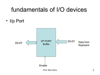
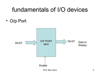

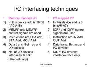
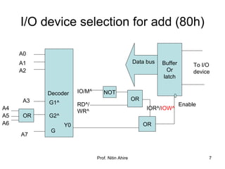
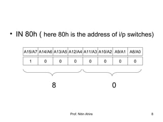
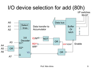
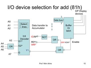

The document discusses input/output (I/O) interfacing techniques with the 8085 microprocessor. It describes the fundamentals of I/O devices like input and output ports, and how they are used to transfer data to and from devices like keyboards and displays. The document outlines two techniques for interfacing I/O devices: memory mapped I/O which uses memory addresses and instructions to transfer data, and I/O mapped I/O which uses dedicated I/O addresses and instructions. Circuits for decoding addresses to select specific I/O devices are also presented.


![8051 singed number concept [compatibility mode]](https://cdn.slidesharecdn.com/ss_thumbnails/8051singednumberconceptcompatibilitymode-130827015258-phpapp02-thumbnail.jpg?width=640&height=640&fit=bounds)


