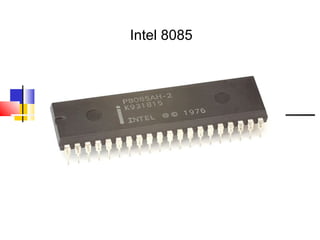
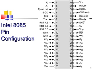
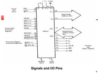
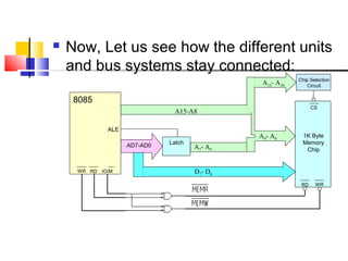
An Introduction to 
Microprocessor Architecture 
using intel 8085 as a classic 
processor 
http://educate.intel.com/en/TheJourneyInside/ExploreTheCurriculum/EC_Microprocessors/
Intel 8085
33 
IInntteell 88008855 
PPiinn 
CCoonnffiigguurraattiioonn
44 
Signals and I/O Pins
55 
IInntteell 88008855 CCPPUU BBlloocckk DDiiaaggrraamm
The 8085 and Its Buses 
 The 8085 is an 8-bit general purpose microprocessor that can 
address 64K Byte of memory. 
 It has 40 pins and uses +5V for power. It can run at a maximum 
frequency of 3 MHz. 
 The pins on the chip can be grouped into 6 groups: 
 Address Bus. 
 Data Bus. 
 Control and Status Signals. 
 Power supply and frequency. 
 Externally Initiated Signals. 
 Serial I/O ports.
The Address and Data Bus Systems 
 The address bus has 8 signal lines A8 – A15 which are 
unidirectional. 
 The other 8 address bits are multiplexed (time shared) with the 
8 data bits. 
 So, the bits AD0 – AD7 are bi-directional and serve as A0 – 
A7 and D0 – D7 at the same time. 
 During the execution of the instruction, these lines carry 
the address bits during the early part, then during the 
late parts of the execution, they carry the 8 data bits. 
 In order to separate the address from the data, we can use a 
latch to save the value before the function of the bits 
changes.
ALE used to demultiplex address/data bus 
8
The Control and Status 
Signals 
 There are 4 main control and status signals. These are: 
 ALE: Address Latch Enable. This signal is a pulse that 
become 1 when the AD0 – AD7 lines have an address 
on them. It becomes 0 after that. This signal can be used 
to enable a latch to save the address bits from the AD 
lines. 
 RD: Read. Active low. 
 WR: Write. Active low. 
 IO/M: This signal specifies whether the operation is a 
memory operation (IO/M=0) or an I/O operation 
(IO/M=1). 
 S1 and S0 : Status signals to specify the kind of 
operation being performed. Usually not used in small 
systems.
Frequency Control Signals 
 There are 3 important pins in the frequency control group. 
 X0 and X1 are the inputs from the crystal or clock generating 
circuit. 
 The frequency is internally divided by 2. 
 So, to run the microprocessor at 3 MHz, a clock 
running at 6 MHz should be connected to the X0 and 
X1 pins. 
 CLK (OUT): An output clock pin to drive the clock of the rest 
of the system. 
 We will discuss the rest of the control signals as we get to them.
A closer look at the 8085 
Architecture 
 Now, let’s look at some of its features 
with more details.
The ALU 
 In addition to the arithmetic & logic circuits, the ALU 
includes an accumulator, which is a part of every 
arithmetic & logic operation. 
 Also, the ALU includes a temporary register used for 
holding data temporarily during the execution of the 
operation. This temporary register is not accessible 
by the programmer.
The Flags register 
 There is also a flag register whose bits are affected by the arithmetic & 
logic operations. 
 S-sign flag 
 The sign flag is set if bit D7 of the accumulator is set after an 
arithmetic or logic operation. 
 Z-zero flag 
 Set if the result of the ALU operation is 0. Otherwise is reset. 
This flag is affected by operations on the accumulator as well 
as other registers. (DCR B). 
 AC-Auxiliary Carry 
 This flag is set when a carry is generated from bit D3 and 
passed to D4 . This flag is used only internally for BCD 
operations. 
 P-Parity flag 
 After an ALU operation, if the result has an even # of 1s, the 
p-flag is set. Otherwise it is cleared. So, the flag can be used 
to indicate even parity. 
 CY-carry flag 
 This flag is set when a carry is generated from bit D7 after an 
unsigned operation. 
 OV-Overflow flag 
 This flag is set when an overflow occurs after a signed 
operation.
 Now, Let us see how the different units 
and bus systems stay connected: 
A15-A8 
AD7-AD0 Latch 
A7- A0 
D7- D0 
8085 
ALE 
WR RD IO/M 
CS 
1K Byte 
Memory 
Chip 
RD WR 
A15- A10 
A9- A0 
Chip Selection 
Circuit
More on the 8085 machine 
cycles 
 The 8085 executes several types of instructions 
with each requiring a different number of 
operations of different types. However, the 
operations can be grouped into a small set. 
 The three main types are: 
 Memory Read and Write. 
 I/O Read and Write. 
 Request Acknowledge. 
 These can be further divided into various smaller 
operations (machine cycles).
Opcode Fetch Machine Cycle 
 The first step of executing any instruction is the Opcode fetch 
cycle. 
 In this cycle, the microprocessor brings in the instruction’s 
Opcode from memory. 
 To differentiate this machine cycle from the very similar 
“memory read” cycle, the control & status signals are set 
as follows: 
 IO/M=0, s0 and s1 are both 1. 
 This machine cycle has four T-states. 
 The 8085 uses the first 3 T-states to fetch the opcode. 
 T4 is used to decode and execute it. 
 It is also possible for an instruction to have 6 T-states in an 
opcode fetch machine cycle.
Memory Read Machine Cycle 
 The memory read machine cycle is 
exactly the same as the opcode fetch 
except: 
 It only has 3 T-states 
 The s0 signal is set to 0 instead.
The Memory Read Machine Cycle 
 To understand the memory read machine cycle, let’s 
study the execution of the following instruction: 
 MVI A, 32 
 In memory, this instruction looks like: 
2000H 
2001H 
3E 
32 
 The first byte 3EH represents the opcode for loading 
a byte into the accumulator (MVI A), the second byte 
is the data to be loaded. 
 The 8085 needs to read these two bytes from memory 
before it can execute the instruction. Therefore, it will 
need at least two machine cycles. 
 The first machine cycle is the opcode fetch 
discussed earlier. 
 The second machine cycle is the Memory Read 
Cycle.
Machine Cycles vs. Number of bytes 
in the instruction 
 Machine cycles and instruction length, do not have a direct 
relationship. 
 To illustrate, let’s look at the machine cycles needed to 
execute the following instruction. 
 STA 2065H 
 This is a 3-byte instruction requiring 4 machine 
cycles and 13 T-states. 
 The machine code will be stored 
in memory as shown to the right 
 This instruction requires the following 4 machine cycles: 
2010H 
2011H 
2012H 
32H 
65H 
20H 
 A ‘Opcode fetch’ to fetch the opcode (32H) from location 2010H, ‘decode’ it 
and determine that 2 more bytes are needed (4 T-states). 
 A ‘Memory read’ to read the low order byte of the address (65H) (3 T-states). 
 A ‘Memory read’ to read the high order byte of the address (20H) (3 T-states). 
 A ‘memory write’ to write the contents of the accumulator into the memory 
location.
The Memory Write Operation 
 In a memory write operation: 
 The 8085 places the address (2065H) on the 
address bus 
 Identifies the operation as a ‘memory write’ 
(IO/M=0, s1=0, s0=1). 
 Places the contents of the accumulator on the 
data bus and asserts the signal WR. 
 During the last T-state, the contents of the data 
bus are saved into the memory location.
Memory interfacing 
 There needs to be a lot of interaction between the 
microprocessor and the memory for the exchange of 
information during program execution. 
 Memory has its requirements on control signals 
and their timing. 
 The microprocessor has its requirements as well. 
 The interfacing operation is simply the matching of 
these requirements.
Memory structure & its requirements 
Address 
Lines 
ROM 
Output Buffer RD 
Date 
Lines 
CS 
RAM 
Address 
Lines 
Data Lines 
Input Buffer WR 
Output Buffer RD 
Data Lines 
CS 
 The way of interfacing the above two chips to the 
microprocessor is the same. 
 However, the ROM does not have a WR signal.
Interfacing Memory 
 Accessing memory can be summarized into the following three 
steps: 
 Select the chip. 
 Identify the memory register. 
 Enable the appropriate buffer. 
 Translating this to microprocessor domain: 
 The microprocessor places a 16-bit address on the 
address bus. 
 Part of the address bus will select the chip and the 
other part will go through the address decoder to 
select the register. 
 The signals IO/M and RD combined indicate that a 
memory read operation is in progress. The MEMR 
signal can be used to enable the RD line on the 
memory chip.
Address decoding 
 The result of ‘address decoding’ is the 
identification of a register for a given address. 
 A large part of the address bus is usually 
connected directly to the address inputs of the 
memory chip. 
 This portion is decoded internally within the 
chip. 
 What concerns us is the other part that must 
be decoded externally to select the chip. 
 This can be done either using logic gates or a 
decoder.
Putting all of the concepts together: 
Back to the Overall Picture  
A15-A8 
AD7-AD0 Latch 
A7- A0 
D7- D0 
8085 
ALE 
WR RD IO/M 
CS 
1K Byte 
Memory 
Chip 
RD WR 
A15- A10 
A9- A0 
Chip Selection 
Circuit
Control and Status Signals. 
26
27 
Interrupt Signals 
 8085 μp has several interrupt signals as shown in the 
following table.
28 
Interrupt signals 
 An interrupt is a hardware-initiated subroutine CALL. 
 When interrupt pin is activated, an ISR will be called, 
interrupting the program that is currently executing. 
PPiinn SSuubbrroouuttiinnee LLooccaattiioonn 
TTRRAAPP 00002244 
RRSSTT 55..55 000022CC 
RRSSTT 66..55 00003344 
RRSSTT 77..55 000033CC 
IINNTTRR ** 
NNoottee:: ** tthhee aaddddrreessss ooff tthhee IISSRR iiss ddeetteerrmmiinneedd bbyy tthhee eexxtteerrnnaall hhaarrddwwaarree..
29 
Interrupt signals 
 INTR input is enabled when EI instruction 
is executed. 
 The status of the RST 7.5, RST 6.5 and 
RST 5.5 pins are determined by both EI 
instruction and the condition of the mask 
bits in the interrupt mask register.
30 
Interrupt 
Vectors
A circuit that causes an RST4 instruction (E7) to be 
executed in response to INTR. 
31 
 When INTR is 
asserted, 
8085 
response with 
INTA pulse. 
 During INTA 
pulse, 8085 
expect to see 
an instruction 
applied to its 
data bus.
RESET signal 
 Following are the two kind of RESET 
signals: 
 RESET IN: an active low input signal, Program 
Counter (PC) will be set to 0 and thus MPU will 
reset. 
 RESET OUT: an output reset signal to indicate 
that the μp was reset (i.e. RESET IN=0). It 
also used to reset external devices. 
32
33 
RESET signal
34 
Direct Memory Access (DMA) 
 DMA is an IO technique where external IO device 
requests the use of the MPU buses. 
 Allows external IO devices to gain high speed access to 
the memory. 
 Example of IO devices that use DMA: disk memory system. 
 HOLD and HLDA are used for DMA. 
 If HOLD=1, 8085 will place it address, data and control 
pins at their high-impedance. 
 A DMA acknowledgement is signaled by HLDA=1.
MPU Communication and Bus Timing 
Figure 3: Moving data form memory to MPU using instruction MOV C, A 
(code machine 4FH = 0100 1111) 
35
MPU Communication and Bus Timing 
 The Fetch Execute Sequence : 
1. The μp placed a 16 bit memory address from 
PC (program counter) to address bus. 
36 
– Figure 4: at T1 
– The high order address, 20H, is placed at A15 – A8. 
– the low order address, 05H, is placed at AD7 - AD0 and 
ALE is active high. 
– Synchronously the IO/M is in active low condition to show it 
is a memory operation. 
1. At T2 the active low control signal, RD, is 
activated so as to activate read operation; it is to 
indicate that the MPU is in fetch mode 
operation.
MPU Communication and Bus Timing 
37 Figure 4: 8085 timing diagram for Opcode fetch cycle for MOV C, A .
MPU Communication and Bus Timing 
3. T3: The active low RD signal enabled 
the byte instruction, 4FH, to be placed 
on AD7 – AD0 and transferred to the 
MPU. While RD high, the data bus will 
be in high impedance mode. 
4. T4: The machine code, 4FH, will then 
be decoded in instruction decoder. The 
content of accumulator (A) will then 
copied into C register at time state, T4. 
38

8085 (1)

  • 1.
    An Introduction to Microprocessor Architecture using intel 8085 as a classic processor http://educate.intel.com/en/TheJourneyInside/ExploreTheCurriculum/EC_Microprocessors/
  • 2.
  • 3.
    33 IInntteell 88008855 PPiinn CCoonnffiigguurraattiioonn
  • 4.
  • 5.
    55 IInntteell 88008855CCPPUU BBlloocckk DDiiaaggrraamm
  • 6.
    The 8085 andIts Buses  The 8085 is an 8-bit general purpose microprocessor that can address 64K Byte of memory.  It has 40 pins and uses +5V for power. It can run at a maximum frequency of 3 MHz.  The pins on the chip can be grouped into 6 groups:  Address Bus.  Data Bus.  Control and Status Signals.  Power supply and frequency.  Externally Initiated Signals.  Serial I/O ports.
  • 7.
    The Address andData Bus Systems  The address bus has 8 signal lines A8 – A15 which are unidirectional.  The other 8 address bits are multiplexed (time shared) with the 8 data bits.  So, the bits AD0 – AD7 are bi-directional and serve as A0 – A7 and D0 – D7 at the same time.  During the execution of the instruction, these lines carry the address bits during the early part, then during the late parts of the execution, they carry the 8 data bits.  In order to separate the address from the data, we can use a latch to save the value before the function of the bits changes.
  • 8.
    ALE used todemultiplex address/data bus 8
  • 9.
    The Control andStatus Signals  There are 4 main control and status signals. These are:  ALE: Address Latch Enable. This signal is a pulse that become 1 when the AD0 – AD7 lines have an address on them. It becomes 0 after that. This signal can be used to enable a latch to save the address bits from the AD lines.  RD: Read. Active low.  WR: Write. Active low.  IO/M: This signal specifies whether the operation is a memory operation (IO/M=0) or an I/O operation (IO/M=1).  S1 and S0 : Status signals to specify the kind of operation being performed. Usually not used in small systems.
  • 10.
    Frequency Control Signals  There are 3 important pins in the frequency control group.  X0 and X1 are the inputs from the crystal or clock generating circuit.  The frequency is internally divided by 2.  So, to run the microprocessor at 3 MHz, a clock running at 6 MHz should be connected to the X0 and X1 pins.  CLK (OUT): An output clock pin to drive the clock of the rest of the system.  We will discuss the rest of the control signals as we get to them.
  • 11.
    A closer lookat the 8085 Architecture  Now, let’s look at some of its features with more details.
  • 12.
    The ALU In addition to the arithmetic & logic circuits, the ALU includes an accumulator, which is a part of every arithmetic & logic operation.  Also, the ALU includes a temporary register used for holding data temporarily during the execution of the operation. This temporary register is not accessible by the programmer.
  • 13.
    The Flags register  There is also a flag register whose bits are affected by the arithmetic & logic operations.  S-sign flag  The sign flag is set if bit D7 of the accumulator is set after an arithmetic or logic operation.  Z-zero flag  Set if the result of the ALU operation is 0. Otherwise is reset. This flag is affected by operations on the accumulator as well as other registers. (DCR B).  AC-Auxiliary Carry  This flag is set when a carry is generated from bit D3 and passed to D4 . This flag is used only internally for BCD operations.  P-Parity flag  After an ALU operation, if the result has an even # of 1s, the p-flag is set. Otherwise it is cleared. So, the flag can be used to indicate even parity.  CY-carry flag  This flag is set when a carry is generated from bit D7 after an unsigned operation.  OV-Overflow flag  This flag is set when an overflow occurs after a signed operation.
  • 14.
     Now, Letus see how the different units and bus systems stay connected: A15-A8 AD7-AD0 Latch A7- A0 D7- D0 8085 ALE WR RD IO/M CS 1K Byte Memory Chip RD WR A15- A10 A9- A0 Chip Selection Circuit
  • 15.
    More on the8085 machine cycles  The 8085 executes several types of instructions with each requiring a different number of operations of different types. However, the operations can be grouped into a small set.  The three main types are:  Memory Read and Write.  I/O Read and Write.  Request Acknowledge.  These can be further divided into various smaller operations (machine cycles).
  • 16.
    Opcode Fetch MachineCycle  The first step of executing any instruction is the Opcode fetch cycle.  In this cycle, the microprocessor brings in the instruction’s Opcode from memory.  To differentiate this machine cycle from the very similar “memory read” cycle, the control & status signals are set as follows:  IO/M=0, s0 and s1 are both 1.  This machine cycle has four T-states.  The 8085 uses the first 3 T-states to fetch the opcode.  T4 is used to decode and execute it.  It is also possible for an instruction to have 6 T-states in an opcode fetch machine cycle.
  • 17.
    Memory Read MachineCycle  The memory read machine cycle is exactly the same as the opcode fetch except:  It only has 3 T-states  The s0 signal is set to 0 instead.
  • 18.
    The Memory ReadMachine Cycle  To understand the memory read machine cycle, let’s study the execution of the following instruction:  MVI A, 32  In memory, this instruction looks like: 2000H 2001H 3E 32  The first byte 3EH represents the opcode for loading a byte into the accumulator (MVI A), the second byte is the data to be loaded.  The 8085 needs to read these two bytes from memory before it can execute the instruction. Therefore, it will need at least two machine cycles.  The first machine cycle is the opcode fetch discussed earlier.  The second machine cycle is the Memory Read Cycle.
  • 19.
    Machine Cycles vs.Number of bytes in the instruction  Machine cycles and instruction length, do not have a direct relationship.  To illustrate, let’s look at the machine cycles needed to execute the following instruction.  STA 2065H  This is a 3-byte instruction requiring 4 machine cycles and 13 T-states.  The machine code will be stored in memory as shown to the right  This instruction requires the following 4 machine cycles: 2010H 2011H 2012H 32H 65H 20H  A ‘Opcode fetch’ to fetch the opcode (32H) from location 2010H, ‘decode’ it and determine that 2 more bytes are needed (4 T-states).  A ‘Memory read’ to read the low order byte of the address (65H) (3 T-states).  A ‘Memory read’ to read the high order byte of the address (20H) (3 T-states).  A ‘memory write’ to write the contents of the accumulator into the memory location.
  • 20.
    The Memory WriteOperation  In a memory write operation:  The 8085 places the address (2065H) on the address bus  Identifies the operation as a ‘memory write’ (IO/M=0, s1=0, s0=1).  Places the contents of the accumulator on the data bus and asserts the signal WR.  During the last T-state, the contents of the data bus are saved into the memory location.
  • 21.
    Memory interfacing There needs to be a lot of interaction between the microprocessor and the memory for the exchange of information during program execution.  Memory has its requirements on control signals and their timing.  The microprocessor has its requirements as well.  The interfacing operation is simply the matching of these requirements.
  • 22.
    Memory structure &its requirements Address Lines ROM Output Buffer RD Date Lines CS RAM Address Lines Data Lines Input Buffer WR Output Buffer RD Data Lines CS  The way of interfacing the above two chips to the microprocessor is the same.  However, the ROM does not have a WR signal.
  • 23.
    Interfacing Memory Accessing memory can be summarized into the following three steps:  Select the chip.  Identify the memory register.  Enable the appropriate buffer.  Translating this to microprocessor domain:  The microprocessor places a 16-bit address on the address bus.  Part of the address bus will select the chip and the other part will go through the address decoder to select the register.  The signals IO/M and RD combined indicate that a memory read operation is in progress. The MEMR signal can be used to enable the RD line on the memory chip.
  • 24.
    Address decoding The result of ‘address decoding’ is the identification of a register for a given address.  A large part of the address bus is usually connected directly to the address inputs of the memory chip.  This portion is decoded internally within the chip.  What concerns us is the other part that must be decoded externally to select the chip.  This can be done either using logic gates or a decoder.
  • 25.
    Putting all ofthe concepts together: Back to the Overall Picture  A15-A8 AD7-AD0 Latch A7- A0 D7- D0 8085 ALE WR RD IO/M CS 1K Byte Memory Chip RD WR A15- A10 A9- A0 Chip Selection Circuit
  • 26.
    Control and StatusSignals. 26
  • 27.
    27 Interrupt Signals  8085 μp has several interrupt signals as shown in the following table.
  • 28.
    28 Interrupt signals  An interrupt is a hardware-initiated subroutine CALL.  When interrupt pin is activated, an ISR will be called, interrupting the program that is currently executing. PPiinn SSuubbrroouuttiinnee LLooccaattiioonn TTRRAAPP 00002244 RRSSTT 55..55 000022CC RRSSTT 66..55 00003344 RRSSTT 77..55 000033CC IINNTTRR ** NNoottee:: ** tthhee aaddddrreessss ooff tthhee IISSRR iiss ddeetteerrmmiinneedd bbyy tthhee eexxtteerrnnaall hhaarrddwwaarree..
  • 29.
    29 Interrupt signals  INTR input is enabled when EI instruction is executed.  The status of the RST 7.5, RST 6.5 and RST 5.5 pins are determined by both EI instruction and the condition of the mask bits in the interrupt mask register.
  • 30.
  • 31.
    A circuit thatcauses an RST4 instruction (E7) to be executed in response to INTR. 31  When INTR is asserted, 8085 response with INTA pulse.  During INTA pulse, 8085 expect to see an instruction applied to its data bus.
  • 32.
    RESET signal Following are the two kind of RESET signals:  RESET IN: an active low input signal, Program Counter (PC) will be set to 0 and thus MPU will reset.  RESET OUT: an output reset signal to indicate that the μp was reset (i.e. RESET IN=0). It also used to reset external devices. 32
  • 33.
  • 34.
    34 Direct MemoryAccess (DMA)  DMA is an IO technique where external IO device requests the use of the MPU buses.  Allows external IO devices to gain high speed access to the memory.  Example of IO devices that use DMA: disk memory system.  HOLD and HLDA are used for DMA.  If HOLD=1, 8085 will place it address, data and control pins at their high-impedance.  A DMA acknowledgement is signaled by HLDA=1.
  • 35.
    MPU Communication andBus Timing Figure 3: Moving data form memory to MPU using instruction MOV C, A (code machine 4FH = 0100 1111) 35
  • 36.
    MPU Communication andBus Timing  The Fetch Execute Sequence : 1. The μp placed a 16 bit memory address from PC (program counter) to address bus. 36 – Figure 4: at T1 – The high order address, 20H, is placed at A15 – A8. – the low order address, 05H, is placed at AD7 - AD0 and ALE is active high. – Synchronously the IO/M is in active low condition to show it is a memory operation. 1. At T2 the active low control signal, RD, is activated so as to activate read operation; it is to indicate that the MPU is in fetch mode operation.
  • 37.
    MPU Communication andBus Timing 37 Figure 4: 8085 timing diagram for Opcode fetch cycle for MOV C, A .
  • 38.
    MPU Communication andBus Timing 3. T3: The active low RD signal enabled the byte instruction, 4FH, to be placed on AD7 – AD0 and transferred to the MPU. While RD high, the data bus will be in high impedance mode. 4. T4: The machine code, 4FH, will then be decoded in instruction decoder. The content of accumulator (A) will then copied into C register at time state, T4. 38