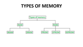
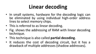
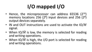
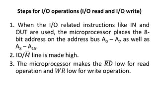
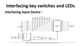
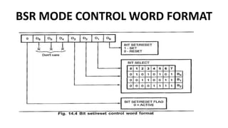
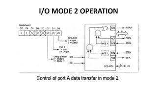
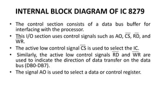
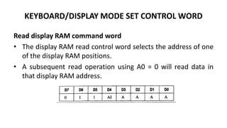
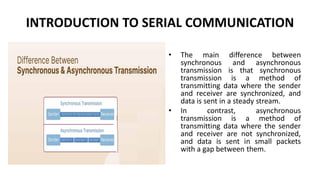
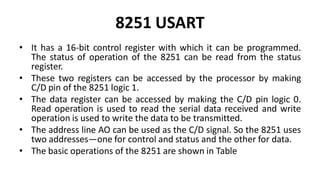
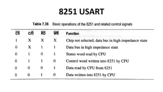
IT T44 - MICROPROCESSORS AND
MICROCONTROLLERS
Dr.A.Shankar
Associate Professor
Department of ECE
UNIT III
MEMORY & I/O INTERFACING
SYLLABUS
Memory & I/O Interfacing: Types of memory –
Memory mapping and addressing – Concept of
I/O map – types – I/O decode logic – Interfacing
key switches and LEDs – 8279 Keyboard/Display
Interface - 8255 Programmable Peripheral
Interface – Concept of Serial Communication –
8251 USART – RS232C Interface.
TYPES OF MEMORY
MEMORY INTERFACING
• Memory interfacing is used to provide more memory
space to accommodate complex programs for more
complicated systems.
• Types of memories which are most commonly used to
interface with 8085 are RAM, ROM, and EEPROM.
• 8085 can access 64kB of external memory.
• It can be explained as- total number of address lines in
8085 are 16, therefore it can access 2^16 = 65535
locations i.e. 64kB.
MEMORY INTERFACING
• Partial decoding
• In this type of decoding not all the address
lines are utilized in the circuit (they are left as
unused pins).
• Ex: In an interface of 4kB memory only A0-A11
address lines are utilized, whereas the
remaining A12-A15 address lines are unused.
MEMORY INTERFACING
• Complete decoding (exhaustive decoding):
• In this type of decoding, all the address lines are
utilized in circuit for some or the other use (i.e. all
pins are exhausted).
• Ex: In an interface of 4kB memory only A0-A11
address lines are utilized, whereas the remaining
A12-A15 address lines are used in Memory
selection logic or as any other control signals.
MEMORY MAPPING AND ADDRESSING
Memory Interfacing in 8085
• Memory is an integral part of a microprocessor system,
and in this section, we will discuss how to interface a
memory device with the microprocessor.
• The Memory Interfacing in 8085 is used to access
memory quite frequently to read instruction codes and
data stored in memory.
• This read/write operations are monitored by control
signals.
Address Decoding Techniques
• Absolute decoding/Full Decoding
• Linear decoding/Partial Decoding
Absolute decoding
• In absolute decoding technique, all the higher address
lines are decoded to select the memory chip, and the
memory chip is selected only for the specified logic
levels on these high-order address lines; no other logic
levels can select the chip.
• Fig. shows the Memory Interfacing in 8085 with
absolute decoding.
• This addressing technique is normally used in large
memory systems.
Absolute decoding
Linear decoding
• In small systems, hardware for the decoding logic can
be eliminated by using individual high-order address
lines to select memory chips.
• This is referred to as linear decoding.
• Fig. shows the addressing of RAM with linear decoding
technique.
• This technique is also called partial decoding.
• It reduces the cost of decoding circuit, but it has a
drawback of multiple addresses (shadow addresses).
Linear decoding
I/O mapped I/O
I/O mapped I/O
• In this method, I/O devices are treated as I/O devices and memory
is treated as memory.
• Separate address space is used for memory and I/O. The I/O
mapped I/O scheme is shown in figure
• In I/O mapped I/O scheme, the microprocessor uses the sixteen
address lines A0 – A7 and A8 – A15 for the memory and eight address
lines A0 to A7 to identify an input / output device.
• Here, the full address space 0000 – FFFF is used for the memory
and a separate address space 00 – FF is used for the I/O devices.
I/O mapped I/O
• Hence, the microprocessor can address 65536 (216)
memory locations 256 (28) input devices and 256 (28)
output devices separately.
• IN and OUT instructions are used to activate the IO/𝑀
signal.
• When IO/𝑀 is low, the memory is selected for reading
and writing operations.
• When IO/𝑀 is high, the I/O port is selected for reading
and writing operations.
Steps for I/O operations (I/O read and I/O write)
1. When the I/O related instructions like IN and
OUT are used, the microprocessor places the 8-
bit address on the address bus A0 – A7 as well as
A8 – A15.
2. IO/𝑀 line is made high.
3. The microprocessor makes the 𝑅𝐷 low for read
operation and 𝑊𝑅 low for write operation.
Interfacing key switches and LEDs
Interfacing Input Device :
Interfacing key switches and LEDs
• The microprocessor 8085 accepts 8 bit data from the input device
such as keyboard, sensors, transducers etc.
• Fig. shows the circuit diagram to Input Output Interfacing
Techniques (buffer) which is used to read the status of 8 switches.
• The address for this input device is 80H as device select signal goes
low when address is 80H.
• When the switch is in the released position, the status of line is high
otherwise status is low. With this information microprocessor can
check a particular key is pressed or not.
• The following program checks whether the switch 2 is pressed or
not
Interfacing key switches and LEDs
• Interfacing Output Device :
Interfacing key switches and LEDs
• The microprocessor 8085 sends 8 bit data to the output
device such as 7 segment displays, LEDs, printer etc.
• Fig shows the circuit diagram to interface output port
(latch) which is used to send the signal for glowing the
LEDs. LED will glow when output pin status is low.
• The IC 74LS138 and 3 input OR gate is used to generate
device select signal.
• The latch enable signal is active high. So NOR gate is used
to generate latch enable signal, which goes high when Y1
and IOW both are low.
INTEL 8255 PROGRAMMABLE PERIPHERAL INTERFACE
• The Intel 8085 microprocessor can transfer data between
external devices such as input and output devices through
ports.
• Normally, a register can act as an I/O port.
• However, using a separate register and configuring it for
input and output operations is both difficult and tedious.
• So Intel has designed a separate IC, the 8255, with the
objective of interfacing input and output devices with Intel
microprocessors.
• The 8255 is used with a wide range of I/O cards that plug
into an available slot in a PC.
INTEL 8255 PROGRAMMABLE PERIPHERAL INTERFACE
• The 8255 programmable peripheral interface (PPI) is a
very popular and versatile I/O chip that can be easily
programmed to function in several different
configurations.
• This chip can perform digital input and output (DIO)
from the processor in a preprogrammed manner.
• The common applications of the 8255 with the 8085
include sensing a switch, controlling movement by use
of motors, and detecting a position.
FEATURES OF 8255
(i) It has three 8-bit ports A, B, and C connected to the output pins.
(ii) Port C is divided into two groups, port C upper (PCU) and port C
lower (PCL), of 4 bits each. Each of them can be programmed
independently or as 4-bit ports, for input and output operations.
(iii) All the ports can be programmed for simple I/O or handshake I/O
in the input/output mode.
(iv) Each port C bit can be set/reset individually in bit set/reset mode.
(v) The bits of port A and PCU are grouped as group A (GA).
(vi) The bits of port B and PCL are grouped as group B (GB).
BLOCK DIAGRAM OF INTEL 8255
• The block diagram of the 8255 shows ports A,
B, and C and groups A and B. In addition, there
is another register called control register.
• The contents written into the control register
decide the operating modes of the three
parallel ports.
BLOCK DIAGRAM OF INTEL 8255
• To identify the four registers, the 8255 uses two address lines—A0 and A1.
• These lines get their signals from the 8085 processor address bus.
• The identification of the registers based on A0 and A1 is given in Table
BLOCK DIAGRAM OF INTEL 8255
• The pin details of the 8255 are given in Fig. The three ports of the
8255 need eight lines each.
• So 24 pins are allotted for the ports and these lines are connected
to external input or output devices. D0-D7 are the lines required for
interfacing the 8255 with the processor.
• These data lines are connected to the data bus of the processor.
• Eight lines or pins are remaining.
• Out of these eight lines, two lines—A0 and A1—are allotted for
selecting one of the four registers available in the 8255. The control
signals for reading from and writing into these registers are the
active low RD and WR signals.
BLOCK DIAGRAM OF INTEL 8255
• These signals are obtained from the processor’s control
signals.
• The chip is selected by activating the active low chip
select (CS) signal.
• This signal is obtained from the decoder, which
decodes the 8085 address lines and identifies the 8255
address range.
• A common reset signal such as the RESET OUT of the
8085 processor can be applied to reset the 8255.
PIN DETAILS OF IC 8255
OPERATING MODES AND CONTROL WORDS OF 8255
• The function of each port in the 8255 is
software-programmed by the programmer.
• This is done by writing a control word in its
control register.
• The control word contains information such as
mode, bit set, bit reset, etc., which initialize
the functional configuration of the 8255.
OPERATING MODES AND CONTROL WORDS OF 8255
• Figure shows the basic operating modes of the 8255.
• There are two configurations in the 8255—I/O mode and
bit set/reset mode (BSR mode).
• In I/O mode, there are three modes for the ports. The
programmer can select a particular operating mode using
commands and control words.
• The three ports of the 8255 are grouped as groups A and B.
Groups A and B accept commands from the read/ write
control logic, receive control words from the internal data
bus, and issue commands to the associated ports.
I/O MODE CONTROL WORD FORMAT
• The MSB D7 is set to 1 to indicate that the chip is configured in I/O
mode.
• Bits D6 and D5 are used to select the operating mode of group A.
• There are three basic modes of operation for group A:
(i) Mode 0—Basic I/O (bits D6 and D5 are both 0)—Ports A and B and
the higher-order four bits of port C can be operated as inputs or
outputs. This mode uses simple I/O operation; no interrupts are
used. The outputs written into the ports are latched and available
at any time. Inputs available at the port pins are buffered through
port latches.
I/O MODE CONTROL WORD FORMAT
(ii) Mode 1—Strobed or handshake input/output (bits D6 and
D5 are 0 and 1, respectively)—Port A is configured in mode
1, while port C is used for handshaking and control of data
transfer in Port A. Input and output data are latched.
(iii) Mode 2—Bidirectional I/O mode (bits D6 and D5 are 1 and
X, respectively)— Port A is bidirectional (i.e., both input and
output), while port C is used for handshaking. Port B cannot
be programmed to this mode.
I/O MODE CONTROL WORD FORMAT
• Bit D4 is used to select the direction of data flow in the port
A bits, i.e., it decides whether the port A pins are input pins
(D4 = 1) or output pins (D4 = 0).
• Bit D3 is used to decide whether the four higher-order bits
of port C are used for input (D3 = 1) or output (D3 = 0).
• Bit D2 of the control word is used to select the mode for
group B.
• As discussed earlier, only two operating modes—mode 0
and mode 1—are possible for group B.
BSR MODE CONTROL WORD FORMAT
• In BSR mode, any of the eight bits of port C can be set
or reset using a single control word written into the
control register.
• This feature helps the programmer to control the port
C pin outputs individually.
• It is also used in mode 1 and mode 2 I/O operations,
wherein the individual ports of port C can be controlled
by the programmer to indicate the status and control.
I/O MODE 1 OPERATION
CONTROL AND HANDSHAKE SIGNAL FOR INPUT OPERATION IN MODE 1
I/O MODE 1 OPERATION
CONTROL AND HANDSHAKE SIGNAL FOR INPUT OPERATION IN MODE 1
I/O MODE 1 OPERATION
CONTROL AND HANDSHAKE SIGNALS FOR OUTPUT OPERATION IN MODE 1
I/O MODE 1 OPERATION
CONTROL AND HANDSHAKE SIGNALS FOR OUTPUT OPERATION IN MODE 1
I/O MODE 2 OPERATION
FEATURES OF 8279
IC 8279 is a programmable keyboard and display interface controller, designed by Intel
for use with Intel microprocessors.
The major features of this IC are as follows:
(i) Supports keyboard of size up to 64-key matrix with 2-key lockout and n- key rollover
options
(ii) Supports display interface of up to 16 digits with many options
(iii) Simultaneous keyboard and display operations
(iv) 8-character FIFO memory to store the codes of keys pressed
(v) 16-byte display RAM corresponding to 16 digits of display
INTERNAL BLOCK DIAGRAM OF IC 8279
IC 8279 has the following three sections:
(i)Display section with its own display RAM
(ii)Keyboard scan section with FIFO registers
(iii)Control logic with signals for interfacing with the
processor
INTERNAL BLOCK DIAGRAM OF IC 8279
• The control section consists of a data bus buffer for
interfacing with the processor.
• This I/O section uses control signals such as AO, CS, RD, and
WR.
• The active low control signal CS is used to select the IC.
• Similarly, the active low control signals RD and WR are
used to indicate the direction of data transfer on the data
bus (DB0-DB7).
• The signal AO is used to select a data or control register.
2-key lockout & N-key rollover
• In the 2-key lockout mode, if two keys are
pressed simultaneously, only the first key is
recognized.
• In the N-key rollover mode, simultaneous keys
are recognized and their codes are stored in
FIFO. The keyboard section also has an 8 x 8
FIFO (First In First Out) RAM.
INTERNAL BLOCK DIAGRAM OF IC 8279
• A logic 1 on the A0 line means that the content of
the data bus is a command or status.
• A logic 0 on the line means that the content of
the data bus is data for the IC.
• The control and timing registers store the
keyboard and display modes and other operating
conditions.
INTERNAL BLOCK DIAGRAM OF IC 8279
• Although there are many control and data registers, the
8279 uses only two addresses—one with A0 = 0 and the
other with A0 = 1.
• This is done using a unique control word for each
operation.
• For example, two different control words are available for
accessing the display RAM and the keyboard FIFO.
• For every operation, the corresponding control word is
written, the necessary register is accessed, and then the
operation is carried out.
INTERNAL BLOCK DIAGRAM OF IC 8279
• SL0-SL3 are the four scan lines of the 8279.
• There are two programmable options for the scan lines—encoded
mode and decoded mode.
• In encoded mode, the SL0-SL3 lines are binary counter outputs and
need to be decoded externally for scanning keyboards and displays.
• In decoded mode, the SL3-SL0 outputs are decoded; one of the four
lines has an active low output.
• The scan lines SL0-SL3 are common to both keyboards and displays.
RL0-RL7 are the eight return lines and are used as inputs to sense a
key press in the keyboard matrix.
PIN DIAGRAM OF IC 8279
• The other signals available in the 8279 are as follows:
(i) BD: Active low output signal, used to blank all displays
(ii)CLK: Clock input to be given to the 8279, for proper
operation of internal circuits
(iii)CNTL/STB: Control or strobe signal, given as input from
the control key in the keyboard
(iv)Shift: Input to the 8279 from the shift key of the
keyboard
PIN DIAGRAM OF IC 8279
(v)IRQ: Interrupt request sent to the processor
from the 8279 to indicate a key press
(vi)OUT A0-A3 and OUT B0-B3: Data output lines
for the display units
(vii)Reset: Input to the 8279 and connected to
the processor RESET OUT
KEYBOARD/DISPLAY MODE SET CONTROL WORD
Clock Signal Programming Command Word
• The clock command word programs the internal clock driver. The code PPPPP
shown in Fig. corresponds to the binary code by which the input clock signal must
be divided to achieve the desired operating frequency.
• With the five bits D0-D4, division is possible by any number from two to 31.
• For example, for an operating frequency of 100 kHz and a clock input of 1 MHz,
the count should be 0101 OB (i.e., 10D). This control word decides the time taken
for scanning and the de-bouncing.
KEYBOARD/DISPLAY MODE SET CONTROL WORD
Read FIFO Sensor RAM Command Word
• The read FIFO control word selects the address (AAA) of a keystroke from the FIFO buffer
(000-111).
• The bit AI shown in Fig. selects auto-increment for the address. If AI is set to 1, the address
will be incremented after every read operation.
• So data is fetched continuously, one after another, from the FIFO to the processor.
• In the scan keyboard mode, the AAA and AI bits become irrelevant. All data from the FIFO are
read consecutively in the same order in which they were entered into the FIFO.
KEYBOARD/DISPLAY MODE SET CONTROL WORD
Write Display RAM Command Word
• Writing the above command into the command register programs the 8279 to get
and store the data to be displayed in the display RAM.
• If AI is set to 1, the auto increment option is implemented and the address of the
RAM is incremented automatically after every write operation.
• Data written with 0 in the address line AO are written into subsequent RAM
addresses, automatically incrementing them. The write display RAM control word
format is shown in Fig
KEYBOARD/DISPLAY MODE SET CONTROL WORD
Read display RAM command word
• The display RAM read control word selects the address of one
of the display RAM positions.
• A subsequent read operation using A0 = 0 will read data in
that display RAM address.
KEYBOARD/DISPLAY MODE SET CONTROL WORD
Clear display command word
• The clear display control word can clear the display RAM using the CD bits.
• This command word has the option of making the display RAM all Os (D3
and D2 = 0) or all Is (D3 and D2 = 1).
• Setting CF bit is used to clear the keyboard FIFO RAM. Setting CA bit is
used to clear both the display RAM and the FIFO RAM.
KEY DEBOUNCE
• The push buttons used for interfacing switches
to microprocessors based systems when
pressed bounces for certain number of times ,
before reaching a steady state.
• Hence microprocessor waits until it reaches
the steady state. This is known as key
debouncing.
INTRODUCTION TO SERIAL COMMUNICATION
• Serial communication is the process of sending and receiving information
bit by bit.
• For short-range communication, parallel data transfer is preferable as it is
the fastest means.
• When used over long distances, parallel communication needs numerous
wires and complex error handling/data recovery mechanisms.
• Moreover, for parallel data transmission of n bits, both the receiver- and
the transmitter- side equipments need n separate amplifiers and related
hardware. This results in complex circuitry and high cost.
• Thus, serial communication is preferred for long- range communication. It
can be easily implemented using a single wire or a pair of wires.
INTRODUCTION TO SERIAL COMMUNICATION
• Serial data can be sent either in synchronous mode or asynchronous
mode.
• In synchronous transmission, data is sent in blocks at a constant rate, i.e.,
the frequencies of transmission and reception are the same.
• Transmission and reception take place simultaneously. The beginning and
end of a block are identified with specific bytes or bit patterns.
• In general, synchronous transmission is used for high transmission speeds
of more than 20 k bits/second. In asynchronous transmission, each data
character has a bit to identify its start and one or two bits to identify its
end. Here, each character is identified individually.
• The characters can be sent at any time, without checking the receiver.
Reception and transmission are not synchronized.
INTRODUCTION TO SERIAL COMMUNICATION
• The main difference between
synchronous and asynchronous
transmission is that synchronous
transmission is a method of
transmitting data where the sender
and receiver are synchronized, and
data is sent in a steady stream.
• In contrast, asynchronous
transmission is a method of
transmitting data where the sender
and receiver are not synchronized,
and data is sent in small packets
with a gap between them.
8251 USART
• The 8251 is a universal synchronous asynchronous receiver
transmitter (USART) used for serial data communication.
• As a peripheral device in a microcomputer system, the 8251
receives parallel data from the CPU and transmits them in serial
form.
• This device also receives serial data from outside, converts them
into parallel data, and sends them to the CPU.
• The 8251 can support both synchronous and asynchronous
transmission formats and is programmable.
• It supports full-duplex serial transmission and reception and
variable baud rates.
Simplex , Duplex and Full Duplex
8251 USART
8251 USART
• It consists of a parallel-to-serial shift register for transmission over
the TXD line from the buffer and a serial-to-parallel converter for
data received on the RXD line.
• A separate control unit is available to determine the operation of the
IC according to the control word written into it.
• A modem control unit is present for interfacing a modem with the
8251.
• In addition to these units, IC 8251 has an I/O port that can be used
for interfacing with any processor along with its read and write
control logic.
• The 8251 requires clock and reset signals for working in a
synchronized manner with the processor
8251 USART
• It has a 16-bit control register with which it can be programmed.
The status of operation of the 8251 can be read from the status
register.
• These two registers can be accessed by the processor by making
C/D pin of the 8251 logic 1.
• The data register can be accessed by making the C/D pin logic 0.
Read operation is used to read the serial data received and write
operation is used to write the data to be transmitted.
• The address line AO can be used as the C/D signal. So the 8251 uses
two addresses—one for control and status and the other for data.
• The basic operations of the 8251 are shown in Table
8251 USART
8251 USART
The 8251 has 28 pins. The details and functions of these pins are listed here.
(i) Data bus (D0-D7): A group of bidirectional lines that are used for data and
control word transfer between the CPU and the 8251
(ii) Reset: An active high signal applied to reset IC 8251. After resetting, the IC
has to be initialized again starting from the mode word.
(iii) CLK: The input signal used to apply a clock frequency to IC 8251. This
signal is used for the internal timing of all operations. This CLK frequency
must be higher than the transmit and receive clock frequency.
(iv) WR: Active low input signal, used to write data or command into IC 8251
(v) RD: Active low input signal, used to read data or status from IC 8251
(vi) C/D: Input signal used to select command/status or data. Input of 0
indicates command/status; input of 1 indicates data.
8251 USART
(vii) CS: Active low input signal, used to select IC 8251. Any operation with the
IC can be done only when the CS signal is active low.
(viii) TXD: Transmit data line, used to send data out from the 8251
(ix) TXRDY (Transmit ready): Active high signal sent by the 8251 to the
processor, indicating that it is ready to accept a byte of data for transfer.
(x) TXEMPTY (Transmit buffer empty): Active high output signal, used to
indicate that the output register for transmitting data is empty.
8251 USART
(xi) TXC (Transmitter clock): Input clock signal used for transmitting or
shifting data to TXD line. The frequency of this signal decides the
transmit baud rate.
(xii) RXD: Receive data line, used to receive data from another USART
(xiii)RXRDY (Receiver ready): Active high output signal to the processor,
indicating that it is ready with the received data.
(xiv) RXC (Receiver clock): Input clock signal, used for receiving and shifting
data on the RXD to the buffer. The frequency of this signal decides the
receive baud rate.
(xv) SYNDET/BD: Active high output. In asynchronous mode, it is used to
indicate a data break. In synchronous mode, it is used to indicate the
correct receipt of synchronous characters and the next data to be
received.
8251 USART
The following signals are used with a modem for handshaking and
establishing connection:
(i) DTR: Active low output signal sent out by the 8251 to the modem,
to indicate that it is ready for communication
(ii) DSR: Active low input signal sent by the modem to indicate that it is
ready to transmit or receive
(iii) RTS: Active low output signal to the modem by the 8251, indicating
that it is ready to send data
(iv) CTS: Active low input signal sent by the modem, indicating that it
can accept data for transmission
MODE COMMAND WORD
SERIAL COMMAND WORD
RS-232 INTERFACE
• In telecommunications, RS-232 or Recommended Standard 232 is a
standard originally introduced in 1960 for serial communication
transmission of data.
• RS-232 is an interface for the interchange of serial binary data between
two devices.
• It is a standard protocol used for serial communication; it is used for
connecting a computer and its peripheral devices to allow serial data
exchange between them.
• The standard was introduced in the 1960s by the Electronic Industries
Association (EIA), a trade organization that later became known as the
Electronic Industries Alliance, until it ceased operations in February 2011.
RS-232 INTERFACE
RS-232 INTERFACE
• Communication defined by RS-232 is serial data
communication
• There is a single wire or link for each direction of data
flow and the bits of the message are sent in sequence
one at a time
• Compared to parallel systems where multiple lines
carry many data bites simultaneously, serial
communication requires less circuitry at either end of
the data link.
RS-232 INTERFACE
• All though RS-232 standard defines a serial system
with just a single wire for each direction , the standard
allows for other signal wires the DTE and DCE as well
• These additional signals are used to manage the data
interface and to indicate communication status at any
time to both the DTE device and the DCE device
• The RS-232 specification is intended to provide reliable
communication up to a distances of soft, at rate up to
20000 baud rate .
RS-232 INTERFACE
• In RS232, ‘RS’ stands for Recommended Standard. It
defines the serial communication using DTE and DCE
signals.
• Here, DTE refers to Data Terminal Equipment and DCE
refers to the Data Communication Equipment.
• Example of DTE device is a computer and DCE is a
modem. Formally, it is specified as the interface
between DTE equipment and DCE equipment using
serial binary data exchange.
RS-232 INTERFACE
RS-232 INTERFACE
• The DTE (computer) transmits the information serially to
the other end equipment DCE (modem).
• In this case, DTE sends binary data “11011101” to DCE and
DCE sends binary data “11010101” to the DTE device.
• RS232 describes the common voltage levels, electrical
standards, operation mode and number of bits to be
transferred from DTE to DCE.
• This standard is used for transmission of information
exchange over the telephone lines.
Communication Interface
Functional Description
RS-232 INTERFACE
• Advantages
• Simple protocol design.
• Hardware overhead is lesser than parallel
communication.
• Recommended standard for short distance
applications.
• Compatible with DTE and DCE communication.
• Low cost protocol for development.
RS-232 INTERFACE
• Disadvantages
• The limitations of RS232 protocol are, it doesn’t
support full-duplex communication and it is a single-
ended protocol which shifts the ground potential.
• Moreover, the longer cable length introduces cross
talk during serial communication.
• Hence, this protocol is restricted for long distance
communication.
RS-232 INTERFACE
• Applications
• RS232 communication is used in different applications. Some of them are:
• Teletypewriter devices.
• Demodulator applications.
• PC COM port interfacing.
• In embedded systems for debugging.
• Modems and printers.
• Handheld equipment.
• CNC controllers, Software debuggers etc.
• Barcode scanners and Point of Sales (POS) terminals.

Micro Processor And Micro Controller for engineering in Pondicherry University

  • 1.
    IT T44 -MICROPROCESSORS AND MICROCONTROLLERS Dr.A.Shankar Associate Professor Department of ECE
  • 2.
    UNIT III MEMORY &I/O INTERFACING
  • 3.
    SYLLABUS Memory & I/OInterfacing: Types of memory – Memory mapping and addressing – Concept of I/O map – types – I/O decode logic – Interfacing key switches and LEDs – 8279 Keyboard/Display Interface - 8255 Programmable Peripheral Interface – Concept of Serial Communication – 8251 USART – RS232C Interface.
  • 4.
  • 5.
    MEMORY INTERFACING • Memoryinterfacing is used to provide more memory space to accommodate complex programs for more complicated systems. • Types of memories which are most commonly used to interface with 8085 are RAM, ROM, and EEPROM. • 8085 can access 64kB of external memory. • It can be explained as- total number of address lines in 8085 are 16, therefore it can access 2^16 = 65535 locations i.e. 64kB.
  • 6.
    MEMORY INTERFACING • Partialdecoding • In this type of decoding not all the address lines are utilized in the circuit (they are left as unused pins). • Ex: In an interface of 4kB memory only A0-A11 address lines are utilized, whereas the remaining A12-A15 address lines are unused.
  • 7.
    MEMORY INTERFACING • Completedecoding (exhaustive decoding): • In this type of decoding, all the address lines are utilized in circuit for some or the other use (i.e. all pins are exhausted). • Ex: In an interface of 4kB memory only A0-A11 address lines are utilized, whereas the remaining A12-A15 address lines are used in Memory selection logic or as any other control signals.
  • 8.
  • 9.
    Memory Interfacing in8085 • Memory is an integral part of a microprocessor system, and in this section, we will discuss how to interface a memory device with the microprocessor. • The Memory Interfacing in 8085 is used to access memory quite frequently to read instruction codes and data stored in memory. • This read/write operations are monitored by control signals.
  • 10.
    Address Decoding Techniques •Absolute decoding/Full Decoding • Linear decoding/Partial Decoding
  • 11.
    Absolute decoding • Inabsolute decoding technique, all the higher address lines are decoded to select the memory chip, and the memory chip is selected only for the specified logic levels on these high-order address lines; no other logic levels can select the chip. • Fig. shows the Memory Interfacing in 8085 with absolute decoding. • This addressing technique is normally used in large memory systems.
  • 12.
  • 13.
    Linear decoding • Insmall systems, hardware for the decoding logic can be eliminated by using individual high-order address lines to select memory chips. • This is referred to as linear decoding. • Fig. shows the addressing of RAM with linear decoding technique. • This technique is also called partial decoding. • It reduces the cost of decoding circuit, but it has a drawback of multiple addresses (shadow addresses).
  • 14.
  • 15.
  • 16.
    I/O mapped I/O •In this method, I/O devices are treated as I/O devices and memory is treated as memory. • Separate address space is used for memory and I/O. The I/O mapped I/O scheme is shown in figure • In I/O mapped I/O scheme, the microprocessor uses the sixteen address lines A0 – A7 and A8 – A15 for the memory and eight address lines A0 to A7 to identify an input / output device. • Here, the full address space 0000 – FFFF is used for the memory and a separate address space 00 – FF is used for the I/O devices.
  • 17.
    I/O mapped I/O •Hence, the microprocessor can address 65536 (216) memory locations 256 (28) input devices and 256 (28) output devices separately. • IN and OUT instructions are used to activate the IO/𝑀 signal. • When IO/𝑀 is low, the memory is selected for reading and writing operations. • When IO/𝑀 is high, the I/O port is selected for reading and writing operations.
  • 18.
    Steps for I/Ooperations (I/O read and I/O write) 1. When the I/O related instructions like IN and OUT are used, the microprocessor places the 8- bit address on the address bus A0 – A7 as well as A8 – A15. 2. IO/𝑀 line is made high. 3. The microprocessor makes the 𝑅𝐷 low for read operation and 𝑊𝑅 low for write operation.
  • 19.
    Interfacing key switchesand LEDs Interfacing Input Device :
  • 20.
    Interfacing key switchesand LEDs • The microprocessor 8085 accepts 8 bit data from the input device such as keyboard, sensors, transducers etc. • Fig. shows the circuit diagram to Input Output Interfacing Techniques (buffer) which is used to read the status of 8 switches. • The address for this input device is 80H as device select signal goes low when address is 80H. • When the switch is in the released position, the status of line is high otherwise status is low. With this information microprocessor can check a particular key is pressed or not. • The following program checks whether the switch 2 is pressed or not
  • 21.
    Interfacing key switchesand LEDs • Interfacing Output Device :
  • 22.
    Interfacing key switchesand LEDs • The microprocessor 8085 sends 8 bit data to the output device such as 7 segment displays, LEDs, printer etc. • Fig shows the circuit diagram to interface output port (latch) which is used to send the signal for glowing the LEDs. LED will glow when output pin status is low. • The IC 74LS138 and 3 input OR gate is used to generate device select signal. • The latch enable signal is active high. So NOR gate is used to generate latch enable signal, which goes high when Y1 and IOW both are low.
  • 23.
    INTEL 8255 PROGRAMMABLEPERIPHERAL INTERFACE • The Intel 8085 microprocessor can transfer data between external devices such as input and output devices through ports. • Normally, a register can act as an I/O port. • However, using a separate register and configuring it for input and output operations is both difficult and tedious. • So Intel has designed a separate IC, the 8255, with the objective of interfacing input and output devices with Intel microprocessors. • The 8255 is used with a wide range of I/O cards that plug into an available slot in a PC.
  • 24.
    INTEL 8255 PROGRAMMABLEPERIPHERAL INTERFACE • The 8255 programmable peripheral interface (PPI) is a very popular and versatile I/O chip that can be easily programmed to function in several different configurations. • This chip can perform digital input and output (DIO) from the processor in a preprogrammed manner. • The common applications of the 8255 with the 8085 include sensing a switch, controlling movement by use of motors, and detecting a position.
  • 25.
    FEATURES OF 8255 (i)It has three 8-bit ports A, B, and C connected to the output pins. (ii) Port C is divided into two groups, port C upper (PCU) and port C lower (PCL), of 4 bits each. Each of them can be programmed independently or as 4-bit ports, for input and output operations. (iii) All the ports can be programmed for simple I/O or handshake I/O in the input/output mode. (iv) Each port C bit can be set/reset individually in bit set/reset mode. (v) The bits of port A and PCU are grouped as group A (GA). (vi) The bits of port B and PCL are grouped as group B (GB).
  • 26.
    BLOCK DIAGRAM OFINTEL 8255
  • 27.
    BLOCK DIAGRAM OFINTEL 8255 • The block diagram of the 8255 shows ports A, B, and C and groups A and B. In addition, there is another register called control register. • The contents written into the control register decide the operating modes of the three parallel ports.
  • 28.
    BLOCK DIAGRAM OFINTEL 8255 • To identify the four registers, the 8255 uses two address lines—A0 and A1. • These lines get their signals from the 8085 processor address bus. • The identification of the registers based on A0 and A1 is given in Table
  • 29.
    BLOCK DIAGRAM OFINTEL 8255 • The pin details of the 8255 are given in Fig. The three ports of the 8255 need eight lines each. • So 24 pins are allotted for the ports and these lines are connected to external input or output devices. D0-D7 are the lines required for interfacing the 8255 with the processor. • These data lines are connected to the data bus of the processor. • Eight lines or pins are remaining. • Out of these eight lines, two lines—A0 and A1—are allotted for selecting one of the four registers available in the 8255. The control signals for reading from and writing into these registers are the active low RD and WR signals.
  • 30.
    BLOCK DIAGRAM OFINTEL 8255 • These signals are obtained from the processor’s control signals. • The chip is selected by activating the active low chip select (CS) signal. • This signal is obtained from the decoder, which decodes the 8085 address lines and identifies the 8255 address range. • A common reset signal such as the RESET OUT of the 8085 processor can be applied to reset the 8255.
  • 31.
  • 32.
    OPERATING MODES ANDCONTROL WORDS OF 8255 • The function of each port in the 8255 is software-programmed by the programmer. • This is done by writing a control word in its control register. • The control word contains information such as mode, bit set, bit reset, etc., which initialize the functional configuration of the 8255.
  • 33.
    OPERATING MODES ANDCONTROL WORDS OF 8255
  • 34.
    OPERATING MODES ANDCONTROL WORDS OF 8255 • Figure shows the basic operating modes of the 8255. • There are two configurations in the 8255—I/O mode and bit set/reset mode (BSR mode). • In I/O mode, there are three modes for the ports. The programmer can select a particular operating mode using commands and control words. • The three ports of the 8255 are grouped as groups A and B. Groups A and B accept commands from the read/ write control logic, receive control words from the internal data bus, and issue commands to the associated ports.
  • 35.
    I/O MODE CONTROLWORD FORMAT
  • 36.
    I/O MODE CONTROLWORD FORMAT
  • 37.
    I/O MODE CONTROLWORD FORMAT • The MSB D7 is set to 1 to indicate that the chip is configured in I/O mode. • Bits D6 and D5 are used to select the operating mode of group A. • There are three basic modes of operation for group A: (i) Mode 0—Basic I/O (bits D6 and D5 are both 0)—Ports A and B and the higher-order four bits of port C can be operated as inputs or outputs. This mode uses simple I/O operation; no interrupts are used. The outputs written into the ports are latched and available at any time. Inputs available at the port pins are buffered through port latches.
  • 38.
    I/O MODE CONTROLWORD FORMAT (ii) Mode 1—Strobed or handshake input/output (bits D6 and D5 are 0 and 1, respectively)—Port A is configured in mode 1, while port C is used for handshaking and control of data transfer in Port A. Input and output data are latched. (iii) Mode 2—Bidirectional I/O mode (bits D6 and D5 are 1 and X, respectively)— Port A is bidirectional (i.e., both input and output), while port C is used for handshaking. Port B cannot be programmed to this mode.
  • 39.
    I/O MODE CONTROLWORD FORMAT • Bit D4 is used to select the direction of data flow in the port A bits, i.e., it decides whether the port A pins are input pins (D4 = 1) or output pins (D4 = 0). • Bit D3 is used to decide whether the four higher-order bits of port C are used for input (D3 = 1) or output (D3 = 0). • Bit D2 of the control word is used to select the mode for group B. • As discussed earlier, only two operating modes—mode 0 and mode 1—are possible for group B.
  • 40.
    BSR MODE CONTROLWORD FORMAT
  • 41.
    BSR MODE CONTROLWORD FORMAT
  • 42.
    BSR MODE CONTROLWORD FORMAT • In BSR mode, any of the eight bits of port C can be set or reset using a single control word written into the control register. • This feature helps the programmer to control the port C pin outputs individually. • It is also used in mode 1 and mode 2 I/O operations, wherein the individual ports of port C can be controlled by the programmer to indicate the status and control.
  • 43.
    I/O MODE 1OPERATION CONTROL AND HANDSHAKE SIGNAL FOR INPUT OPERATION IN MODE 1
  • 44.
    I/O MODE 1OPERATION CONTROL AND HANDSHAKE SIGNAL FOR INPUT OPERATION IN MODE 1
  • 45.
    I/O MODE 1OPERATION CONTROL AND HANDSHAKE SIGNALS FOR OUTPUT OPERATION IN MODE 1
  • 46.
    I/O MODE 1OPERATION CONTROL AND HANDSHAKE SIGNALS FOR OUTPUT OPERATION IN MODE 1
  • 47.
    I/O MODE 2OPERATION
  • 48.
    FEATURES OF 8279 IC8279 is a programmable keyboard and display interface controller, designed by Intel for use with Intel microprocessors. The major features of this IC are as follows: (i) Supports keyboard of size up to 64-key matrix with 2-key lockout and n- key rollover options (ii) Supports display interface of up to 16 digits with many options (iii) Simultaneous keyboard and display operations (iv) 8-character FIFO memory to store the codes of keys pressed (v) 16-byte display RAM corresponding to 16 digits of display
  • 49.
    INTERNAL BLOCK DIAGRAMOF IC 8279 IC 8279 has the following three sections: (i)Display section with its own display RAM (ii)Keyboard scan section with FIFO registers (iii)Control logic with signals for interfacing with the processor
  • 50.
    INTERNAL BLOCK DIAGRAMOF IC 8279 • The control section consists of a data bus buffer for interfacing with the processor. • This I/O section uses control signals such as AO, CS, RD, and WR. • The active low control signal CS is used to select the IC. • Similarly, the active low control signals RD and WR are used to indicate the direction of data transfer on the data bus (DB0-DB7). • The signal AO is used to select a data or control register.
  • 51.
    2-key lockout &N-key rollover • In the 2-key lockout mode, if two keys are pressed simultaneously, only the first key is recognized. • In the N-key rollover mode, simultaneous keys are recognized and their codes are stored in FIFO. The keyboard section also has an 8 x 8 FIFO (First In First Out) RAM.
  • 52.
  • 53.
    INTERNAL BLOCK DIAGRAMOF IC 8279 • A logic 1 on the A0 line means that the content of the data bus is a command or status. • A logic 0 on the line means that the content of the data bus is data for the IC. • The control and timing registers store the keyboard and display modes and other operating conditions.
  • 54.
    INTERNAL BLOCK DIAGRAMOF IC 8279 • Although there are many control and data registers, the 8279 uses only two addresses—one with A0 = 0 and the other with A0 = 1. • This is done using a unique control word for each operation. • For example, two different control words are available for accessing the display RAM and the keyboard FIFO. • For every operation, the corresponding control word is written, the necessary register is accessed, and then the operation is carried out.
  • 55.
    INTERNAL BLOCK DIAGRAMOF IC 8279 • SL0-SL3 are the four scan lines of the 8279. • There are two programmable options for the scan lines—encoded mode and decoded mode. • In encoded mode, the SL0-SL3 lines are binary counter outputs and need to be decoded externally for scanning keyboards and displays. • In decoded mode, the SL3-SL0 outputs are decoded; one of the four lines has an active low output. • The scan lines SL0-SL3 are common to both keyboards and displays. RL0-RL7 are the eight return lines and are used as inputs to sense a key press in the keyboard matrix.
  • 56.
  • 57.
    PIN DIAGRAM OFIC 8279 • The other signals available in the 8279 are as follows: (i) BD: Active low output signal, used to blank all displays (ii)CLK: Clock input to be given to the 8279, for proper operation of internal circuits (iii)CNTL/STB: Control or strobe signal, given as input from the control key in the keyboard (iv)Shift: Input to the 8279 from the shift key of the keyboard
  • 58.
    PIN DIAGRAM OFIC 8279 (v)IRQ: Interrupt request sent to the processor from the 8279 to indicate a key press (vi)OUT A0-A3 and OUT B0-B3: Data output lines for the display units (vii)Reset: Input to the 8279 and connected to the processor RESET OUT
  • 59.
  • 60.
  • 61.
    KEYBOARD/DISPLAY MODE SETCONTROL WORD Clock Signal Programming Command Word • The clock command word programs the internal clock driver. The code PPPPP shown in Fig. corresponds to the binary code by which the input clock signal must be divided to achieve the desired operating frequency. • With the five bits D0-D4, division is possible by any number from two to 31. • For example, for an operating frequency of 100 kHz and a clock input of 1 MHz, the count should be 0101 OB (i.e., 10D). This control word decides the time taken for scanning and the de-bouncing.
  • 62.
    KEYBOARD/DISPLAY MODE SETCONTROL WORD Read FIFO Sensor RAM Command Word • The read FIFO control word selects the address (AAA) of a keystroke from the FIFO buffer (000-111). • The bit AI shown in Fig. selects auto-increment for the address. If AI is set to 1, the address will be incremented after every read operation. • So data is fetched continuously, one after another, from the FIFO to the processor. • In the scan keyboard mode, the AAA and AI bits become irrelevant. All data from the FIFO are read consecutively in the same order in which they were entered into the FIFO.
  • 63.
    KEYBOARD/DISPLAY MODE SETCONTROL WORD Write Display RAM Command Word • Writing the above command into the command register programs the 8279 to get and store the data to be displayed in the display RAM. • If AI is set to 1, the auto increment option is implemented and the address of the RAM is incremented automatically after every write operation. • Data written with 0 in the address line AO are written into subsequent RAM addresses, automatically incrementing them. The write display RAM control word format is shown in Fig
  • 64.
    KEYBOARD/DISPLAY MODE SETCONTROL WORD Read display RAM command word • The display RAM read control word selects the address of one of the display RAM positions. • A subsequent read operation using A0 = 0 will read data in that display RAM address.
  • 65.
    KEYBOARD/DISPLAY MODE SETCONTROL WORD Clear display command word • The clear display control word can clear the display RAM using the CD bits. • This command word has the option of making the display RAM all Os (D3 and D2 = 0) or all Is (D3 and D2 = 1). • Setting CF bit is used to clear the keyboard FIFO RAM. Setting CA bit is used to clear both the display RAM and the FIFO RAM.
  • 66.
    KEY DEBOUNCE • Thepush buttons used for interfacing switches to microprocessors based systems when pressed bounces for certain number of times , before reaching a steady state. • Hence microprocessor waits until it reaches the steady state. This is known as key debouncing.
  • 67.
    INTRODUCTION TO SERIALCOMMUNICATION • Serial communication is the process of sending and receiving information bit by bit. • For short-range communication, parallel data transfer is preferable as it is the fastest means. • When used over long distances, parallel communication needs numerous wires and complex error handling/data recovery mechanisms. • Moreover, for parallel data transmission of n bits, both the receiver- and the transmitter- side equipments need n separate amplifiers and related hardware. This results in complex circuitry and high cost. • Thus, serial communication is preferred for long- range communication. It can be easily implemented using a single wire or a pair of wires.
  • 68.
    INTRODUCTION TO SERIALCOMMUNICATION • Serial data can be sent either in synchronous mode or asynchronous mode. • In synchronous transmission, data is sent in blocks at a constant rate, i.e., the frequencies of transmission and reception are the same. • Transmission and reception take place simultaneously. The beginning and end of a block are identified with specific bytes or bit patterns. • In general, synchronous transmission is used for high transmission speeds of more than 20 k bits/second. In asynchronous transmission, each data character has a bit to identify its start and one or two bits to identify its end. Here, each character is identified individually. • The characters can be sent at any time, without checking the receiver. Reception and transmission are not synchronized.
  • 69.
    INTRODUCTION TO SERIALCOMMUNICATION • The main difference between synchronous and asynchronous transmission is that synchronous transmission is a method of transmitting data where the sender and receiver are synchronized, and data is sent in a steady stream. • In contrast, asynchronous transmission is a method of transmitting data where the sender and receiver are not synchronized, and data is sent in small packets with a gap between them.
  • 70.
    8251 USART • The8251 is a universal synchronous asynchronous receiver transmitter (USART) used for serial data communication. • As a peripheral device in a microcomputer system, the 8251 receives parallel data from the CPU and transmits them in serial form. • This device also receives serial data from outside, converts them into parallel data, and sends them to the CPU. • The 8251 can support both synchronous and asynchronous transmission formats and is programmable. • It supports full-duplex serial transmission and reception and variable baud rates.
  • 71.
    Simplex , Duplexand Full Duplex
  • 72.
  • 73.
    8251 USART • Itconsists of a parallel-to-serial shift register for transmission over the TXD line from the buffer and a serial-to-parallel converter for data received on the RXD line. • A separate control unit is available to determine the operation of the IC according to the control word written into it. • A modem control unit is present for interfacing a modem with the 8251. • In addition to these units, IC 8251 has an I/O port that can be used for interfacing with any processor along with its read and write control logic. • The 8251 requires clock and reset signals for working in a synchronized manner with the processor
  • 74.
    8251 USART • Ithas a 16-bit control register with which it can be programmed. The status of operation of the 8251 can be read from the status register. • These two registers can be accessed by the processor by making C/D pin of the 8251 logic 1. • The data register can be accessed by making the C/D pin logic 0. Read operation is used to read the serial data received and write operation is used to write the data to be transmitted. • The address line AO can be used as the C/D signal. So the 8251 uses two addresses—one for control and status and the other for data. • The basic operations of the 8251 are shown in Table
  • 75.
  • 76.
    8251 USART The 8251has 28 pins. The details and functions of these pins are listed here. (i) Data bus (D0-D7): A group of bidirectional lines that are used for data and control word transfer between the CPU and the 8251 (ii) Reset: An active high signal applied to reset IC 8251. After resetting, the IC has to be initialized again starting from the mode word. (iii) CLK: The input signal used to apply a clock frequency to IC 8251. This signal is used for the internal timing of all operations. This CLK frequency must be higher than the transmit and receive clock frequency. (iv) WR: Active low input signal, used to write data or command into IC 8251 (v) RD: Active low input signal, used to read data or status from IC 8251 (vi) C/D: Input signal used to select command/status or data. Input of 0 indicates command/status; input of 1 indicates data.
  • 77.
    8251 USART (vii) CS:Active low input signal, used to select IC 8251. Any operation with the IC can be done only when the CS signal is active low. (viii) TXD: Transmit data line, used to send data out from the 8251 (ix) TXRDY (Transmit ready): Active high signal sent by the 8251 to the processor, indicating that it is ready to accept a byte of data for transfer. (x) TXEMPTY (Transmit buffer empty): Active high output signal, used to indicate that the output register for transmitting data is empty.
  • 78.
    8251 USART (xi) TXC(Transmitter clock): Input clock signal used for transmitting or shifting data to TXD line. The frequency of this signal decides the transmit baud rate. (xii) RXD: Receive data line, used to receive data from another USART (xiii)RXRDY (Receiver ready): Active high output signal to the processor, indicating that it is ready with the received data. (xiv) RXC (Receiver clock): Input clock signal, used for receiving and shifting data on the RXD to the buffer. The frequency of this signal decides the receive baud rate. (xv) SYNDET/BD: Active high output. In asynchronous mode, it is used to indicate a data break. In synchronous mode, it is used to indicate the correct receipt of synchronous characters and the next data to be received.
  • 79.
    8251 USART The followingsignals are used with a modem for handshaking and establishing connection: (i) DTR: Active low output signal sent out by the 8251 to the modem, to indicate that it is ready for communication (ii) DSR: Active low input signal sent by the modem to indicate that it is ready to transmit or receive (iii) RTS: Active low output signal to the modem by the 8251, indicating that it is ready to send data (iv) CTS: Active low input signal sent by the modem, indicating that it can accept data for transmission
  • 80.
  • 81.
  • 82.
    RS-232 INTERFACE • Intelecommunications, RS-232 or Recommended Standard 232 is a standard originally introduced in 1960 for serial communication transmission of data. • RS-232 is an interface for the interchange of serial binary data between two devices. • It is a standard protocol used for serial communication; it is used for connecting a computer and its peripheral devices to allow serial data exchange between them. • The standard was introduced in the 1960s by the Electronic Industries Association (EIA), a trade organization that later became known as the Electronic Industries Alliance, until it ceased operations in February 2011.
  • 83.
  • 84.
    RS-232 INTERFACE • Communicationdefined by RS-232 is serial data communication • There is a single wire or link for each direction of data flow and the bits of the message are sent in sequence one at a time • Compared to parallel systems where multiple lines carry many data bites simultaneously, serial communication requires less circuitry at either end of the data link.
  • 85.
    RS-232 INTERFACE • Allthough RS-232 standard defines a serial system with just a single wire for each direction , the standard allows for other signal wires the DTE and DCE as well • These additional signals are used to manage the data interface and to indicate communication status at any time to both the DTE device and the DCE device • The RS-232 specification is intended to provide reliable communication up to a distances of soft, at rate up to 20000 baud rate .
  • 86.
    RS-232 INTERFACE • InRS232, ‘RS’ stands for Recommended Standard. It defines the serial communication using DTE and DCE signals. • Here, DTE refers to Data Terminal Equipment and DCE refers to the Data Communication Equipment. • Example of DTE device is a computer and DCE is a modem. Formally, it is specified as the interface between DTE equipment and DCE equipment using serial binary data exchange.
  • 87.
  • 88.
    RS-232 INTERFACE • TheDTE (computer) transmits the information serially to the other end equipment DCE (modem). • In this case, DTE sends binary data “11011101” to DCE and DCE sends binary data “11010101” to the DTE device. • RS232 describes the common voltage levels, electrical standards, operation mode and number of bits to be transferred from DTE to DCE. • This standard is used for transmission of information exchange over the telephone lines.
  • 89.
  • 90.
  • 91.
    RS-232 INTERFACE • Advantages •Simple protocol design. • Hardware overhead is lesser than parallel communication. • Recommended standard for short distance applications. • Compatible with DTE and DCE communication. • Low cost protocol for development.
  • 92.
    RS-232 INTERFACE • Disadvantages •The limitations of RS232 protocol are, it doesn’t support full-duplex communication and it is a single- ended protocol which shifts the ground potential. • Moreover, the longer cable length introduces cross talk during serial communication. • Hence, this protocol is restricted for long distance communication.
  • 93.
    RS-232 INTERFACE • Applications •RS232 communication is used in different applications. Some of them are: • Teletypewriter devices. • Demodulator applications. • PC COM port interfacing. • In embedded systems for debugging. • Modems and printers. • Handheld equipment. • CNC controllers, Software debuggers etc. • Barcode scanners and Point of Sales (POS) terminals.