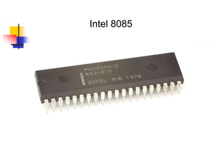
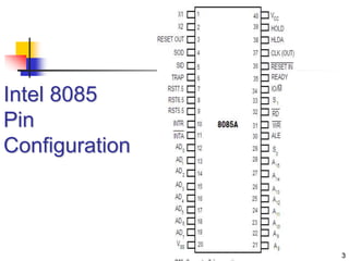
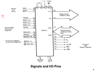
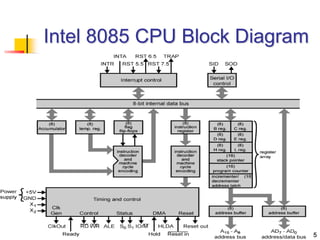
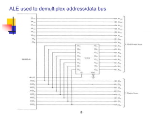
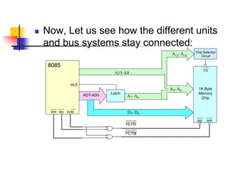
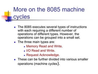
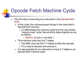
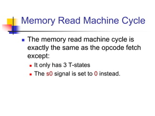
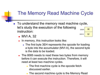
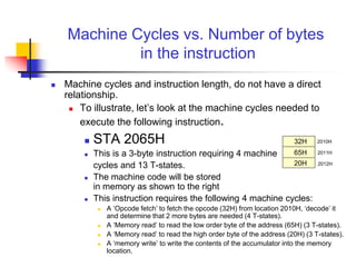
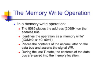
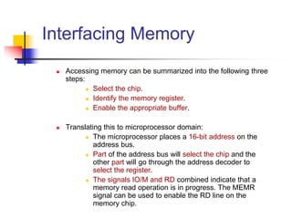
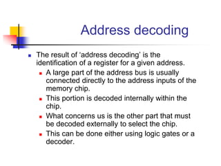
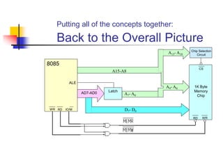
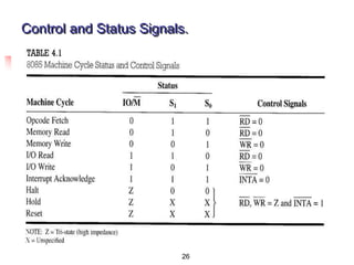
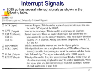
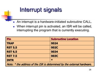
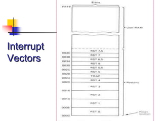
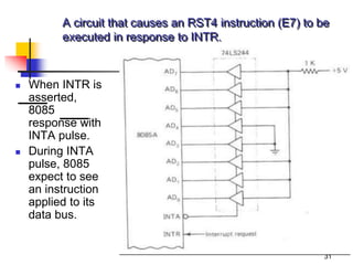
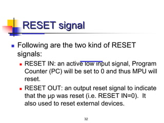
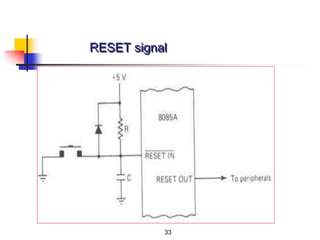
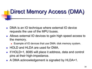
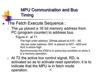
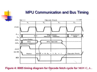
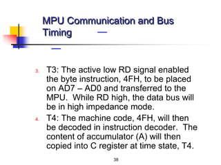
SlideShare a Scribd company logo
1 of 38
An Introduction to intel 8085
Microprocessor
www.mangroveinstitute.com
Intel 8085
3
Intel 8085
Pin
Configuration
4
Signals and I/O Pins
5
Intel 8085 CPU Block Diagram
The 8085 and Its Buses
īŽ The 8085 is an 8-bit general purpose microprocessor that can
address 64K Byte of memory.
īŽ It has 40 pins and uses +5V for power. It can run at a maximum
frequency of 3 MHz.
īŽ The pins on the chip can be grouped into 6 groups:
īŽ Address Bus.
īŽ Data Bus.
īŽ Control and Status Signals.
īŽ Power supply and frequency.
īŽ Externally Initiated Signals.
īŽ Serial I/O ports.
The Address and Data Bus Systems
īŽ The address bus has 8 signal lines A8 – A15 which are
unidirectional.
īŽ The other 8 address bits are multiplexed (time shared) with the
8 data bits.
īŽ So, the bits AD0 – AD7 are bi-directional and serve as A0 –
A7 and D0 – D7 at the same time.
īŽ During the execution of the instruction, these lines carry
the address bits during the early part, then during the late
parts of the execution, they carry the 8 data bits.
īŽ In order to separate the address from the data, we can use a
latch to save the value before the function of the bits
changes.
8
ALE used to demultiplex address/data bus
The Control and Status
Signals
īŽ There are 4 main control and status signals. These are:
īŽ ALE: Address Latch Enable. This signal is a pulse that
become 1 when the AD0 – AD7 lines have an address
on them. It becomes 0 after that. This signal can be used
to enable a latch to save the address bits from the AD
lines.
īŽ RD: Read. Active low.
īŽ WR: Write. Active low.
īŽ IO/M: This signal specifies whether the operation is a
memory operation (IO/M=0) or an I/O operation
(IO/M=1).
īŽ S1 and S0 : Status signals to specify the kind of
operation being performed. Usually not used in small
systems.
Frequency Control Signals
īŽ There are 3 important pins in the frequency control group.
īŽ X0 and X1 are the inputs from the crystal or clock generating
circuit.
īŽ The frequency is internally divided by 2.
īŽ So, to run the microprocessor at 3 MHz, a clock
running at 6 MHz should be connected to the X0 and
X1 pins.
īŽ CLK (OUT): An output clock pin to drive the clock of the rest
of the system.
īŽ We will discuss the rest of the control signals as we get to them.
A closer look at the 8085
Architecture
īŽ Now, let’s look at some of its features
with more details.
The ALU
īŽ In addition to the arithmetic & logic circuits, the ALU
includes an accumulator, which is a part of every
arithmetic & logic operation.
īŽ Also, the ALU includes a temporary register used for
holding data temporarily during the execution of the
operation. This temporary register is not accessible
by the programmer.
The Flags register
īŽ There is also a flag register whose bits are affected by the arithmetic &
logic operations.
īŽ S-sign flag
īŽ The sign flag is set if bit D7 of the accumulator is set after an
arithmetic or logic operation.
īŽ Z-zero flag
īŽ Set if the result of the ALU operation is 0. Otherwise is reset.
This flag is affected by operations on the accumulator as well
as other registers. (DCR B).
īŽ AC-Auxiliary Carry
īŽ This flag is set when a carry is generated from bit D3 and
passed to D4 . This flag is used only internally for BCD
operations.
īŽ P-Parity flag
īŽ After an ALU operation, if the result has an even # of 1s, the
p-flag is set. Otherwise it is cleared. So, the flag can be used
to indicate even parity.
īŽ CY-carry flag
īŽ This flag is set when a carry is generated from bit D7 after an
unsigned operation.
īŽ OV-Overflow flag
īŽ This flag is set when an overflow occurs after a signed
operation.
īŽ Now, Let us see how the different units
and bus systems stay connected:
A15-A8
Latch
AD7-AD0
D7- D0
A7- A0
8085
ALE
IO/M
RD
WR
1K Byte
Memory
Chip
WR
RD
CS
A9- A0
A15- A10
Chip Selection
Circuit
More on the 8085 machine
cycles
īŽ The 8085 executes several types of instructions
with each requiring a different number of
operations of different types. However, the
operations can be grouped into a small set.
īŽ The three main types are:
īŽ Memory Read and Write.
īŽ I/O Read and Write.
īŽ Request Acknowledge.
īŽ These can be further divided into various smaller
operations (machine cycles).
Opcode Fetch Machine Cycle
īŽ The first step of executing any instruction is the Opcode fetch
cycle.
īŽ In this cycle, the microprocessor brings in the instruction’s
Opcode from memory.
īŽ To differentiate this machine cycle from the very similar
“memory read” cycle, the control & status signals are set
as follows:
īŽ IO/M=0, s0 and s1 are both 1.
īŽ This machine cycle has four T-states.
īŽ The 8085 uses the first 3 T-states to fetch the opcode.
īŽ T4 is used to decode and execute it.
īŽ It is also possible for an instruction to have 6 T-states in an
opcode fetch machine cycle.
Memory Read Machine Cycle
īŽ The memory read machine cycle is
exactly the same as the opcode fetch
except:
īŽ It only has 3 T-states
īŽ The s0 signal is set to 0 instead.
The Memory Read Machine Cycle
īŽ To understand the memory read machine cycle,
let’s study the execution of the following
instruction:
īŽ MVI A, 32
īŽ In memory, this instruction looks like:
īŽ The first byte 3EH represents the opcode for loading
a byte into the accumulator (MVI A), the second byte
is the data to be loaded.
īŽ The 8085 needs to read these two bytes from memory
before it can execute the instruction. Therefore, it will
need at least two machine cycles.
īŽ The first machine cycle is the opcode fetch
discussed earlier.
īŽ The second machine cycle is the Memory Read
2000H
2001H
3E
32
Machine Cycles vs. Number of bytes
in the instruction
īŽ Machine cycles and instruction length, do not have a direct
relationship.
īŽ To illustrate, let’s look at the machine cycles needed to
execute the following instruction.
īŽ STA 2065H
īŽ This is a 3-byte instruction requiring 4 machine
cycles and 13 T-states.
īŽ The machine code will be stored
in memory as shown to the right
īŽ This instruction requires the following 4 machine cycles:
īŽ A ‘Opcode fetch’ to fetch the opcode (32H) from location 2010H, ‘decode’ it
and determine that 2 more bytes are needed (4 T-states).
īŽ A ‘Memory read’ to read the low order byte of the address (65H) (3 T-states).
īŽ A ‘Memory read’ to read the high order byte of the address (20H) (3 T-states).
īŽ A ‘memory write’ to write the contents of the accumulator into the memory
location.
2010H
2011H
2012H
32H
65H
20H
The Memory Write Operation
īŽ In a memory write operation:
īŽ The 8085 places the address (2065H) on the
address bus
īŽ Identifies the operation as a ‘memory write’
(IO/M=0, s1=0, s0=1).
īŽ Places the contents of the accumulator on the
data bus and asserts the signal WR.
īŽ During the last T-state, the contents of the data
bus are saved into the memory location.
Memory interfacing
īŽ There needs to be a lot of interaction between the
microprocessor and the memory for the exchange of
information during program execution.
īŽ Memory has its requirements on control signals
and their timing.
īŽ The microprocessor has its requirements as well.
īŽ The interfacing operation is simply the matching of
these requirements.
Memory structure & its requirements
īŽ The way of interfacing the above two chips to the
microprocessor is the same.
īŽ However, the ROM does not have a WR signal.
Address
Lines
Date
Lines
CS
RD
Output Buffer
ROM
Address
Lines
Data Lines
CS
RD
Output Buffer
RAM
WR
Input Buffer
Data Lines
Interfacing Memory
īŽ Accessing memory can be summarized into the following three
steps:
īŽ Select the chip.
īŽ Identify the memory register.
īŽ Enable the appropriate buffer.
īŽ Translating this to microprocessor domain:
īŽ The microprocessor places a 16-bit address on the
address bus.
īŽ Part of the address bus will select the chip and the
other part will go through the address decoder to
select the register.
īŽ The signals IO/M and RD combined indicate that a
memory read operation is in progress. The MEMR
signal can be used to enable the RD line on the
memory chip.
Address decoding
īŽ The result of ‘address decoding’ is the
identification of a register for a given address.
īŽ A large part of the address bus is usually
connected directly to the address inputs of the
memory chip.
īŽ This portion is decoded internally within the
chip.
īŽ What concerns us is the other part that must
be decoded externally to select the chip.
īŽ This can be done either using logic gates or a
decoder.
Putting all of the concepts together:
Back to the Overall Picture
A15-A8
Latch
AD7-AD0
D7- D0
A7- A0
8085
ALE
IO/M
RD
WR
1K Byte
Memory
Chip
WR
RD
CS
A9- A0
A15- A10
Chip Selection
Circuit
26
Control and Status Signals.
27
Interrupt Signals
īŽ 8085 Îŧp has several interrupt signals as shown in the
following table.
28
Interrupt signals
īŽ An interrupt is a hardware-initiated subroutine CALL.
īŽ When interrupt pin is activated, an ISR will be called,
interrupting the program that is currently executing.
Pin Subroutine Location
TRAP 0024
RST 5.5 002C
RST 6.5 0034
RST 7.5 003C
INTR *
Note: * the address of the ISR is determined by the external hardware.
29
Interrupt signals
īŽ INTR input is enabled when EI instruction
is executed.
īŽ The status of the RST 7.5, RST 6.5 and
RST 5.5 pins are determined by both EI
instruction and the condition of the mask
bits in the interrupt mask register.
30
Interrupt
Vectors
31
A circuit that causes an RST4 instruction (E7) to be
executed in response to INTR.
īŽ When INTR is
asserted,
8085
response with
INTA pulse.
īŽ During INTA
pulse, 8085
expect to see
an instruction
applied to its
data bus.
32
RESET signal
īŽ Following are the two kind of RESET
signals:
īŽ RESET IN: an active low input signal, Program
Counter (PC) will be set to 0 and thus MPU will
reset.
īŽ RESET OUT: an output reset signal to indicate
that the Îŧp was reset (i.e. RESET IN=0). It
also used to reset external devices.
33
RESET signal
34
Direct Memory Access (DMA)
īŽ DMA is an IO technique where external IO device
requests the use of the MPU buses.
īŽ Allows external IO devices to gain high speed access to
the memory.
īŽ Example of IO devices that use DMA: disk memory system.
īŽ HOLD and HLDA are used for DMA.
īŽ If HOLD=1, 8085 will place it address, data and control
pins at their high-impedance.
īŽ A DMA acknowledgement is signaled by HLDA=1.
35
MPU Communication and Bus Timing
Figure 3: Moving data form memory to MPU using instruction MOV C, A
(code machine 4FH = 0100 1111)
36
īŽ The Fetch Execute Sequence :
1. The Îŧp placed a 16 bit memory address from
PC (program counter) to address bus.
– Figure 4: at T1
– The high order address, 20H, is placed at A15 – A8.
– the low order address, 05H, is placed at AD7 - AD0 and
ALE is active high.
– Synchronously the IO/M is in active low condition to show it
is a memory operation.
2. At T2 the active low control signal, RD, is
activated so as to activate read operation; it is to
indicate that the MPU is in fetch mode
operation.
MPU Communication and Bus
Timing
37
Figure 4: 8085 timing diagram for Opcode fetch cycle for MOV C, A .
MPU Communication and Bus Timing
38
3. T3: The active low RD signal enabled
the byte instruction, 4FH, to be placed
on AD7 – AD0 and transferred to the
MPU. While RD high, the data bus will
be in high impedance mode.
4. T4: The machine code, 4FH, will then
be decoded in instruction decoder. The
content of accumulator (A) will then
copied into C register at time state, T4.
MPU Communication and Bus
Timing

More Related Content

Similar to 8085.ppt

EEE- BEE603 - Microprocessor and Microcontroller- Mr K Dwarakesh_220819_18121...
EEE- BEE603 - Microprocessor and Microcontroller- Mr K Dwarakesh_220819_18121...EEE- BEE603 - Microprocessor and Microcontroller- Mr K Dwarakesh_220819_18121...
EEE- BEE603 - Microprocessor and Microcontroller- Mr K Dwarakesh_220819_18121...NaWinNK
 
Microprocessor and Microcontroller.pdf
Microprocessor and Microcontroller.pdfMicroprocessor and Microcontroller.pdf
Microprocessor and Microcontroller.pdfLatif Khan
 
8085 microproceesor ppt
8085 microproceesor ppt8085 microproceesor ppt
8085 microproceesor pptRJ Aniket
 
Microprocessor questions converted
Microprocessor questions convertedMicroprocessor questions converted
Microprocessor questions convertedArghodeepPaul
 
8085
80858085
8085tsajuraj
 
8085 Architecture
8085 Architecture8085 Architecture
8085 Architecturetsajuraj
 
Microprocessor and Microcontroller lec5
Microprocessor and Microcontroller lec5Microprocessor and Microcontroller lec5
Microprocessor and Microcontroller lec5Ameen San
 
Ece 8085-microprocessor-ppt
Ece 8085-microprocessor-pptEce 8085-microprocessor-ppt
Ece 8085-microprocessor-pptsatyamshra
 
8085 microprocessor Architecture and Pin description
8085 microprocessor Architecture and Pin description 8085 microprocessor Architecture and Pin description
8085 microprocessor Architecture and Pin description Vijay Kumar
 
Embedded System
Embedded SystemEmbedded System
Embedded SystemRicha Arora
 
MPMC UNIT-1. Microprocessor 8085 pdf Microprocessor and Microcontroller
MPMC UNIT-1. Microprocessor 8085 pdf Microprocessor and MicrocontrollerMPMC UNIT-1. Microprocessor 8085 pdf Microprocessor and Microcontroller
MPMC UNIT-1. Microprocessor 8085 pdf Microprocessor and MicrocontrollerRAHUL RANJAN
 
Microprocessor and microcontroller
Microprocessor and microcontrollerMicroprocessor and microcontroller
Microprocessor and microcontrollerRavinder Singla
 
pin-diagram of 8085_new.ppt
pin-diagram of 8085_new.pptpin-diagram of 8085_new.ppt
pin-diagram of 8085_new.pptpraveenkistappagari
 
Mpmc unit 1 notes
Mpmc unit 1 notesMpmc unit 1 notes
Mpmc unit 1 notespavihari
 
EE8551 MPMC
EE8551  MPMCEE8551  MPMC
EE8551 MPMCrmkceteee
 
architecture memory interfacing
architecture memory interfacingarchitecture memory interfacing
architecture memory interfacingShamsul Huda
 
Specialist officer it study material on organization of intel 8085 microproce...
Specialist officer it study material on organization of intel 8085 microproce...Specialist officer it study material on organization of intel 8085 microproce...
Specialist officer it study material on organization of intel 8085 microproce...Tamal Kumar Das
 

Similar to 8085.ppt (20)

EEE- BEE603 - Microprocessor and Microcontroller- Mr K Dwarakesh_220819_18121...
EEE- BEE603 - Microprocessor and Microcontroller- Mr K Dwarakesh_220819_18121...EEE- BEE603 - Microprocessor and Microcontroller- Mr K Dwarakesh_220819_18121...
EEE- BEE603 - Microprocessor and Microcontroller- Mr K Dwarakesh_220819_18121...
 
Microprocessor and Microcontroller.pdf
Microprocessor and Microcontroller.pdfMicroprocessor and Microcontroller.pdf
Microprocessor and Microcontroller.pdf
 
8085 microproceesor ppt
8085 microproceesor ppt8085 microproceesor ppt
8085 microproceesor ppt
 
Microprocessor questions converted
Microprocessor questions convertedMicroprocessor questions converted
Microprocessor questions converted
 
8085
80858085
8085
 
8085 Architecture
8085 Architecture8085 Architecture
8085 Architecture
 
Microprocessor and Microcontroller lec5
Microprocessor and Microcontroller lec5Microprocessor and Microcontroller lec5
Microprocessor and Microcontroller lec5
 
8085 architecture
8085 architecture8085 architecture
8085 architecture
 
Ece 8085-microprocessor-ppt
Ece 8085-microprocessor-pptEce 8085-microprocessor-ppt
Ece 8085-microprocessor-ppt
 
8085 microprocessor Architecture and Pin description
8085 microprocessor Architecture and Pin description 8085 microprocessor Architecture and Pin description
8085 microprocessor Architecture and Pin description
 
Embedded System
Embedded SystemEmbedded System
Embedded System
 
MPMC UNIT-1. Microprocessor 8085 pdf Microprocessor and Microcontroller
MPMC UNIT-1. Microprocessor 8085 pdf Microprocessor and MicrocontrollerMPMC UNIT-1. Microprocessor 8085 pdf Microprocessor and Microcontroller
MPMC UNIT-1. Microprocessor 8085 pdf Microprocessor and Microcontroller
 
Microprocessor and microcontroller
Microprocessor and microcontrollerMicroprocessor and microcontroller
Microprocessor and microcontroller
 
8085 architecture
8085 architecture8085 architecture
8085 architecture
 
pin-diagram of 8085_new.ppt
pin-diagram of 8085_new.pptpin-diagram of 8085_new.ppt
pin-diagram of 8085_new.ppt
 
Mpmc unit 1 notes
Mpmc unit 1 notesMpmc unit 1 notes
Mpmc unit 1 notes
 
EE8551 MPMC
EE8551  MPMCEE8551  MPMC
EE8551 MPMC
 
architecture memory interfacing
architecture memory interfacingarchitecture memory interfacing
architecture memory interfacing
 
Specialist officer it study material on organization of intel 8085 microproce...
Specialist officer it study material on organization of intel 8085 microproce...Specialist officer it study material on organization of intel 8085 microproce...
Specialist officer it study material on organization of intel 8085 microproce...
 
c++
c++ c++
c++
 

More from jeronimored

Computer Networks 7.Physical LayerComputer Networks 7.Physical Layer
Computer Networks 7.Physical LayerComputer Networks 7.Physical LayerComputer Networks 7.Physical LayerComputer Networks 7.Physical Layer
Computer Networks 7.Physical LayerComputer Networks 7.Physical Layerjeronimored
 
Android – Open source mobile OS developed ny the Open Handset Alliance led by...
Android – Open source mobile OS developed ny the Open Handset Alliance led by...Android – Open source mobile OS developed ny the Open Handset Alliance led by...
Android – Open source mobile OS developed ny the Open Handset Alliance led by...jeronimored
 
Intel microprocessor history lec12_x86arch.ppt
Intel microprocessor history lec12_x86arch.pptIntel microprocessor history lec12_x86arch.ppt
Intel microprocessor history lec12_x86arch.pptjeronimored
 
Intro Ch 01BA business alliance consisting of 47 companies to develop open st...
Intro Ch 01BA business alliance consisting of 47 companies to develop open st...Intro Ch 01BA business alliance consisting of 47 companies to develop open st...
Intro Ch 01BA business alliance consisting of 47 companies to develop open st...jeronimored
 
preKnowledge-InternetNetworking Android's mobile operating system is based on...
preKnowledge-InternetNetworking Android's mobile operating system is based on...preKnowledge-InternetNetworking Android's mobile operating system is based on...
preKnowledge-InternetNetworking Android's mobile operating system is based on...jeronimored
 
TelecommunicationsThe Internet Basic Telecom Model
TelecommunicationsThe Internet Basic Telecom ModelTelecommunicationsThe Internet Basic Telecom Model
TelecommunicationsThe Internet Basic Telecom Modeljeronimored
 
Functional Areas of Network Management Configuration Management
Functional Areas of Network Management Configuration ManagementFunctional Areas of Network Management Configuration Management
Functional Areas of Network Management Configuration Managementjeronimored
 
Coding, Information Theory (and Advanced Modulation
Coding, Information Theory (and Advanced ModulationCoding, Information Theory (and Advanced Modulation
Coding, Information Theory (and Advanced Modulationjeronimored
 
8085microprocessorarchitectureppt-121013115356-phpapp02_2.ppt
8085microprocessorarchitectureppt-121013115356-phpapp02_2.ppt8085microprocessorarchitectureppt-121013115356-phpapp02_2.ppt
8085microprocessorarchitectureppt-121013115356-phpapp02_2.pptjeronimored
 
A microprocessor is the main component of a microcomputer system and is also ...
A microprocessor is the main component of a microcomputer system and is also ...A microprocessor is the main component of a microcomputer system and is also ...
A microprocessor is the main component of a microcomputer system and is also ...jeronimored
 
Erroneous co-routines can block system Formal interfaces slow down system
Erroneous co-routines can block system Formal  interfaces slow down systemErroneous co-routines can block system Formal  interfaces slow down system
Erroneous co-routines can block system Formal interfaces slow down systemjeronimored
 
Welcome to Introduction to Algorithms, Spring 2004
Welcome to Introduction to Algorithms, Spring 2004Welcome to Introduction to Algorithms, Spring 2004
Welcome to Introduction to Algorithms, Spring 2004jeronimored
 
Resource Management in (Embedded) Real-Time Systems
Resource Management in (Embedded) Real-Time SystemsResource Management in (Embedded) Real-Time Systems
Resource Management in (Embedded) Real-Time Systemsjeronimored
 
Management Tools Desirable features Management Architectures Simple Network ...
Management Tools  Desirable features Management Architectures Simple Network ...Management Tools  Desirable features Management Architectures Simple Network ...
Management Tools Desirable features Management Architectures Simple Network ...jeronimored
 
MICMicrowave Tubes – klystron, reflex klystron, magnetron and TWT.
MICMicrowave Tubes – klystron, reflex klystron, magnetron and TWT.MICMicrowave Tubes – klystron, reflex klystron, magnetron and TWT.
MICMicrowave Tubes – klystron, reflex klystron, magnetron and TWT.jeronimored
 
Network Management Network Management Model
Network Management Network Management ModelNetwork Management Network Management Model
Network Management Network Management Modeljeronimored
 
Saumya Debray The University of Arizona Tucson
Saumya Debray The University of Arizona TucsonSaumya Debray The University of Arizona Tucson
Saumya Debray The University of Arizona Tucsonjeronimored
 
An operating system (OS) provides a virtual execution environment on top of h...
An operating system (OS) provides a virtual execution environment on top of h...An operating system (OS) provides a virtual execution environment on top of h...
An operating system (OS) provides a virtual execution environment on top of h...jeronimored
 
application Fundamentals Android Introduction
application Fundamentals  Android Introductionapplication Fundamentals  Android Introduction
application Fundamentals Android Introductionjeronimored
 
linux-lecture1.ppt
linux-lecture1.pptlinux-lecture1.ppt
linux-lecture1.pptjeronimored
 

More from jeronimored (20)

Computer Networks 7.Physical LayerComputer Networks 7.Physical Layer
Computer Networks 7.Physical LayerComputer Networks 7.Physical LayerComputer Networks 7.Physical LayerComputer Networks 7.Physical Layer
Computer Networks 7.Physical LayerComputer Networks 7.Physical Layer
 
Android – Open source mobile OS developed ny the Open Handset Alliance led by...
Android – Open source mobile OS developed ny the Open Handset Alliance led by...Android – Open source mobile OS developed ny the Open Handset Alliance led by...
Android – Open source mobile OS developed ny the Open Handset Alliance led by...
 
Intel microprocessor history lec12_x86arch.ppt
Intel microprocessor history lec12_x86arch.pptIntel microprocessor history lec12_x86arch.ppt
Intel microprocessor history lec12_x86arch.ppt
 
Intro Ch 01BA business alliance consisting of 47 companies to develop open st...
Intro Ch 01BA business alliance consisting of 47 companies to develop open st...Intro Ch 01BA business alliance consisting of 47 companies to develop open st...
Intro Ch 01BA business alliance consisting of 47 companies to develop open st...
 
preKnowledge-InternetNetworking Android's mobile operating system is based on...
preKnowledge-InternetNetworking Android's mobile operating system is based on...preKnowledge-InternetNetworking Android's mobile operating system is based on...
preKnowledge-InternetNetworking Android's mobile operating system is based on...
 
TelecommunicationsThe Internet Basic Telecom Model
TelecommunicationsThe Internet Basic Telecom ModelTelecommunicationsThe Internet Basic Telecom Model
TelecommunicationsThe Internet Basic Telecom Model
 
Functional Areas of Network Management Configuration Management
Functional Areas of Network Management Configuration ManagementFunctional Areas of Network Management Configuration Management
Functional Areas of Network Management Configuration Management
 
Coding, Information Theory (and Advanced Modulation
Coding, Information Theory (and Advanced ModulationCoding, Information Theory (and Advanced Modulation
Coding, Information Theory (and Advanced Modulation
 
8085microprocessorarchitectureppt-121013115356-phpapp02_2.ppt
8085microprocessorarchitectureppt-121013115356-phpapp02_2.ppt8085microprocessorarchitectureppt-121013115356-phpapp02_2.ppt
8085microprocessorarchitectureppt-121013115356-phpapp02_2.ppt
 
A microprocessor is the main component of a microcomputer system and is also ...
A microprocessor is the main component of a microcomputer system and is also ...A microprocessor is the main component of a microcomputer system and is also ...
A microprocessor is the main component of a microcomputer system and is also ...
 
Erroneous co-routines can block system Formal interfaces slow down system
Erroneous co-routines can block system Formal  interfaces slow down systemErroneous co-routines can block system Formal  interfaces slow down system
Erroneous co-routines can block system Formal interfaces slow down system
 
Welcome to Introduction to Algorithms, Spring 2004
Welcome to Introduction to Algorithms, Spring 2004Welcome to Introduction to Algorithms, Spring 2004
Welcome to Introduction to Algorithms, Spring 2004
 
Resource Management in (Embedded) Real-Time Systems
Resource Management in (Embedded) Real-Time SystemsResource Management in (Embedded) Real-Time Systems
Resource Management in (Embedded) Real-Time Systems
 
Management Tools Desirable features Management Architectures Simple Network ...
Management Tools  Desirable features Management Architectures Simple Network ...Management Tools  Desirable features Management Architectures Simple Network ...
Management Tools Desirable features Management Architectures Simple Network ...
 
MICMicrowave Tubes – klystron, reflex klystron, magnetron and TWT.
MICMicrowave Tubes – klystron, reflex klystron, magnetron and TWT.MICMicrowave Tubes – klystron, reflex klystron, magnetron and TWT.
MICMicrowave Tubes – klystron, reflex klystron, magnetron and TWT.
 
Network Management Network Management Model
Network Management Network Management ModelNetwork Management Network Management Model
Network Management Network Management Model
 
Saumya Debray The University of Arizona Tucson
Saumya Debray The University of Arizona TucsonSaumya Debray The University of Arizona Tucson
Saumya Debray The University of Arizona Tucson
 
An operating system (OS) provides a virtual execution environment on top of h...
An operating system (OS) provides a virtual execution environment on top of h...An operating system (OS) provides a virtual execution environment on top of h...
An operating system (OS) provides a virtual execution environment on top of h...
 
application Fundamentals Android Introduction
application Fundamentals  Android Introductionapplication Fundamentals  Android Introduction
application Fundamentals Android Introduction
 
linux-lecture1.ppt
linux-lecture1.pptlinux-lecture1.ppt
linux-lecture1.ppt
 

Recently uploaded

Towards a code of practice for AI in AT.pptx
Towards a code of practice for AI in AT.pptxTowards a code of practice for AI in AT.pptx
Towards a code of practice for AI in AT.pptxJisc
 
HMCS Max Bernays Pre-Deployment Brief (May 2024).pptx
HMCS Max Bernays Pre-Deployment Brief (May 2024).pptxHMCS Max Bernays Pre-Deployment Brief (May 2024).pptx
HMCS Max Bernays Pre-Deployment Brief (May 2024).pptxEsquimalt MFRC
 
NO1 Top Black Magic Specialist In Lahore Black magic In Pakistan Kala Ilam Ex...
NO1 Top Black Magic Specialist In Lahore Black magic In Pakistan Kala Ilam Ex...NO1 Top Black Magic Specialist In Lahore Black magic In Pakistan Kala Ilam Ex...
NO1 Top Black Magic Specialist In Lahore Black magic In Pakistan Kala Ilam Ex...Amil baba
 
21st_Century_Skills_Framework_Final_Presentation_2.pptx
21st_Century_Skills_Framework_Final_Presentation_2.pptx21st_Century_Skills_Framework_Final_Presentation_2.pptx
21st_Century_Skills_Framework_Final_Presentation_2.pptxJoelynRubio1
 
Unit 3 Emotional Intelligence and Spiritual Intelligence.pdf
Unit 3 Emotional Intelligence and Spiritual Intelligence.pdfUnit 3 Emotional Intelligence and Spiritual Intelligence.pdf
Unit 3 Emotional Intelligence and Spiritual Intelligence.pdfDr Vijay Vishwakarma
 
Details on CBSE Compartment Exam.pptx1111
Details on CBSE Compartment Exam.pptx1111Details on CBSE Compartment Exam.pptx1111
Details on CBSE Compartment Exam.pptx1111GangaMaiya1
 
How to Add New Custom Addons Path in Odoo 17
How to Add New Custom Addons Path in Odoo 17How to Add New Custom Addons Path in Odoo 17
How to Add New Custom Addons Path in Odoo 17Celine George
 
Model Attribute _rec_name in the Odoo 17
Model Attribute _rec_name in the Odoo 17Model Attribute _rec_name in the Odoo 17
Model Attribute _rec_name in the Odoo 17Celine George
 
How to setup Pycharm environment for Odoo 17.pptx
How to setup Pycharm environment for Odoo 17.pptxHow to setup Pycharm environment for Odoo 17.pptx
How to setup Pycharm environment for Odoo 17.pptxCeline George
 
On_Translating_a_Tamil_Poem_by_A_K_Ramanujan.pptx
On_Translating_a_Tamil_Poem_by_A_K_Ramanujan.pptxOn_Translating_a_Tamil_Poem_by_A_K_Ramanujan.pptx
On_Translating_a_Tamil_Poem_by_A_K_Ramanujan.pptxPooja Bhuva
 
HMCS Vancouver Pre-Deployment Brief - May 2024 (Web Version).pptx
HMCS Vancouver Pre-Deployment Brief - May 2024 (Web Version).pptxHMCS Vancouver Pre-Deployment Brief - May 2024 (Web Version).pptx
HMCS Vancouver Pre-Deployment Brief - May 2024 (Web Version).pptxmarlenawright1
 
QUATER-1-PE-HEALTH-LC2- this is just a sample of unpacked lesson
QUATER-1-PE-HEALTH-LC2- this is just a sample of unpacked lessonQUATER-1-PE-HEALTH-LC2- this is just a sample of unpacked lesson
QUATER-1-PE-HEALTH-LC2- this is just a sample of unpacked lessonhttgc7rh9c
 
The basics of sentences session 3pptx.pptx
The basics of sentences session 3pptx.pptxThe basics of sentences session 3pptx.pptx
The basics of sentences session 3pptx.pptxheathfieldcps1
 
Wellbeing inclusion and digital dystopias.pptx
Wellbeing inclusion and digital dystopias.pptxWellbeing inclusion and digital dystopias.pptx
Wellbeing inclusion and digital dystopias.pptxJisc
 
What is 3 Way Matching Process in Odoo 17.pptx
What is 3 Way Matching Process in Odoo 17.pptxWhat is 3 Way Matching Process in Odoo 17.pptx
What is 3 Way Matching Process in Odoo 17.pptxCeline George
 
Play hard learn harder: The Serious Business of Play
Play hard learn harder:  The Serious Business of PlayPlay hard learn harder:  The Serious Business of Play
Play hard learn harder: The Serious Business of PlayPooky Knightsmith
 
Graduate Outcomes Presentation Slides - English
Graduate Outcomes Presentation Slides - EnglishGraduate Outcomes Presentation Slides - English
Graduate Outcomes Presentation Slides - Englishneillewis46
 
Tatlong Kwento ni Lola basyang-1.pdf arts
Tatlong Kwento ni Lola basyang-1.pdf artsTatlong Kwento ni Lola basyang-1.pdf arts
Tatlong Kwento ni Lola basyang-1.pdf artsNbelano25
 
Interdisciplinary_Insights_Data_Collection_Methods.pptx
Interdisciplinary_Insights_Data_Collection_Methods.pptxInterdisciplinary_Insights_Data_Collection_Methods.pptx
Interdisciplinary_Insights_Data_Collection_Methods.pptxPooja Bhuva
 
Simple, Complex, and Compound Sentences Exercises.pdf
Simple, Complex, and Compound Sentences Exercises.pdfSimple, Complex, and Compound Sentences Exercises.pdf
Simple, Complex, and Compound Sentences Exercises.pdfstareducators107
 

Recently uploaded (20)

Towards a code of practice for AI in AT.pptx
Towards a code of practice for AI in AT.pptxTowards a code of practice for AI in AT.pptx
Towards a code of practice for AI in AT.pptx
 
HMCS Max Bernays Pre-Deployment Brief (May 2024).pptx
HMCS Max Bernays Pre-Deployment Brief (May 2024).pptxHMCS Max Bernays Pre-Deployment Brief (May 2024).pptx
HMCS Max Bernays Pre-Deployment Brief (May 2024).pptx
 
NO1 Top Black Magic Specialist In Lahore Black magic In Pakistan Kala Ilam Ex...
NO1 Top Black Magic Specialist In Lahore Black magic In Pakistan Kala Ilam Ex...NO1 Top Black Magic Specialist In Lahore Black magic In Pakistan Kala Ilam Ex...
NO1 Top Black Magic Specialist In Lahore Black magic In Pakistan Kala Ilam Ex...
 
21st_Century_Skills_Framework_Final_Presentation_2.pptx
21st_Century_Skills_Framework_Final_Presentation_2.pptx21st_Century_Skills_Framework_Final_Presentation_2.pptx
21st_Century_Skills_Framework_Final_Presentation_2.pptx
 
Unit 3 Emotional Intelligence and Spiritual Intelligence.pdf
Unit 3 Emotional Intelligence and Spiritual Intelligence.pdfUnit 3 Emotional Intelligence and Spiritual Intelligence.pdf
Unit 3 Emotional Intelligence and Spiritual Intelligence.pdf
 
Details on CBSE Compartment Exam.pptx1111
Details on CBSE Compartment Exam.pptx1111Details on CBSE Compartment Exam.pptx1111
Details on CBSE Compartment Exam.pptx1111
 
How to Add New Custom Addons Path in Odoo 17
How to Add New Custom Addons Path in Odoo 17How to Add New Custom Addons Path in Odoo 17
How to Add New Custom Addons Path in Odoo 17
 
Model Attribute _rec_name in the Odoo 17
Model Attribute _rec_name in the Odoo 17Model Attribute _rec_name in the Odoo 17
Model Attribute _rec_name in the Odoo 17
 
How to setup Pycharm environment for Odoo 17.pptx
How to setup Pycharm environment for Odoo 17.pptxHow to setup Pycharm environment for Odoo 17.pptx
How to setup Pycharm environment for Odoo 17.pptx
 
On_Translating_a_Tamil_Poem_by_A_K_Ramanujan.pptx
On_Translating_a_Tamil_Poem_by_A_K_Ramanujan.pptxOn_Translating_a_Tamil_Poem_by_A_K_Ramanujan.pptx
On_Translating_a_Tamil_Poem_by_A_K_Ramanujan.pptx
 
HMCS Vancouver Pre-Deployment Brief - May 2024 (Web Version).pptx
HMCS Vancouver Pre-Deployment Brief - May 2024 (Web Version).pptxHMCS Vancouver Pre-Deployment Brief - May 2024 (Web Version).pptx
HMCS Vancouver Pre-Deployment Brief - May 2024 (Web Version).pptx
 
QUATER-1-PE-HEALTH-LC2- this is just a sample of unpacked lesson
QUATER-1-PE-HEALTH-LC2- this is just a sample of unpacked lessonQUATER-1-PE-HEALTH-LC2- this is just a sample of unpacked lesson
QUATER-1-PE-HEALTH-LC2- this is just a sample of unpacked lesson
 
The basics of sentences session 3pptx.pptx
The basics of sentences session 3pptx.pptxThe basics of sentences session 3pptx.pptx
The basics of sentences session 3pptx.pptx
 
Wellbeing inclusion and digital dystopias.pptx
Wellbeing inclusion and digital dystopias.pptxWellbeing inclusion and digital dystopias.pptx
Wellbeing inclusion and digital dystopias.pptx
 
What is 3 Way Matching Process in Odoo 17.pptx
What is 3 Way Matching Process in Odoo 17.pptxWhat is 3 Way Matching Process in Odoo 17.pptx
What is 3 Way Matching Process in Odoo 17.pptx
 
Play hard learn harder: The Serious Business of Play
Play hard learn harder:  The Serious Business of PlayPlay hard learn harder:  The Serious Business of Play
Play hard learn harder: The Serious Business of Play
 
Graduate Outcomes Presentation Slides - English
Graduate Outcomes Presentation Slides - EnglishGraduate Outcomes Presentation Slides - English
Graduate Outcomes Presentation Slides - English
 
Tatlong Kwento ni Lola basyang-1.pdf arts
Tatlong Kwento ni Lola basyang-1.pdf artsTatlong Kwento ni Lola basyang-1.pdf arts
Tatlong Kwento ni Lola basyang-1.pdf arts
 
Interdisciplinary_Insights_Data_Collection_Methods.pptx
Interdisciplinary_Insights_Data_Collection_Methods.pptxInterdisciplinary_Insights_Data_Collection_Methods.pptx
Interdisciplinary_Insights_Data_Collection_Methods.pptx
 
Simple, Complex, and Compound Sentences Exercises.pdf
Simple, Complex, and Compound Sentences Exercises.pdfSimple, Complex, and Compound Sentences Exercises.pdf
Simple, Complex, and Compound Sentences Exercises.pdf
 

8085.ppt

  • 1. An Introduction to intel 8085 Microprocessor www.mangroveinstitute.com
  • 5. 5 Intel 8085 CPU Block Diagram
  • 6. The 8085 and Its Buses īŽ The 8085 is an 8-bit general purpose microprocessor that can address 64K Byte of memory. īŽ It has 40 pins and uses +5V for power. It can run at a maximum frequency of 3 MHz. īŽ The pins on the chip can be grouped into 6 groups: īŽ Address Bus. īŽ Data Bus. īŽ Control and Status Signals. īŽ Power supply and frequency. īŽ Externally Initiated Signals. īŽ Serial I/O ports.
  • 7. The Address and Data Bus Systems īŽ The address bus has 8 signal lines A8 – A15 which are unidirectional. īŽ The other 8 address bits are multiplexed (time shared) with the 8 data bits. īŽ So, the bits AD0 – AD7 are bi-directional and serve as A0 – A7 and D0 – D7 at the same time. īŽ During the execution of the instruction, these lines carry the address bits during the early part, then during the late parts of the execution, they carry the 8 data bits. īŽ In order to separate the address from the data, we can use a latch to save the value before the function of the bits changes.
  • 8. 8 ALE used to demultiplex address/data bus
  • 9. The Control and Status Signals īŽ There are 4 main control and status signals. These are: īŽ ALE: Address Latch Enable. This signal is a pulse that become 1 when the AD0 – AD7 lines have an address on them. It becomes 0 after that. This signal can be used to enable a latch to save the address bits from the AD lines. īŽ RD: Read. Active low. īŽ WR: Write. Active low. īŽ IO/M: This signal specifies whether the operation is a memory operation (IO/M=0) or an I/O operation (IO/M=1). īŽ S1 and S0 : Status signals to specify the kind of operation being performed. Usually not used in small systems.
  • 10. Frequency Control Signals īŽ There are 3 important pins in the frequency control group. īŽ X0 and X1 are the inputs from the crystal or clock generating circuit. īŽ The frequency is internally divided by 2. īŽ So, to run the microprocessor at 3 MHz, a clock running at 6 MHz should be connected to the X0 and X1 pins. īŽ CLK (OUT): An output clock pin to drive the clock of the rest of the system. īŽ We will discuss the rest of the control signals as we get to them.
  • 11. A closer look at the 8085 Architecture īŽ Now, let’s look at some of its features with more details.
  • 12. The ALU īŽ In addition to the arithmetic & logic circuits, the ALU includes an accumulator, which is a part of every arithmetic & logic operation. īŽ Also, the ALU includes a temporary register used for holding data temporarily during the execution of the operation. This temporary register is not accessible by the programmer.
  • 13. The Flags register īŽ There is also a flag register whose bits are affected by the arithmetic & logic operations. īŽ S-sign flag īŽ The sign flag is set if bit D7 of the accumulator is set after an arithmetic or logic operation. īŽ Z-zero flag īŽ Set if the result of the ALU operation is 0. Otherwise is reset. This flag is affected by operations on the accumulator as well as other registers. (DCR B). īŽ AC-Auxiliary Carry īŽ This flag is set when a carry is generated from bit D3 and passed to D4 . This flag is used only internally for BCD operations. īŽ P-Parity flag īŽ After an ALU operation, if the result has an even # of 1s, the p-flag is set. Otherwise it is cleared. So, the flag can be used to indicate even parity. īŽ CY-carry flag īŽ This flag is set when a carry is generated from bit D7 after an unsigned operation. īŽ OV-Overflow flag īŽ This flag is set when an overflow occurs after a signed operation.
  • 14. īŽ Now, Let us see how the different units and bus systems stay connected: A15-A8 Latch AD7-AD0 D7- D0 A7- A0 8085 ALE IO/M RD WR 1K Byte Memory Chip WR RD CS A9- A0 A15- A10 Chip Selection Circuit
  • 15. More on the 8085 machine cycles īŽ The 8085 executes several types of instructions with each requiring a different number of operations of different types. However, the operations can be grouped into a small set. īŽ The three main types are: īŽ Memory Read and Write. īŽ I/O Read and Write. īŽ Request Acknowledge. īŽ These can be further divided into various smaller operations (machine cycles).
  • 16. Opcode Fetch Machine Cycle īŽ The first step of executing any instruction is the Opcode fetch cycle. īŽ In this cycle, the microprocessor brings in the instruction’s Opcode from memory. īŽ To differentiate this machine cycle from the very similar “memory read” cycle, the control & status signals are set as follows: īŽ IO/M=0, s0 and s1 are both 1. īŽ This machine cycle has four T-states. īŽ The 8085 uses the first 3 T-states to fetch the opcode. īŽ T4 is used to decode and execute it. īŽ It is also possible for an instruction to have 6 T-states in an opcode fetch machine cycle.
  • 17. Memory Read Machine Cycle īŽ The memory read machine cycle is exactly the same as the opcode fetch except: īŽ It only has 3 T-states īŽ The s0 signal is set to 0 instead.
  • 18. The Memory Read Machine Cycle īŽ To understand the memory read machine cycle, let’s study the execution of the following instruction: īŽ MVI A, 32 īŽ In memory, this instruction looks like: īŽ The first byte 3EH represents the opcode for loading a byte into the accumulator (MVI A), the second byte is the data to be loaded. īŽ The 8085 needs to read these two bytes from memory before it can execute the instruction. Therefore, it will need at least two machine cycles. īŽ The first machine cycle is the opcode fetch discussed earlier. īŽ The second machine cycle is the Memory Read 2000H 2001H 3E 32
  • 19. Machine Cycles vs. Number of bytes in the instruction īŽ Machine cycles and instruction length, do not have a direct relationship. īŽ To illustrate, let’s look at the machine cycles needed to execute the following instruction. īŽ STA 2065H īŽ This is a 3-byte instruction requiring 4 machine cycles and 13 T-states. īŽ The machine code will be stored in memory as shown to the right īŽ This instruction requires the following 4 machine cycles: īŽ A ‘Opcode fetch’ to fetch the opcode (32H) from location 2010H, ‘decode’ it and determine that 2 more bytes are needed (4 T-states). īŽ A ‘Memory read’ to read the low order byte of the address (65H) (3 T-states). īŽ A ‘Memory read’ to read the high order byte of the address (20H) (3 T-states). īŽ A ‘memory write’ to write the contents of the accumulator into the memory location. 2010H 2011H 2012H 32H 65H 20H
  • 20. The Memory Write Operation īŽ In a memory write operation: īŽ The 8085 places the address (2065H) on the address bus īŽ Identifies the operation as a ‘memory write’ (IO/M=0, s1=0, s0=1). īŽ Places the contents of the accumulator on the data bus and asserts the signal WR. īŽ During the last T-state, the contents of the data bus are saved into the memory location.
  • 21. Memory interfacing īŽ There needs to be a lot of interaction between the microprocessor and the memory for the exchange of information during program execution. īŽ Memory has its requirements on control signals and their timing. īŽ The microprocessor has its requirements as well. īŽ The interfacing operation is simply the matching of these requirements.
  • 22. Memory structure & its requirements īŽ The way of interfacing the above two chips to the microprocessor is the same. īŽ However, the ROM does not have a WR signal. Address Lines Date Lines CS RD Output Buffer ROM Address Lines Data Lines CS RD Output Buffer RAM WR Input Buffer Data Lines
  • 23. Interfacing Memory īŽ Accessing memory can be summarized into the following three steps: īŽ Select the chip. īŽ Identify the memory register. īŽ Enable the appropriate buffer. īŽ Translating this to microprocessor domain: īŽ The microprocessor places a 16-bit address on the address bus. īŽ Part of the address bus will select the chip and the other part will go through the address decoder to select the register. īŽ The signals IO/M and RD combined indicate that a memory read operation is in progress. The MEMR signal can be used to enable the RD line on the memory chip.
  • 24. Address decoding īŽ The result of ‘address decoding’ is the identification of a register for a given address. īŽ A large part of the address bus is usually connected directly to the address inputs of the memory chip. īŽ This portion is decoded internally within the chip. īŽ What concerns us is the other part that must be decoded externally to select the chip. īŽ This can be done either using logic gates or a decoder.
  • 25. Putting all of the concepts together: Back to the Overall Picture A15-A8 Latch AD7-AD0 D7- D0 A7- A0 8085 ALE IO/M RD WR 1K Byte Memory Chip WR RD CS A9- A0 A15- A10 Chip Selection Circuit
  • 27. 27 Interrupt Signals īŽ 8085 Îŧp has several interrupt signals as shown in the following table.
  • 28. 28 Interrupt signals īŽ An interrupt is a hardware-initiated subroutine CALL. īŽ When interrupt pin is activated, an ISR will be called, interrupting the program that is currently executing. Pin Subroutine Location TRAP 0024 RST 5.5 002C RST 6.5 0034 RST 7.5 003C INTR * Note: * the address of the ISR is determined by the external hardware.
  • 29. 29 Interrupt signals īŽ INTR input is enabled when EI instruction is executed. īŽ The status of the RST 7.5, RST 6.5 and RST 5.5 pins are determined by both EI instruction and the condition of the mask bits in the interrupt mask register.
  • 31. 31 A circuit that causes an RST4 instruction (E7) to be executed in response to INTR. īŽ When INTR is asserted, 8085 response with INTA pulse. īŽ During INTA pulse, 8085 expect to see an instruction applied to its data bus.
  • 32. 32 RESET signal īŽ Following are the two kind of RESET signals: īŽ RESET IN: an active low input signal, Program Counter (PC) will be set to 0 and thus MPU will reset. īŽ RESET OUT: an output reset signal to indicate that the Îŧp was reset (i.e. RESET IN=0). It also used to reset external devices.
  • 34. 34 Direct Memory Access (DMA) īŽ DMA is an IO technique where external IO device requests the use of the MPU buses. īŽ Allows external IO devices to gain high speed access to the memory. īŽ Example of IO devices that use DMA: disk memory system. īŽ HOLD and HLDA are used for DMA. īŽ If HOLD=1, 8085 will place it address, data and control pins at their high-impedance. īŽ A DMA acknowledgement is signaled by HLDA=1.
  • 35. 35 MPU Communication and Bus Timing Figure 3: Moving data form memory to MPU using instruction MOV C, A (code machine 4FH = 0100 1111)
  • 36. 36 īŽ The Fetch Execute Sequence : 1. The Îŧp placed a 16 bit memory address from PC (program counter) to address bus. – Figure 4: at T1 – The high order address, 20H, is placed at A15 – A8. – the low order address, 05H, is placed at AD7 - AD0 and ALE is active high. – Synchronously the IO/M is in active low condition to show it is a memory operation. 2. At T2 the active low control signal, RD, is activated so as to activate read operation; it is to indicate that the MPU is in fetch mode operation. MPU Communication and Bus Timing
  • 37. 37 Figure 4: 8085 timing diagram for Opcode fetch cycle for MOV C, A . MPU Communication and Bus Timing
  • 38. 38 3. T3: The active low RD signal enabled the byte instruction, 4FH, to be placed on AD7 – AD0 and transferred to the MPU. While RD high, the data bus will be in high impedance mode. 4. T4: The machine code, 4FH, will then be decoded in instruction decoder. The content of accumulator (A) will then copied into C register at time state, T4. MPU Communication and Bus Timing