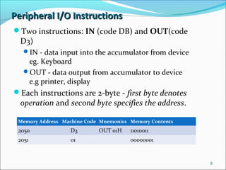
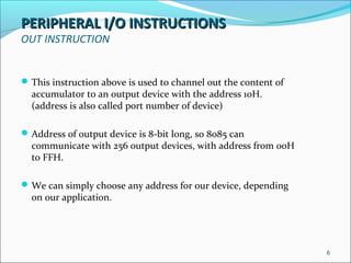
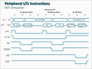
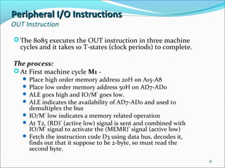
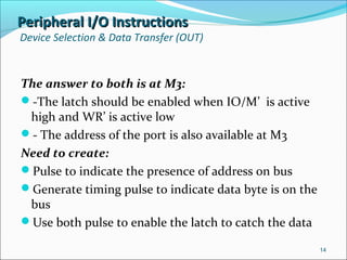
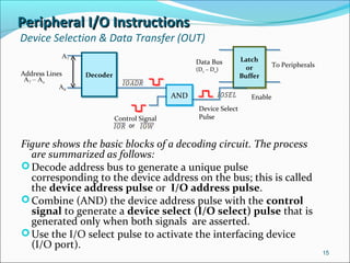
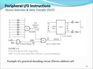
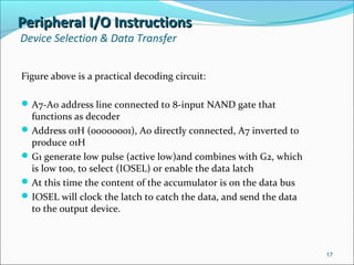
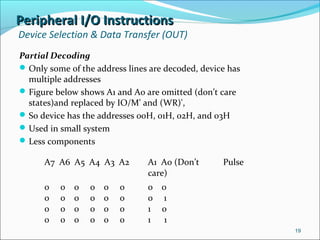
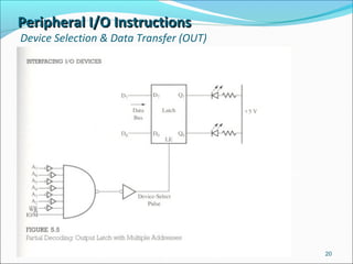
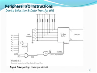
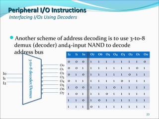
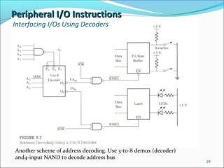
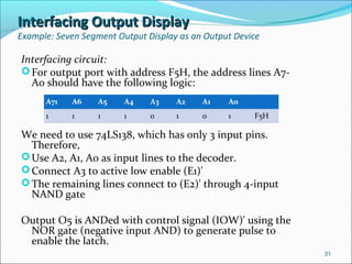
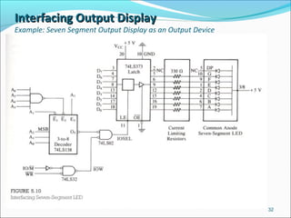
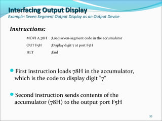
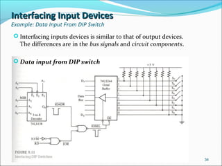
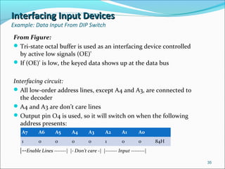
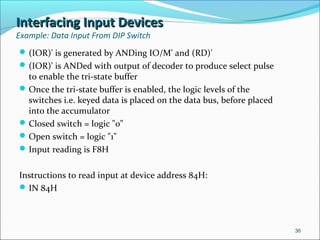
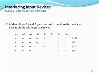
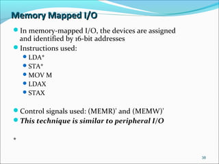
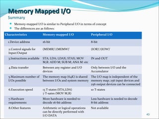
Chapter 5
1
IntroductionIntroduction
Objectives
Parallel and Serial Mode
Identify device/port address of peripheral-mapped I/O and
memory mapped I/O
OUT & IN instructions.
Memory related instructions
Differentiate peripheral-mapped and memory-mapped I/O
To interface 8085 with other devices
Parallel Vs Serial
Parallel I/O - All 8-bits of data are transferred between 8085
and external device using the entire data bus
Serial I/O - Bits are transferred one at a time, along one data
line
2
IntroductionIntroduction
I/O Port Identification and Addressing
 Memory Mapped I/O
 Access and identify as memory registers using memory
space
 Memory related control signal
 16-bit address i.e. from 0000H to FFFFH
 8085 treats I/O ports as if it was communicating with a
memory location
 Peripheral Mapped I/O
 Separate address scheme (8-bit i.e from 00H to FFH)
 Enabled and identified by I/O related control signals
 Data transfer process is identical for both method
 Need to understand the foundation I/O operations in 8085
3
Basic Interfacing ConceptsBasic Interfacing Concepts
8085’s I/O Data Transfer Process:
- Microprocessor place the appropriate address on address
bus
-Send the control signals
-Enable the interfacing device
-Transfer data
Things to understand:
How 8085 selects an I/O device?
What hardware chips are necessary?
What software instructions are used?
How data are transferred?
Peripheral-mapped and memory-mapped I/O have the same
basic concept in interfacing.
The difference is the Instructions used for each.
4
Peripheral I/O InstructionsPeripheral I/O Instructions
Two instructions: IN (code DB) and OUT(code
D3)
IN - data input into the accumulator from device
eg. Keyboard
OUT - data output from accumulator to device
e.g printer, display
Each instructions are 2-byte - first byte denotes
operation and second byte specifies the address.
5
Memory Address Machine Code Mnemonics Memory Contents
2050 D3 OUT 01H 11010011
2051 01 00000001
PERIPHERAL I/O INSTRUCTIONSPERIPHERAL I/O INSTRUCTIONS
OUT INSTRUCTION
This instruction above is used to channel out the content of
accumulator to an output device with the address 10H.
(address is also called port number of device)
Address of output device is 8-bit long, so 8085 can
communicate with 256 output devices, with address from 00H
to FFH.
We can simply choose any address for our device, depending
on our application.
6
Instruction OUT
M1 (Opcode Fetch) M2 (Memory Read) M3 (I/O Write)
T1 T2 T3 T4 T1 T2 T3 T1 T2 T3
Peripheral I/O InstructionsPeripheral I/O Instructions
OUT Instruction
7
20H unspecified 20H Port Address 01H
50H Opcode D3H 51H 01H Port Address
01H
Accumulator
Content
Peripheral I/O InstructionsPeripheral I/O Instructions
OUT Instruction
The 8085 executes the OUT instruction in three machine
cycles and it takes 10 T-states (clock periods) to complete.
The process:
At First machine cycle M1 -
 Place high order memory address 20H on A15-A8
 Place low order memory address 50H on AD7-AD0
 ALE goes high and IO/M' goes low.
 ALE indicates the availability of AD7-AD0 and used to
demultiplex the bus
 IO/M' low indicates a memory related operation
 At T2, (RD)' (active low) signal is sent and combined with
IO/M' signal to activate the (MEMR)' signal (active low)
 Fetch the instruction code D3 using data bus, decodes it,
finds out that it suppose to be 2-byte, so must read the
second byte.
8
Peripheral I/O InstructionsPeripheral I/O Instructions
OUT Instruction
 At the second machine cycle M2 -
 Same process as in M1, but this time with the memory address 2051H
 Gets the device port address 01H, second byte of the OUT
instruction
 At the third machine cycle M3 -
 01H is placed on the low-order (AD7-AD0) and high-order (A15-A8)
address bus
 IO/M' goes high to indicate I/O operation.
 At T2, the content of accumulator is placed on data bus (AD7-AD0),
followed by control signal (WR)’.
 ANDing the IO/M' and (WR)' signal, the (IOW)' is generated to
enable the output device
 The data remains on the data bus (AD7-AD0) for two T-states (T2 & T3),
before the processor executes the next instruction. Therefore we must
latch the data bus within the two T-states before it is lost.
9
Peripheral I/O InstructionsPeripheral I/O Instructions
IN Instruction
IN 8-bit is a two-byte instruction with hex opcode DB followed
by the port address of an input device.
8085 will read the contents of the addresses 2065H and 2066H,
and read the switch positions (input data) at port 84H by
enabling the interfacing device of the port.
Input data byte containing the switch positions from the input
port will be placed in the accumulator.
10
Memory Address Machine Code Mnemonics Memory Contents
2065 DB IN 84H 11011011 (DBH)
2066 84 10000100 (84H)
Peripheral I/O InstructionsPeripheral I/O Instructions
IN Instruction
11
Instruction IN
M1 (Opcode Fetch) M2 (Memory Read) M3 (I/O Write)
T1 T2 T3 T4 T1 T2 T3 T1 T2 T3
20H unspecified Port Address 84H
65H Opcode DBH 66H 84H Port Address
84H
Data From
Input Port
20H
Peripheral I/O InstructionsPeripheral I/O Instructions
IN Instruction
The process:
M1 and M2 are identical to OUT instruction.
At third machine cycle M3 -
8085 places address of input port (84H) on both high-
order AD7-AD0 and low order A15-A8 address bus
Sends (RD)' signal, which will prompt I/O Read signal,
(IOR)'
The (IOR)' enables input port, data obtained from port
onto the bus and placed into the accumulator.
M3 for IN and OUT are essentially the same, the
differences are
 IN use (RD)', OUT use (WR)'
 Data flow from input port to accumulator for IN, from
accumulator to output port for OUT
12
Peripheral I/O InstructionsPeripheral I/O Instructions
Device Selection & Data Transfer (OUT)
We saw that, for OUT instruction, the content of the
accumulator will be on the data bus for a period of two T-
periods only.
To catch the data, we need a data latch so that we can
display or print the data, or even transfer it to an external
device.
Questions:
1. When should we enable the latch?
2. What is the address of the latch?
13
Peripheral I/O InstructionsPeripheral I/O Instructions
Device Selection & Data Transfer (OUT)
The answer to both is at M3:
-The latch should be enabled when IO/M’ is active
high and WR’ is active low
- The address of the port is also available at M3
Need to create:
Pulse to indicate the presence of address on bus
Generate timing pulse to indicate data byte is on the
bus
Use both pulse to enable the latch to catch the data
14
Peripheral I/O InstructionsPeripheral I/O Instructions
Device Selection & Data Transfer (OUT)
Figure shows the basic blocks of a decoding circuit. The process
are summarized as follows:
Decode address bus to generate a unique pulse
corresponding to the device address on the bus; this is called
the device address pulse or I/O address pulse.
Combine (AND) the device address pulse with the control
signal to generate a device select (I/O select) pulse that is
generated only when both signals are asserted.
Use the I/O select pulse to activate the interfacing device
(I/O port).
15
DecoderDecoder
ANDAND
Latch
or
Buffer
Latch
or
BufferAddress Lines
A7 – Ao
A7
A0
or
Control Signal
Device Select
Pulse
Enable
To PeripheralsData Bus
(D7 – D0)
Peripheral I/O InstructionsPeripheral I/O Instructions
Device Selection & Data Transfer (OUT)
16
Example of a practical decoding circuit (Device address 01H)
Peripheral I/O InstructionsPeripheral I/O Instructions
Device Selection & Data Transfer
Figure above is a practical decoding circuit:
A7-A0 address line connected to 8-input NAND gate that
functions as decoder
Address 01H (00000001), A0 directly connected, A7 inverted to
produce 01H
G1 generate low pulse (active low)and combines with G2, which
is low too, to select (IOSEL) or enable the data latch
At this time the content of the accumulator is on the data bus
IOSEL will clock the latch to catch the data, and send the data
to the output device.
17
Peripheral I/O InstructionsPeripheral I/O Instructions
Device Selection & Data Transfer
Absolute Decoding
All eight address lines are decoded to generate
unique pulse
Figure shows unique pulse will be generated if
and only if address 01H (ooooooo1) is on the
address bus
Good design practice
Costly (uses many extra devices/gates)
Our previous decoding circuit employs this
technique
18
Peripheral I/O InstructionsPeripheral I/O Instructions
Device Selection & Data Transfer (OUT)
Partial Decoding
Only some of the address lines are decoded, device has
multiple addresses
Figure below shows A1 and A0 are omitted (don’t care
states)and replaced by IO/M' and (WR)',
So device has the addresses 00H, 01H, 02H, and 03H
Used in small system
Less components
19
A7 A6 A5 A4 A3 A2 A1 A0 (Don’t
care)
Pulse
0 0 0 0 0 0
0 0 0 0 0 0
0 0 0 0 0 0
0 0 0 0 0 0
0 0
0 1
1 0
1 1
Peripheral I/O InstructionsPeripheral I/O Instructions
Device Selection & Data Transfer (OUT)
20
Decoding circuit implemented
using Partial Decoding
technique
Peripheral I/O InstructionsPeripheral I/O Instructions
Device Selection & Data Transfer (IN)
21
Input Interfacing: Example circuit
Peripheral I/O InstructionsPeripheral I/O Instructions
Device Selection & Data Transfer (IN)
Input Interfacing
Example of 8-Key input port. Basic concept is the same as outputBasic concept is the same as output
The process:
 Address line connected to 8-inout NAND gate.
 When address is FFH, NAND out put goes low and combined
with (IOR)' in gate G2
 G2 generate device select pulse used to enable tri-state buffer
 Data from keys are put on the data bus D7-D0 and loaded onto
the accumulator
The difference of this input circuit to the previous output circuit:
 -Control signal IOR is used instead of IOW
 -Tri-state buffer is used an interfacing port instead of latch
 -Data flow is different, e.g from accumulator to leds
22
Peripheral I/O InstructionsPeripheral I/O Instructions
Interfacing I/Os Using Decoders
Another scheme of address decoding is to use 3-to-8
demux (decoder) and4-input NAND to decode
address bus
23
3-to-8decoder/Demux3-to-8decoder/Demux
I0
I1
I2
O0
O1
O2
O3
O4
O5
O6
O7
I2 I1 I0 O7 O6 O5 O4 O3 O2 O1 O0
0 0 0 1 1 1 1 1 1 1 0
0 0 1 1 1 1 1 1 1 0 1
0 1 0 1 1 1 1 1 0 1 1
0 1 1 1 1 1 1 0 1 1 1
1 0 0 1 1 1 0 1 1 1 1
1 0 1 1 1 0 1 1 1 1 1
1 1 0 1 0 1 1 1 1 1 1
1 1 1 0 1 1 1 1 1 1 1
Peripheral I/O InstructionsPeripheral I/O Instructions
Interfacing I/Os Using Decoders
24
Another scheme of address decoding. Use 3-to-8 demux (decoder)
and4-input NAND to decode address bus
Peripheral I/O InstructionsPeripheral I/O Instructions
Interfacing I/Os Using Decoders
This is how the circuit work:
3-to-8 decoder has 3 inputs, 3 enable pins and 8 outputs
For the decoder to be functional, all the enable switches
must be active, i.e. E1' = 0 (active low), E'2 = 0 (active low)
and E'3 = 1 (active high)
Addresses lines A2, A1 and A0 are used as inputs,
therefore we can have 8 different output device or port
addresses. (2^3 = 8)
A7-A3 are used to enable the encoder
Combine the decoded signal with the appropriate control
signal to generate I/O select pulse
Here, O0 is logically ANDed with (IOW)' signal to select
the output port for output operation
O2 is logically NAND with (IOR)' to select the tri-state
buffer for input operation
25
Peripheral I/O InstructionsPeripheral I/O Instructions
Interfacing I/Os Using Decoders
Decoder Enable
A7 A6 A5 A4 A3
Input
A2 A1 A0
Address
1 1 1 1 1 0 0 0 F84H
Based on the circuit, select pulse will be generated if
input address is F8H, where O0 will be active and
LED will display the content of accumulator
Select pulse will also be generated if input address is
FAH, where O2 will be active in this case and the
buffer will channel the keyed data into the
accumulator
26
Peripheral I/O InstructionsPeripheral I/O Instructions
Basic Interfacing Concept Summary
Basic concepts and steps for peripheral I/O interfacing:
The device address or port number is placed on the
demultiplexed low order as well as high order address bus
 Either the high order bus (A15-A8) or the demultiplexed
low order bus (A7-A0) can be decoded to generate the
pulse that correspond to the device address
Device address is AND with either the (IOW)' for output or
(IOR)' for input control signal. When both is active, the
device I/O device will be selected
Output device, Latch is used
Input device, tri-state buffer is used
Address bus can be decoded by Absolute or Partial (liner-
select)decoding. Partial technique reduces cost and
components, but device has multiple addresses.
27
Peripheral I/O InstructionsPeripheral I/O Instructions
Basic Interfacing Concept Summary
 8085’s I/O Data Transfer Process:
 Places appropriate address on the address bus
 Sends the control signals
 Enables the interfacing device
 Transfer data
Interesting Question:
Can an input port and an output port have the same port address?
Answer:
Another Interesting Question:
How will the port number be affected if we decode the high-order
address lines A15-A8 rather than A7-A0?
Answer:
28
Interfacing Output DisplayInterfacing Output Display
Example: Seven Segment Output Display as an Output Device
Problem:
Design a seven-segment LED output port with the device
address F5H, using a 74LS138 (3-to-8) decoder, a 74LS20 4-
input NAND gate, a 74LS02 NOR gate, and a common-anode
seven-segment LED
Write instructions to display digit 7 at the port
29
Interfacing Output DisplayInterfacing Output Display
Example: Seven Segment Output Display as an Output Device
Solution:
Seven-Segment LED
To display digit "7" at the LED as in figure, the requirements are:
Logic "0" is required to turn on a segment because it is a
common-anode seven-segment LED
To display "7", segments A, B, and C should be turned on
The binary code should be:
30
Data Lines D7 D6 D5 D4 D3 D2 D1 D0
Bits 1 1 1 1 1 0 0 0 78H
Segments NC G F E D C B A
Interfacing Output DisplayInterfacing Output Display
Example: Seven Segment Output Display as an Output Device
Interfacing circuit:
For output port with address F5H, the address lines A7-
A0 should have the following logic:
We need to use 74LS138, which has only 3 input pins.
Therefore,
Use A2, A1, A0 as input lines to the decoder.
Connect A3 to active low enable (E1)'
The remaining lines connect to (E2)' through 4-input
NAND gate
Output O5 is ANDed with control signal (IOW)' using the
NOR gate (negative input AND) to generate pulse to
enable the latch.
31
A71 A6 A5 A4 A3 A2 A1 A0
1 1 1 1 0 1 0 1 F5H
Interfacing Output DisplayInterfacing Output Display
Example: Seven Segment Output Display as an Output Device
32
Interfacing Output DisplayInterfacing Output Display
Example: Seven Segment Output Display as an Output Device
Instructions:
First instruction loads 78H in the accumulator,
which is the code to display digit "7“
Second instruction sends contents of the
accumulator (78H) to the output port F5H
33
MOVI A,78H ;Load seven-segment code in the accumulator
OUT F5H ;Display digit 7 at port F5H
HLT ;End
Interfacing Input DevicesInterfacing Input Devices
Example: Data Input From DIP Switch
 Interfacing inputs devices is similar to that of output devices.
The differences are in the bus signals and circuit components.
 Data input from DIP switch
34
Interfacing Input DevicesInterfacing Input Devices
Example: Data Input From DIP Switch
From Figure:
Tri-state octal buffer is used as an interfacing device controlled
by active low signals (OE)'
If (OE)' is low, the keyed data shows up at the data bus
Interfacing circuit:
All low-order address lines, except A4 and A3, are connected to
the decoder
A4 and A3 are don’t care lines
Output pin O4 is used, so it will switch on when the following
address presents:
|--Enable Lines -------| |- Don’t care -| |------- Input --------|
35
A7 A6 A5 A4 A3 A2 A1 A0  
1 0 0 0 0 1 0 0 84H
Interfacing Input DevicesInterfacing Input Devices
Example: Data Input From DIP Switch
(IOR)' is generated by ANDing IO/M' and (RD)'
(IOR)' is ANDed with output of decoder to produce select pulse
to enable the tri-state buffer
Once the tri-state buffer is enabled, the logic levels of the
switches i.e. keyed data is placed on the data bus, before placed
into the accumulator
Closed switch = logic "0"
Open switch = logic "1"
Input reading is F8H
Instructions to read input at device address 84H:
IN 84H
36
Interfacing Input DevicesInterfacing Input Devices
Example: Data Input From DIP Switch
Address lines A4 and A3 are not used, therefore the device can
have multiple addresses as shown:
37
A7 A6 A5 A4 A3 A2 A1 A0
1 0 0 0 0 1 0 0 84 H
1 0 0 0 1 1 0 0 8CH
1 0 0 1 0 1 0 0 94H
1 0 0 1 1 1 0 0 9CH
Memory Mapped I/OMemory Mapped I/O
In memory-mapped I/O, the devices are assigned
and identified by 16-bit addresses
Instructions used:
LDA*
STA*
MOV M
LDAX
STAX
Control signals used: (MEMR)' and (MEMW)'
This technique is similar to peripheral I/O
* -
38
Memory Mapped I/OMemory Mapped I/O
STA (Store A Direct) is used to store the content
of accumulator to the specified memory register.
Here the memory address is 8000H (16-bit)
If we connect an output device with this address
(8000H), the accumulator contents will transfer
to the output device.
39
Memory Address Machine Code Mnemonics Comments
2050 32 STA 8000H ; Store Contents of
accumulator in memory
location 8000H
2051 00
2052 80
Memory Mapped I/OMemory Mapped I/O
For input operation, same principles as output
operation
Use LDA (Load A Direct) instead of STA
For memory-mapped I/O, the control signals are
memory read (MEMR)' and memory write
(MEMW)' instead of (IOR)' and (IOW)'
40
Memory Mapped I/OMemory Mapped I/O
Data Transfer Instructions
 Essentially the same as using IN and Out instructions
 But memory-mapped uses 16-bit addressing, therefore needs
4 machine cycles, instead of 3 as in the time diagram
 M1 is for reading Opcode (first byte of instruction)
 M2 is for reading 2nd byte of instruction, which is the low
order address
 M3 is for rading 3rd byte of instruction, which is the remaining
high order address
 M4, data are loaded from the accumulator to the data bus and
address 8000H are put on the entire address bus (A15-A0)
 We can see the difference here. For OUT instruction, the 8-bit
address of device is put on both the A15-A8 and A7-A0 address
bus, and either one can be decoded to identify the output
device
 For memory mapped, all the 16 address lines need to be
decoded to identify the output device
41
Memory Mapped I/OMemory Mapped I/O
Data Transfer Instructions
The steps for device selection and data transfer for
memory-mapped I/O:
1. Decode the address bus to generate the device
address pulse
2. AND the control signal with the device address
pulse to generate the device select (I/O select) pulse
3. Use the device select pulse to enable the I/O port
For interfacing memory-mapped input device, we can
use the similar steps, but use the instruction LDA,
and the control signal will be (RD)' rather than
(WR)'
42
Memory Mapped I/OMemory Mapped I/O
Summary
 Memory-mapped I/O is similar to Peripheral I/O in terms of concept
 The differences are as follows:
43
Characteristics Memory-mapped I/O Peripheral I/O
1.Device address 16-bit 8-bit
2.Control signals for
Input/Output
(MEMR)'/(MEMW)' (IOR)'/(IOW)'
3.Instructions available STA; LDA; LDAX; STAX; MOV
M,R: ADD M; SUB M; ANA M: etc
IN and OUT
4.Data transfer Between any register and I/O
devices
Only between I/O and the
Accumulator
5.Maximum number of
I/Os possible
The memory map (64K) is shared
between I/Os and system memory
The I/O map is independent of the
memory map; 256 input devices and
256 output devices can be connected
6.Execution speed 13 T-states (STA,LDA)
7 T-sates (MOV M,R)
10 T-states
7.Hardware
requirements
More hardware is needed to
decode 16-bit address
Less hardware is needed to decode
8-bit address
8.Other features Arithmetic or logical operations
can be directly performed with
I/O DATA
Not available

Chapter 5

  • 1.
  • 2.
    IntroductionIntroduction Objectives Parallel and SerialMode Identify device/port address of peripheral-mapped I/O and memory mapped I/O OUT & IN instructions. Memory related instructions Differentiate peripheral-mapped and memory-mapped I/O To interface 8085 with other devices Parallel Vs Serial Parallel I/O - All 8-bits of data are transferred between 8085 and external device using the entire data bus Serial I/O - Bits are transferred one at a time, along one data line 2
  • 3.
    IntroductionIntroduction I/O Port Identificationand Addressing  Memory Mapped I/O  Access and identify as memory registers using memory space  Memory related control signal  16-bit address i.e. from 0000H to FFFFH  8085 treats I/O ports as if it was communicating with a memory location  Peripheral Mapped I/O  Separate address scheme (8-bit i.e from 00H to FFH)  Enabled and identified by I/O related control signals  Data transfer process is identical for both method  Need to understand the foundation I/O operations in 8085 3
  • 4.
    Basic Interfacing ConceptsBasicInterfacing Concepts 8085’s I/O Data Transfer Process: - Microprocessor place the appropriate address on address bus -Send the control signals -Enable the interfacing device -Transfer data Things to understand: How 8085 selects an I/O device? What hardware chips are necessary? What software instructions are used? How data are transferred? Peripheral-mapped and memory-mapped I/O have the same basic concept in interfacing. The difference is the Instructions used for each. 4
  • 5.
    Peripheral I/O InstructionsPeripheralI/O Instructions Two instructions: IN (code DB) and OUT(code D3) IN - data input into the accumulator from device eg. Keyboard OUT - data output from accumulator to device e.g printer, display Each instructions are 2-byte - first byte denotes operation and second byte specifies the address. 5 Memory Address Machine Code Mnemonics Memory Contents 2050 D3 OUT 01H 11010011 2051 01 00000001
  • 6.
    PERIPHERAL I/O INSTRUCTIONSPERIPHERALI/O INSTRUCTIONS OUT INSTRUCTION This instruction above is used to channel out the content of accumulator to an output device with the address 10H. (address is also called port number of device) Address of output device is 8-bit long, so 8085 can communicate with 256 output devices, with address from 00H to FFH. We can simply choose any address for our device, depending on our application. 6
  • 7.
    Instruction OUT M1 (OpcodeFetch) M2 (Memory Read) M3 (I/O Write) T1 T2 T3 T4 T1 T2 T3 T1 T2 T3 Peripheral I/O InstructionsPeripheral I/O Instructions OUT Instruction 7 20H unspecified 20H Port Address 01H 50H Opcode D3H 51H 01H Port Address 01H Accumulator Content
  • 8.
    Peripheral I/O InstructionsPeripheralI/O Instructions OUT Instruction The 8085 executes the OUT instruction in three machine cycles and it takes 10 T-states (clock periods) to complete. The process: At First machine cycle M1 -  Place high order memory address 20H on A15-A8  Place low order memory address 50H on AD7-AD0  ALE goes high and IO/M' goes low.  ALE indicates the availability of AD7-AD0 and used to demultiplex the bus  IO/M' low indicates a memory related operation  At T2, (RD)' (active low) signal is sent and combined with IO/M' signal to activate the (MEMR)' signal (active low)  Fetch the instruction code D3 using data bus, decodes it, finds out that it suppose to be 2-byte, so must read the second byte. 8
  • 9.
    Peripheral I/O InstructionsPeripheralI/O Instructions OUT Instruction  At the second machine cycle M2 -  Same process as in M1, but this time with the memory address 2051H  Gets the device port address 01H, second byte of the OUT instruction  At the third machine cycle M3 -  01H is placed on the low-order (AD7-AD0) and high-order (A15-A8) address bus  IO/M' goes high to indicate I/O operation.  At T2, the content of accumulator is placed on data bus (AD7-AD0), followed by control signal (WR)’.  ANDing the IO/M' and (WR)' signal, the (IOW)' is generated to enable the output device  The data remains on the data bus (AD7-AD0) for two T-states (T2 & T3), before the processor executes the next instruction. Therefore we must latch the data bus within the two T-states before it is lost. 9
  • 10.
    Peripheral I/O InstructionsPeripheralI/O Instructions IN Instruction IN 8-bit is a two-byte instruction with hex opcode DB followed by the port address of an input device. 8085 will read the contents of the addresses 2065H and 2066H, and read the switch positions (input data) at port 84H by enabling the interfacing device of the port. Input data byte containing the switch positions from the input port will be placed in the accumulator. 10 Memory Address Machine Code Mnemonics Memory Contents 2065 DB IN 84H 11011011 (DBH) 2066 84 10000100 (84H)
  • 11.
    Peripheral I/O InstructionsPeripheralI/O Instructions IN Instruction 11 Instruction IN M1 (Opcode Fetch) M2 (Memory Read) M3 (I/O Write) T1 T2 T3 T4 T1 T2 T3 T1 T2 T3 20H unspecified Port Address 84H 65H Opcode DBH 66H 84H Port Address 84H Data From Input Port 20H
  • 12.
    Peripheral I/O InstructionsPeripheralI/O Instructions IN Instruction The process: M1 and M2 are identical to OUT instruction. At third machine cycle M3 - 8085 places address of input port (84H) on both high- order AD7-AD0 and low order A15-A8 address bus Sends (RD)' signal, which will prompt I/O Read signal, (IOR)' The (IOR)' enables input port, data obtained from port onto the bus and placed into the accumulator. M3 for IN and OUT are essentially the same, the differences are  IN use (RD)', OUT use (WR)'  Data flow from input port to accumulator for IN, from accumulator to output port for OUT 12
  • 13.
    Peripheral I/O InstructionsPeripheralI/O Instructions Device Selection & Data Transfer (OUT) We saw that, for OUT instruction, the content of the accumulator will be on the data bus for a period of two T- periods only. To catch the data, we need a data latch so that we can display or print the data, or even transfer it to an external device. Questions: 1. When should we enable the latch? 2. What is the address of the latch? 13
  • 14.
    Peripheral I/O InstructionsPeripheralI/O Instructions Device Selection & Data Transfer (OUT) The answer to both is at M3: -The latch should be enabled when IO/M’ is active high and WR’ is active low - The address of the port is also available at M3 Need to create: Pulse to indicate the presence of address on bus Generate timing pulse to indicate data byte is on the bus Use both pulse to enable the latch to catch the data 14
  • 15.
    Peripheral I/O InstructionsPeripheralI/O Instructions Device Selection & Data Transfer (OUT) Figure shows the basic blocks of a decoding circuit. The process are summarized as follows: Decode address bus to generate a unique pulse corresponding to the device address on the bus; this is called the device address pulse or I/O address pulse. Combine (AND) the device address pulse with the control signal to generate a device select (I/O select) pulse that is generated only when both signals are asserted. Use the I/O select pulse to activate the interfacing device (I/O port). 15 DecoderDecoder ANDAND Latch or Buffer Latch or BufferAddress Lines A7 – Ao A7 A0 or Control Signal Device Select Pulse Enable To PeripheralsData Bus (D7 – D0)
  • 16.
    Peripheral I/O InstructionsPeripheralI/O Instructions Device Selection & Data Transfer (OUT) 16 Example of a practical decoding circuit (Device address 01H)
  • 17.
    Peripheral I/O InstructionsPeripheralI/O Instructions Device Selection & Data Transfer Figure above is a practical decoding circuit: A7-A0 address line connected to 8-input NAND gate that functions as decoder Address 01H (00000001), A0 directly connected, A7 inverted to produce 01H G1 generate low pulse (active low)and combines with G2, which is low too, to select (IOSEL) or enable the data latch At this time the content of the accumulator is on the data bus IOSEL will clock the latch to catch the data, and send the data to the output device. 17
  • 18.
    Peripheral I/O InstructionsPeripheralI/O Instructions Device Selection & Data Transfer Absolute Decoding All eight address lines are decoded to generate unique pulse Figure shows unique pulse will be generated if and only if address 01H (ooooooo1) is on the address bus Good design practice Costly (uses many extra devices/gates) Our previous decoding circuit employs this technique 18
  • 19.
    Peripheral I/O InstructionsPeripheralI/O Instructions Device Selection & Data Transfer (OUT) Partial Decoding Only some of the address lines are decoded, device has multiple addresses Figure below shows A1 and A0 are omitted (don’t care states)and replaced by IO/M' and (WR)', So device has the addresses 00H, 01H, 02H, and 03H Used in small system Less components 19 A7 A6 A5 A4 A3 A2 A1 A0 (Don’t care) Pulse 0 0 0 0 0 0 0 0 0 0 0 0 0 0 0 0 0 0 0 0 0 0 0 0 0 0 0 1 1 0 1 1
  • 20.
    Peripheral I/O InstructionsPeripheralI/O Instructions Device Selection & Data Transfer (OUT) 20 Decoding circuit implemented using Partial Decoding technique
  • 21.
    Peripheral I/O InstructionsPeripheralI/O Instructions Device Selection & Data Transfer (IN) 21 Input Interfacing: Example circuit
  • 22.
    Peripheral I/O InstructionsPeripheralI/O Instructions Device Selection & Data Transfer (IN) Input Interfacing Example of 8-Key input port. Basic concept is the same as outputBasic concept is the same as output The process:  Address line connected to 8-inout NAND gate.  When address is FFH, NAND out put goes low and combined with (IOR)' in gate G2  G2 generate device select pulse used to enable tri-state buffer  Data from keys are put on the data bus D7-D0 and loaded onto the accumulator The difference of this input circuit to the previous output circuit:  -Control signal IOR is used instead of IOW  -Tri-state buffer is used an interfacing port instead of latch  -Data flow is different, e.g from accumulator to leds 22
  • 23.
    Peripheral I/O InstructionsPeripheralI/O Instructions Interfacing I/Os Using Decoders Another scheme of address decoding is to use 3-to-8 demux (decoder) and4-input NAND to decode address bus 23 3-to-8decoder/Demux3-to-8decoder/Demux I0 I1 I2 O0 O1 O2 O3 O4 O5 O6 O7 I2 I1 I0 O7 O6 O5 O4 O3 O2 O1 O0 0 0 0 1 1 1 1 1 1 1 0 0 0 1 1 1 1 1 1 1 0 1 0 1 0 1 1 1 1 1 0 1 1 0 1 1 1 1 1 1 0 1 1 1 1 0 0 1 1 1 0 1 1 1 1 1 0 1 1 1 0 1 1 1 1 1 1 1 0 1 0 1 1 1 1 1 1 1 1 1 0 1 1 1 1 1 1 1
  • 24.
    Peripheral I/O InstructionsPeripheralI/O Instructions Interfacing I/Os Using Decoders 24 Another scheme of address decoding. Use 3-to-8 demux (decoder) and4-input NAND to decode address bus
  • 25.
    Peripheral I/O InstructionsPeripheralI/O Instructions Interfacing I/Os Using Decoders This is how the circuit work: 3-to-8 decoder has 3 inputs, 3 enable pins and 8 outputs For the decoder to be functional, all the enable switches must be active, i.e. E1' = 0 (active low), E'2 = 0 (active low) and E'3 = 1 (active high) Addresses lines A2, A1 and A0 are used as inputs, therefore we can have 8 different output device or port addresses. (2^3 = 8) A7-A3 are used to enable the encoder Combine the decoded signal with the appropriate control signal to generate I/O select pulse Here, O0 is logically ANDed with (IOW)' signal to select the output port for output operation O2 is logically NAND with (IOR)' to select the tri-state buffer for input operation 25
  • 26.
    Peripheral I/O InstructionsPeripheralI/O Instructions Interfacing I/Os Using Decoders Decoder Enable A7 A6 A5 A4 A3 Input A2 A1 A0 Address 1 1 1 1 1 0 0 0 F84H Based on the circuit, select pulse will be generated if input address is F8H, where O0 will be active and LED will display the content of accumulator Select pulse will also be generated if input address is FAH, where O2 will be active in this case and the buffer will channel the keyed data into the accumulator 26
  • 27.
    Peripheral I/O InstructionsPeripheralI/O Instructions Basic Interfacing Concept Summary Basic concepts and steps for peripheral I/O interfacing: The device address or port number is placed on the demultiplexed low order as well as high order address bus  Either the high order bus (A15-A8) or the demultiplexed low order bus (A7-A0) can be decoded to generate the pulse that correspond to the device address Device address is AND with either the (IOW)' for output or (IOR)' for input control signal. When both is active, the device I/O device will be selected Output device, Latch is used Input device, tri-state buffer is used Address bus can be decoded by Absolute or Partial (liner- select)decoding. Partial technique reduces cost and components, but device has multiple addresses. 27
  • 28.
    Peripheral I/O InstructionsPeripheralI/O Instructions Basic Interfacing Concept Summary  8085’s I/O Data Transfer Process:  Places appropriate address on the address bus  Sends the control signals  Enables the interfacing device  Transfer data Interesting Question: Can an input port and an output port have the same port address? Answer: Another Interesting Question: How will the port number be affected if we decode the high-order address lines A15-A8 rather than A7-A0? Answer: 28
  • 29.
    Interfacing Output DisplayInterfacingOutput Display Example: Seven Segment Output Display as an Output Device Problem: Design a seven-segment LED output port with the device address F5H, using a 74LS138 (3-to-8) decoder, a 74LS20 4- input NAND gate, a 74LS02 NOR gate, and a common-anode seven-segment LED Write instructions to display digit 7 at the port 29
  • 30.
    Interfacing Output DisplayInterfacingOutput Display Example: Seven Segment Output Display as an Output Device Solution: Seven-Segment LED To display digit "7" at the LED as in figure, the requirements are: Logic "0" is required to turn on a segment because it is a common-anode seven-segment LED To display "7", segments A, B, and C should be turned on The binary code should be: 30 Data Lines D7 D6 D5 D4 D3 D2 D1 D0 Bits 1 1 1 1 1 0 0 0 78H Segments NC G F E D C B A
  • 31.
    Interfacing Output DisplayInterfacingOutput Display Example: Seven Segment Output Display as an Output Device Interfacing circuit: For output port with address F5H, the address lines A7- A0 should have the following logic: We need to use 74LS138, which has only 3 input pins. Therefore, Use A2, A1, A0 as input lines to the decoder. Connect A3 to active low enable (E1)' The remaining lines connect to (E2)' through 4-input NAND gate Output O5 is ANDed with control signal (IOW)' using the NOR gate (negative input AND) to generate pulse to enable the latch. 31 A71 A6 A5 A4 A3 A2 A1 A0 1 1 1 1 0 1 0 1 F5H
  • 32.
    Interfacing Output DisplayInterfacingOutput Display Example: Seven Segment Output Display as an Output Device 32
  • 33.
    Interfacing Output DisplayInterfacingOutput Display Example: Seven Segment Output Display as an Output Device Instructions: First instruction loads 78H in the accumulator, which is the code to display digit "7“ Second instruction sends contents of the accumulator (78H) to the output port F5H 33 MOVI A,78H ;Load seven-segment code in the accumulator OUT F5H ;Display digit 7 at port F5H HLT ;End
  • 34.
    Interfacing Input DevicesInterfacingInput Devices Example: Data Input From DIP Switch  Interfacing inputs devices is similar to that of output devices. The differences are in the bus signals and circuit components.  Data input from DIP switch 34
  • 35.
    Interfacing Input DevicesInterfacingInput Devices Example: Data Input From DIP Switch From Figure: Tri-state octal buffer is used as an interfacing device controlled by active low signals (OE)' If (OE)' is low, the keyed data shows up at the data bus Interfacing circuit: All low-order address lines, except A4 and A3, are connected to the decoder A4 and A3 are don’t care lines Output pin O4 is used, so it will switch on when the following address presents: |--Enable Lines -------| |- Don’t care -| |------- Input --------| 35 A7 A6 A5 A4 A3 A2 A1 A0   1 0 0 0 0 1 0 0 84H
  • 36.
    Interfacing Input DevicesInterfacingInput Devices Example: Data Input From DIP Switch (IOR)' is generated by ANDing IO/M' and (RD)' (IOR)' is ANDed with output of decoder to produce select pulse to enable the tri-state buffer Once the tri-state buffer is enabled, the logic levels of the switches i.e. keyed data is placed on the data bus, before placed into the accumulator Closed switch = logic "0" Open switch = logic "1" Input reading is F8H Instructions to read input at device address 84H: IN 84H 36
  • 37.
    Interfacing Input DevicesInterfacingInput Devices Example: Data Input From DIP Switch Address lines A4 and A3 are not used, therefore the device can have multiple addresses as shown: 37 A7 A6 A5 A4 A3 A2 A1 A0 1 0 0 0 0 1 0 0 84 H 1 0 0 0 1 1 0 0 8CH 1 0 0 1 0 1 0 0 94H 1 0 0 1 1 1 0 0 9CH
  • 38.
    Memory Mapped I/OMemoryMapped I/O In memory-mapped I/O, the devices are assigned and identified by 16-bit addresses Instructions used: LDA* STA* MOV M LDAX STAX Control signals used: (MEMR)' and (MEMW)' This technique is similar to peripheral I/O * - 38
  • 39.
    Memory Mapped I/OMemoryMapped I/O STA (Store A Direct) is used to store the content of accumulator to the specified memory register. Here the memory address is 8000H (16-bit) If we connect an output device with this address (8000H), the accumulator contents will transfer to the output device. 39 Memory Address Machine Code Mnemonics Comments 2050 32 STA 8000H ; Store Contents of accumulator in memory location 8000H 2051 00 2052 80
  • 40.
    Memory Mapped I/OMemoryMapped I/O For input operation, same principles as output operation Use LDA (Load A Direct) instead of STA For memory-mapped I/O, the control signals are memory read (MEMR)' and memory write (MEMW)' instead of (IOR)' and (IOW)' 40
  • 41.
    Memory Mapped I/OMemoryMapped I/O Data Transfer Instructions  Essentially the same as using IN and Out instructions  But memory-mapped uses 16-bit addressing, therefore needs 4 machine cycles, instead of 3 as in the time diagram  M1 is for reading Opcode (first byte of instruction)  M2 is for reading 2nd byte of instruction, which is the low order address  M3 is for rading 3rd byte of instruction, which is the remaining high order address  M4, data are loaded from the accumulator to the data bus and address 8000H are put on the entire address bus (A15-A0)  We can see the difference here. For OUT instruction, the 8-bit address of device is put on both the A15-A8 and A7-A0 address bus, and either one can be decoded to identify the output device  For memory mapped, all the 16 address lines need to be decoded to identify the output device 41
  • 42.
    Memory Mapped I/OMemoryMapped I/O Data Transfer Instructions The steps for device selection and data transfer for memory-mapped I/O: 1. Decode the address bus to generate the device address pulse 2. AND the control signal with the device address pulse to generate the device select (I/O select) pulse 3. Use the device select pulse to enable the I/O port For interfacing memory-mapped input device, we can use the similar steps, but use the instruction LDA, and the control signal will be (RD)' rather than (WR)' 42
  • 43.
    Memory Mapped I/OMemoryMapped I/O Summary  Memory-mapped I/O is similar to Peripheral I/O in terms of concept  The differences are as follows: 43 Characteristics Memory-mapped I/O Peripheral I/O 1.Device address 16-bit 8-bit 2.Control signals for Input/Output (MEMR)'/(MEMW)' (IOR)'/(IOW)' 3.Instructions available STA; LDA; LDAX; STAX; MOV M,R: ADD M; SUB M; ANA M: etc IN and OUT 4.Data transfer Between any register and I/O devices Only between I/O and the Accumulator 5.Maximum number of I/Os possible The memory map (64K) is shared between I/Os and system memory The I/O map is independent of the memory map; 256 input devices and 256 output devices can be connected 6.Execution speed 13 T-states (STA,LDA) 7 T-sates (MOV M,R) 10 T-states 7.Hardware requirements More hardware is needed to decode 16-bit address Less hardware is needed to decode 8-bit address 8.Other features Arithmetic or logical operations can be directly performed with I/O DATA Not available