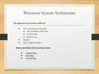
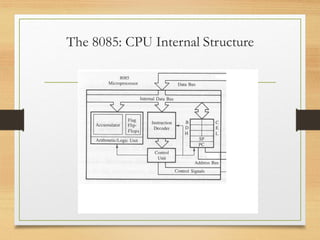
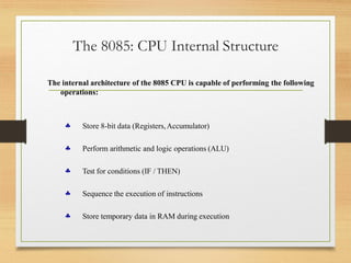
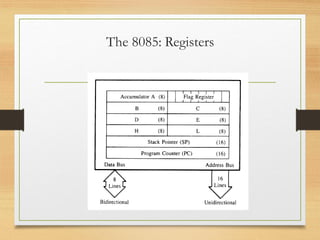
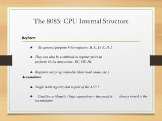
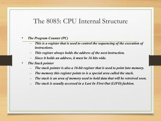
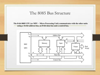
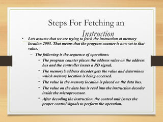
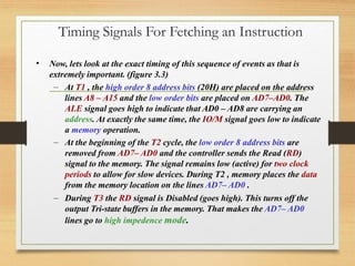
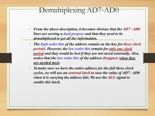
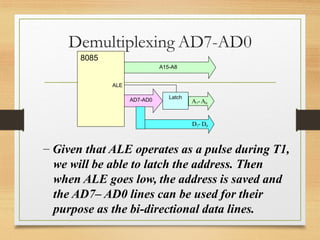
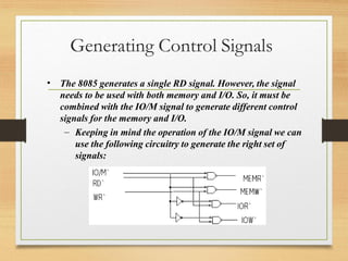
SlideShare a Scribd company logo
1 of 24
Download to read offline
BEE603 - Microprocessor and
Microcontroller
Compiled by,
Mr.K.Dwarakesh
Assistant Professor
Dept. of EEE
BIHER
The typical processor system consists of:
 CPU (central processing unit)



ALU (arithmetic-logic unit)
Control Logic
Registers, etc…


Memory
Input / Output interfaces
Processor System Architecture
Interconnections between these units:



Address Bus
Data Bus
Control Bus
The 8085: CPU Internal Structure
The internal architecture of the 8085 CPU is capable of performing the following
operations:
 Store 8-bit data (Registers,Accumulator)
 Perform arithmetic and logic operations (ALU)
 Test for conditions (IF / THEN)
 Sequence the execution of instructions
 Store temporary data in RAM during execution
The 8085: CPU Internal Structure
The 8085: Registers
Registers
 Six general purpose 8-bit registers: B, C, D, E, H, L
 They can also be combined as register pairs to
perform 16-bit operations: BC, DE, HL
 Registers are programmable (data load, move, etc.)
Accumulator
 Single 8-bit register that is part of the ALU !
 always stored in the
Used for arithmetic / logic operations – the result is
accumulator.
The 8085: CPU Internal Structure
• The Program Counter (PC)
– This is a register that is used to control the sequencing of the execution of
instructions.
– This register always holds the address of the next instruction.
– Since it holds an address, it must be 16 bits wide.
• The Stack pointer
–
–
–
–
The stack pointer is also a 16-bit register that is used to point into memory.
The memory this register points to is a special area called the stack.
The stack is an area of memory used to hold data that will be retreived soon.
The stack is usually accessed in a Last In First Out (LIFO) fashion.
The 8085: CPU Internal Structure
The 8085 and Its Busses
•
•
The 8085 is an 8-bit general purpose microprocessor that can
address 64K Byte of memory.
It has 40 pins and uses +5V for power. It can run at a maximum
frequency of 3 MHz.
– The pins on the chip can be grouped into 6 groups:
• Address Bus.
• Data Bus.
• Control and Status Signals.
• Power supply and frequency.
• Externally Initiated Signals.
• Serial I/O ports.
The 8085 Bus Structure
The 8-bit 8085 CPU (or MPU – Micro Processing Unit) communicates with the other units
using a 16-bit address bus, an 8-bit data bus and a control bus.
The Address and Data Busses
• The address bus has 8 signal lines A8 – A15 which
are unidirectional.
• The other 8 address bits are multiplexed (time shared) with
the 8 data bits.
– So, the bits AD0 – AD7 are bi-directional and serve as
A0 – A7 and D0 – D7 at the same time.
• During the execution of the instruction, these
lines carry the address bits during the early part,
then during the late parts of the execution, they
carry the 8 data bits.
– In order to separate the address from the data, we can
use a latch to save the value before the function of the bits
•
•
The Control and Status Signals
• There are 4 main control and status signals. These are:
• ALE: Address Latch Enable. This signal is a pulse that
become 1 when the AD0 – AD7 lines have an address on
them. It becomes 0 after that. This signal can be used to
enable a latch to save the address bits from the AD lines.
• RD: Read. Active low.
• WR: Write. Active low.
• IO/M: This signal specifies whether the operation is a
memory operation (IO/M=0) or an I/O operation
(IO/M=1).
• S1 and S0 : Status signals to specify the kind of
operation being performed .Usually un-used in small
systems.
Frequency Control Signals
• There are 3 important pins in the frequency control group.
– X0 and X1 are the inputs from the crystal or clock generating
circuit.
• The frequency is internally divided by 2.
– So, to run the microprocessor at 3 MHz, a clock running
at 6 MHz should be connected to the X0 and X1 pins.
– CLK (OUT): An output clock pin to drive the clock of the rest of the
system.
• We will discuss the rest of the control signals as we get to them.
Microprocessor Communication and Bus Timing
• To understand how the microprocessor operates and uses
these different signals, we should study the process of communication
between the microprocessor and memory during a memory read or write
operation.
• Lets look at timing and the data flow of an instruction
fetch operation. (Example 3.1)
•
•
Steps For Fetching an
Instruction
• Lets assume that we are trying to fetch the instruction at memory
location 2005. That means that the program counter is now set to that
value.
– The following is the sequence of operations:
•
•
•
•
• The program counter places the address value on the address
bus and the controller issues a RD signal.
The memory’s address decoder gets the value and determines
which memory location is being accessed.
The value in the memory location is placed on the data bus.
The value on the data bus is read into the instruction decoder
inside the microprocessor.
After decoding the instruction, the control unit issues the
proper control signals to perform the operation.
Timing Signals For Fetching an Instruction
• Now, lets look at the exact timing of this sequence of events as that is
extremely important. (figure 3.3)
–
–
– At T1 , the high order 8 address bits (20H) are placed on the address
lines A8 – A15 and the low order bits are placed on AD7–AD0. The
ALE signal goes high to indicate that AD0 – AD8 are carrying an
address. At exactly the same time, the IO/M signal goes low to indicate
a memory operation.
At the beginning of the T2 cycle, the low order 8 address bits are
removed from AD7– AD0 and the controller sends the Read (RD)
signal to the memory. The signal remains low (active) for two clock
periods to allow for slow devices. During T2 , memory places the data
from the memory location on the lines AD7– AD0 .
During T3 the RD signal is Disabled (goes high). This turns off the
output Tri-state buffers in the memory. That makes the AD7– AD0
lines go to high impedence mode.
Demultiplexing AD7-AD0
–
–
–
From the above description, it becomes obvious that the AD7– AD0
lines are serving a dual purpose and that they need to be
demultiplexed to get all the information.
The high order bits of the address remain on the bus for three clock
periods. However, the low order bits remain for only one clock
period and they would be lost if they are not saved externally. Also,
notice that the low order bits of the address disappear when they
are needed most.
To make sure we have the entire address for the full three clock
cycles, we will use an external latch to save the value of AD7– AD0
when it is carrying the address bits. We use the ALE signal to
enable this latch.
Demultiplexing AD7-AD0
– Given that ALE operates as a pulse during T1,
we will be able to latch the address. Then
when ALE goes low, the address is saved and
the AD7– AD0 lines can be used for their
purpose as the bi-directional data lines.
A15-A8
Latch
AD7-AD0
D7- D0
A7-A0
8085
ALE
Generating Control Signals
• The 8085 generates a single RD signal. However, the signal
needs to be used with both memory and I/O. So, it must be
combined with the IO/M signal to generate different control
signals for the memory and I/O.
– Keeping in mind the operation of the IO/M signal we can
use the following circuitry to generate the right set of
signals:
A closer look at the 8085
Architecture
• Previously we discussed the 8085
from a programmer’s perspective.
• Now, lets look at some of its
features with more detail.
The ALU
• In addition to the arithmetic & logic circuits, the ALU
includes the accumulator, which is part of every
arithmetic & logic operation.
• Also, the ALU includes a temporary register used for
holding data temporarily during the execution of the
operation. This temporary register is not accessible by
the programmer.
The Flags register
– There is also the flags register whose bits are affected by the arithmetic &
logic operations.
•
•
•
•
• S-sign flag
– The sign flag is set if bit D7 of the accumulator is set after an
arithmetic or logic operation.
Z-zero flag
– Set if the result of the ALU operation is 0. Otherwise is reset. This
flag is affected by operations on the accumulator as well as other
registers. (DCR B).
AC-Auxiliary Carry
– This flag is set when a carry is generated from bit D3 and passed
to D4 . This flag is used only internally for BCD operations.
(Section 10.5 describes BCD addition including the DAA
instruction).
P. arity flag
– After an ALU operation if the result has an even # of 1’s the p-
flag is set. Otherwise it is cleared. So, the flag can be used to
indicate even parity.
CY-carry flag
– Discussed earlier
More on the 8085 machine cycles
•
•
The 8085 executes several types of instructions with each
requiring a different number of operations of different types.
However, the operations can be grouped into a small set.
The three main types are:
• Memory Read and Write.
• I/O Read and Write.
• Request Acknowledge.
• These can be further divided into various operations (machine
cycles).
Opcode Fetch Machine Cycle
• The first step of executing any instruction is the Opcode fetch cycle.
– In this cycle, the microprocessor brings in the instruction’s Opcode
from memory.
• To differentiate this machine cycle from the very similar
“memory read” cycle, the control & status signals are set as
follows:
– IO/M=0, s0 and s1 are both 1.
– This machine cycle has four T-states.
•
•
The 8085 uses the first 3 T-states to fetch the opcode.
T4 is used to decode and execute it.
– It is also possible for an instruction to have 6 T-states in an opcode
fetch machine cycle.
Memory Read Machine Cycle
• The memory read machine cycle is
exactly the same as the opcode fetch
except:
– It only has 3 T-states
– The s0 signal is set to 0 instead.

More Related Content

Similar to Microprocessor and Microcontroller.pdf

Similar to Microprocessor and Microcontroller.pdf (20)

8085 intro
8085 intro8085 intro
8085 intro
 
Micro
MicroMicro
Micro
 
8085 Architecture
8085 Architecture8085 Architecture
8085 Architecture
 
8085 (1)
8085 (1)8085 (1)
8085 (1)
 
8085
80858085
8085
 
8085
80858085
8085
 
Ree602 microprocessor unit ii
Ree602  microprocessor unit iiRee602  microprocessor unit ii
Ree602 microprocessor unit ii
 
Microprocessor and Microcontroller lec5
Microprocessor and Microcontroller lec5Microprocessor and Microcontroller lec5
Microprocessor and Microcontroller lec5
 
8085 architecture
8085 architecture8085 architecture
8085 architecture
 
Microprocessor questions converted
Microprocessor questions convertedMicroprocessor questions converted
Microprocessor questions converted
 
MICROPROCESSOR AND INTERFACING
MICROPROCESSOR AND INTERFACING MICROPROCESSOR AND INTERFACING
MICROPROCESSOR AND INTERFACING
 
Ece 8085-microprocessor-ppt
Ece 8085-microprocessor-pptEce 8085-microprocessor-ppt
Ece 8085-microprocessor-ppt
 
Introduction to 8085svv
Introduction to 8085svvIntroduction to 8085svv
Introduction to 8085svv
 
pin-diagram of 8085_new.ppt
pin-diagram of 8085_new.pptpin-diagram of 8085_new.ppt
pin-diagram of 8085_new.ppt
 
PPT-1.pptx
PPT-1.pptxPPT-1.pptx
PPT-1.pptx
 
PPT-1.pptx
PPT-1.pptxPPT-1.pptx
PPT-1.pptx
 
3. MCA-203 (Architecture pin configuration).pptx
3. MCA-203 (Architecture  pin configuration).pptx3. MCA-203 (Architecture  pin configuration).pptx
3. MCA-203 (Architecture pin configuration).pptx
 
microprocessor .pptx
microprocessor .pptxmicroprocessor .pptx
microprocessor .pptx
 
8085 architecture
8085 architecture8085 architecture
8085 architecture
 
8086 Microprocessor by Nitish Nagar
8086 Microprocessor by Nitish Nagar8086 Microprocessor by Nitish Nagar
8086 Microprocessor by Nitish Nagar
 

Recently uploaded

Call for Papers - African Journal of Biological Sciences, E-ISSN: 2663-2187, ...
Call for Papers - African Journal of Biological Sciences, E-ISSN: 2663-2187, ...Call for Papers - African Journal of Biological Sciences, E-ISSN: 2663-2187, ...
Call for Papers - African Journal of Biological Sciences, E-ISSN: 2663-2187, ...Christo Ananth
 
Decoding Kotlin - Your guide to solving the mysterious in Kotlin.pptx
Decoding Kotlin - Your guide to solving the mysterious in Kotlin.pptxDecoding Kotlin - Your guide to solving the mysterious in Kotlin.pptx
Decoding Kotlin - Your guide to solving the mysterious in Kotlin.pptxJoão Esperancinha
 
(SHREYA) Chakan Call Girls Just Call 7001035870 [ Cash on Delivery ] Pune Esc...
(SHREYA) Chakan Call Girls Just Call 7001035870 [ Cash on Delivery ] Pune Esc...(SHREYA) Chakan Call Girls Just Call 7001035870 [ Cash on Delivery ] Pune Esc...
(SHREYA) Chakan Call Girls Just Call 7001035870 [ Cash on Delivery ] Pune Esc...ranjana rawat
 
The Most Attractive Pune Call Girls Budhwar Peth 8250192130 Will You Miss Thi...
The Most Attractive Pune Call Girls Budhwar Peth 8250192130 Will You Miss Thi...The Most Attractive Pune Call Girls Budhwar Peth 8250192130 Will You Miss Thi...
The Most Attractive Pune Call Girls Budhwar Peth 8250192130 Will You Miss Thi...ranjana rawat
 
Model Call Girl in Narela Delhi reach out to us at 🔝8264348440🔝
Model Call Girl in Narela Delhi reach out to us at 🔝8264348440🔝Model Call Girl in Narela Delhi reach out to us at 🔝8264348440🔝
Model Call Girl in Narela Delhi reach out to us at 🔝8264348440🔝soniya singh
 
(MEERA) Dapodi Call Girls Just Call 7001035870 [ Cash on Delivery ] Pune Escorts
(MEERA) Dapodi Call Girls Just Call 7001035870 [ Cash on Delivery ] Pune Escorts(MEERA) Dapodi Call Girls Just Call 7001035870 [ Cash on Delivery ] Pune Escorts
(MEERA) Dapodi Call Girls Just Call 7001035870 [ Cash on Delivery ] Pune Escortsranjana rawat
 
Introduction to IEEE STANDARDS and its different types.pptx
Introduction to IEEE STANDARDS and its different types.pptxIntroduction to IEEE STANDARDS and its different types.pptx
Introduction to IEEE STANDARDS and its different types.pptxupamatechverse
 
Microscopic Analysis of Ceramic Materials.pptx
Microscopic Analysis of Ceramic Materials.pptxMicroscopic Analysis of Ceramic Materials.pptx
Microscopic Analysis of Ceramic Materials.pptxpurnimasatapathy1234
 
VIP Call Girls Service Hitech City Hyderabad Call +91-8250192130
VIP Call Girls Service Hitech City Hyderabad Call +91-8250192130VIP Call Girls Service Hitech City Hyderabad Call +91-8250192130
VIP Call Girls Service Hitech City Hyderabad Call +91-8250192130Suhani Kapoor
 
(RIA) Call Girls Bhosari ( 7001035870 ) HI-Fi Pune Escorts Service
(RIA) Call Girls Bhosari ( 7001035870 ) HI-Fi Pune Escorts Service(RIA) Call Girls Bhosari ( 7001035870 ) HI-Fi Pune Escorts Service
(RIA) Call Girls Bhosari ( 7001035870 ) HI-Fi Pune Escorts Serviceranjana rawat
 
(PRIYA) Rajgurunagar Call Girls Just Call 7001035870 [ Cash on Delivery ] Pun...
(PRIYA) Rajgurunagar Call Girls Just Call 7001035870 [ Cash on Delivery ] Pun...(PRIYA) Rajgurunagar Call Girls Just Call 7001035870 [ Cash on Delivery ] Pun...
(PRIYA) Rajgurunagar Call Girls Just Call 7001035870 [ Cash on Delivery ] Pun...ranjana rawat
 
Call Girls in Nagpur Suman Call 7001035870 Meet With Nagpur Escorts
Call Girls in Nagpur Suman Call 7001035870 Meet With Nagpur EscortsCall Girls in Nagpur Suman Call 7001035870 Meet With Nagpur Escorts
Call Girls in Nagpur Suman Call 7001035870 Meet With Nagpur EscortsCall Girls in Nagpur High Profile
 
Sheet Pile Wall Design and Construction: A Practical Guide for Civil Engineer...
Sheet Pile Wall Design and Construction: A Practical Guide for Civil Engineer...Sheet Pile Wall Design and Construction: A Practical Guide for Civil Engineer...
Sheet Pile Wall Design and Construction: A Practical Guide for Civil Engineer...Dr.Costas Sachpazis
 
(ANJALI) Dange Chowk Call Girls Just Call 7001035870 [ Cash on Delivery ] Pun...
(ANJALI) Dange Chowk Call Girls Just Call 7001035870 [ Cash on Delivery ] Pun...(ANJALI) Dange Chowk Call Girls Just Call 7001035870 [ Cash on Delivery ] Pun...
(ANJALI) Dange Chowk Call Girls Just Call 7001035870 [ Cash on Delivery ] Pun...ranjana rawat
 
Extrusion Processes and Their Limitations
Extrusion Processes and Their LimitationsExtrusion Processes and Their Limitations
Extrusion Processes and Their Limitations120cr0395
 
MANUFACTURING PROCESS-II UNIT-5 NC MACHINE TOOLS
MANUFACTURING PROCESS-II UNIT-5 NC MACHINE TOOLSMANUFACTURING PROCESS-II UNIT-5 NC MACHINE TOOLS
MANUFACTURING PROCESS-II UNIT-5 NC MACHINE TOOLSSIVASHANKAR N
 
SPICE PARK APR2024 ( 6,793 SPICE Models )
SPICE PARK APR2024 ( 6,793 SPICE Models )SPICE PARK APR2024 ( 6,793 SPICE Models )
SPICE PARK APR2024 ( 6,793 SPICE Models )Tsuyoshi Horigome
 
College Call Girls Nashik Nehal 7001305949 Independent Escort Service Nashik
College Call Girls Nashik Nehal 7001305949 Independent Escort Service NashikCollege Call Girls Nashik Nehal 7001305949 Independent Escort Service Nashik
College Call Girls Nashik Nehal 7001305949 Independent Escort Service NashikCall Girls in Nagpur High Profile
 

Recently uploaded (20)

Call for Papers - African Journal of Biological Sciences, E-ISSN: 2663-2187, ...
Call for Papers - African Journal of Biological Sciences, E-ISSN: 2663-2187, ...Call for Papers - African Journal of Biological Sciences, E-ISSN: 2663-2187, ...
Call for Papers - African Journal of Biological Sciences, E-ISSN: 2663-2187, ...
 
Decoding Kotlin - Your guide to solving the mysterious in Kotlin.pptx
Decoding Kotlin - Your guide to solving the mysterious in Kotlin.pptxDecoding Kotlin - Your guide to solving the mysterious in Kotlin.pptx
Decoding Kotlin - Your guide to solving the mysterious in Kotlin.pptx
 
(SHREYA) Chakan Call Girls Just Call 7001035870 [ Cash on Delivery ] Pune Esc...
(SHREYA) Chakan Call Girls Just Call 7001035870 [ Cash on Delivery ] Pune Esc...(SHREYA) Chakan Call Girls Just Call 7001035870 [ Cash on Delivery ] Pune Esc...
(SHREYA) Chakan Call Girls Just Call 7001035870 [ Cash on Delivery ] Pune Esc...
 
The Most Attractive Pune Call Girls Budhwar Peth 8250192130 Will You Miss Thi...
The Most Attractive Pune Call Girls Budhwar Peth 8250192130 Will You Miss Thi...The Most Attractive Pune Call Girls Budhwar Peth 8250192130 Will You Miss Thi...
The Most Attractive Pune Call Girls Budhwar Peth 8250192130 Will You Miss Thi...
 
Model Call Girl in Narela Delhi reach out to us at 🔝8264348440🔝
Model Call Girl in Narela Delhi reach out to us at 🔝8264348440🔝Model Call Girl in Narela Delhi reach out to us at 🔝8264348440🔝
Model Call Girl in Narela Delhi reach out to us at 🔝8264348440🔝
 
(MEERA) Dapodi Call Girls Just Call 7001035870 [ Cash on Delivery ] Pune Escorts
(MEERA) Dapodi Call Girls Just Call 7001035870 [ Cash on Delivery ] Pune Escorts(MEERA) Dapodi Call Girls Just Call 7001035870 [ Cash on Delivery ] Pune Escorts
(MEERA) Dapodi Call Girls Just Call 7001035870 [ Cash on Delivery ] Pune Escorts
 
Introduction to IEEE STANDARDS and its different types.pptx
Introduction to IEEE STANDARDS and its different types.pptxIntroduction to IEEE STANDARDS and its different types.pptx
Introduction to IEEE STANDARDS and its different types.pptx
 
Microscopic Analysis of Ceramic Materials.pptx
Microscopic Analysis of Ceramic Materials.pptxMicroscopic Analysis of Ceramic Materials.pptx
Microscopic Analysis of Ceramic Materials.pptx
 
VIP Call Girls Service Hitech City Hyderabad Call +91-8250192130
VIP Call Girls Service Hitech City Hyderabad Call +91-8250192130VIP Call Girls Service Hitech City Hyderabad Call +91-8250192130
VIP Call Girls Service Hitech City Hyderabad Call +91-8250192130
 
(RIA) Call Girls Bhosari ( 7001035870 ) HI-Fi Pune Escorts Service
(RIA) Call Girls Bhosari ( 7001035870 ) HI-Fi Pune Escorts Service(RIA) Call Girls Bhosari ( 7001035870 ) HI-Fi Pune Escorts Service
(RIA) Call Girls Bhosari ( 7001035870 ) HI-Fi Pune Escorts Service
 
(PRIYA) Rajgurunagar Call Girls Just Call 7001035870 [ Cash on Delivery ] Pun...
(PRIYA) Rajgurunagar Call Girls Just Call 7001035870 [ Cash on Delivery ] Pun...(PRIYA) Rajgurunagar Call Girls Just Call 7001035870 [ Cash on Delivery ] Pun...
(PRIYA) Rajgurunagar Call Girls Just Call 7001035870 [ Cash on Delivery ] Pun...
 
DJARUM4D - SLOT GACOR ONLINE | SLOT DEMO ONLINE
DJARUM4D - SLOT GACOR ONLINE | SLOT DEMO ONLINEDJARUM4D - SLOT GACOR ONLINE | SLOT DEMO ONLINE
DJARUM4D - SLOT GACOR ONLINE | SLOT DEMO ONLINE
 
Call Girls in Nagpur Suman Call 7001035870 Meet With Nagpur Escorts
Call Girls in Nagpur Suman Call 7001035870 Meet With Nagpur EscortsCall Girls in Nagpur Suman Call 7001035870 Meet With Nagpur Escorts
Call Girls in Nagpur Suman Call 7001035870 Meet With Nagpur Escorts
 
Exploring_Network_Security_with_JA3_by_Rakesh Seal.pptx
Exploring_Network_Security_with_JA3_by_Rakesh Seal.pptxExploring_Network_Security_with_JA3_by_Rakesh Seal.pptx
Exploring_Network_Security_with_JA3_by_Rakesh Seal.pptx
 
Sheet Pile Wall Design and Construction: A Practical Guide for Civil Engineer...
Sheet Pile Wall Design and Construction: A Practical Guide for Civil Engineer...Sheet Pile Wall Design and Construction: A Practical Guide for Civil Engineer...
Sheet Pile Wall Design and Construction: A Practical Guide for Civil Engineer...
 
(ANJALI) Dange Chowk Call Girls Just Call 7001035870 [ Cash on Delivery ] Pun...
(ANJALI) Dange Chowk Call Girls Just Call 7001035870 [ Cash on Delivery ] Pun...(ANJALI) Dange Chowk Call Girls Just Call 7001035870 [ Cash on Delivery ] Pun...
(ANJALI) Dange Chowk Call Girls Just Call 7001035870 [ Cash on Delivery ] Pun...
 
Extrusion Processes and Their Limitations
Extrusion Processes and Their LimitationsExtrusion Processes and Their Limitations
Extrusion Processes and Their Limitations
 
MANUFACTURING PROCESS-II UNIT-5 NC MACHINE TOOLS
MANUFACTURING PROCESS-II UNIT-5 NC MACHINE TOOLSMANUFACTURING PROCESS-II UNIT-5 NC MACHINE TOOLS
MANUFACTURING PROCESS-II UNIT-5 NC MACHINE TOOLS
 
SPICE PARK APR2024 ( 6,793 SPICE Models )
SPICE PARK APR2024 ( 6,793 SPICE Models )SPICE PARK APR2024 ( 6,793 SPICE Models )
SPICE PARK APR2024 ( 6,793 SPICE Models )
 
College Call Girls Nashik Nehal 7001305949 Independent Escort Service Nashik
College Call Girls Nashik Nehal 7001305949 Independent Escort Service NashikCollege Call Girls Nashik Nehal 7001305949 Independent Escort Service Nashik
College Call Girls Nashik Nehal 7001305949 Independent Escort Service Nashik
 

Microprocessor and Microcontroller.pdf

  • 1. BEE603 - Microprocessor and Microcontroller Compiled by, Mr.K.Dwarakesh Assistant Professor Dept. of EEE BIHER
  • 2. The typical processor system consists of:  CPU (central processing unit)    ALU (arithmetic-logic unit) Control Logic Registers, etc…   Memory Input / Output interfaces Processor System Architecture Interconnections between these units:    Address Bus Data Bus Control Bus
  • 3. The 8085: CPU Internal Structure
  • 4. The internal architecture of the 8085 CPU is capable of performing the following operations:  Store 8-bit data (Registers,Accumulator)  Perform arithmetic and logic operations (ALU)  Test for conditions (IF / THEN)  Sequence the execution of instructions  Store temporary data in RAM during execution The 8085: CPU Internal Structure
  • 6. Registers  Six general purpose 8-bit registers: B, C, D, E, H, L  They can also be combined as register pairs to perform 16-bit operations: BC, DE, HL  Registers are programmable (data load, move, etc.) Accumulator  Single 8-bit register that is part of the ALU !  always stored in the Used for arithmetic / logic operations – the result is accumulator. The 8085: CPU Internal Structure
  • 7. • The Program Counter (PC) – This is a register that is used to control the sequencing of the execution of instructions. – This register always holds the address of the next instruction. – Since it holds an address, it must be 16 bits wide. • The Stack pointer – – – – The stack pointer is also a 16-bit register that is used to point into memory. The memory this register points to is a special area called the stack. The stack is an area of memory used to hold data that will be retreived soon. The stack is usually accessed in a Last In First Out (LIFO) fashion. The 8085: CPU Internal Structure
  • 8. The 8085 and Its Busses • • The 8085 is an 8-bit general purpose microprocessor that can address 64K Byte of memory. It has 40 pins and uses +5V for power. It can run at a maximum frequency of 3 MHz. – The pins on the chip can be grouped into 6 groups: • Address Bus. • Data Bus. • Control and Status Signals. • Power supply and frequency. • Externally Initiated Signals. • Serial I/O ports.
  • 9. The 8085 Bus Structure The 8-bit 8085 CPU (or MPU – Micro Processing Unit) communicates with the other units using a 16-bit address bus, an 8-bit data bus and a control bus.
  • 10. The Address and Data Busses • The address bus has 8 signal lines A8 – A15 which are unidirectional. • The other 8 address bits are multiplexed (time shared) with the 8 data bits. – So, the bits AD0 – AD7 are bi-directional and serve as A0 – A7 and D0 – D7 at the same time. • During the execution of the instruction, these lines carry the address bits during the early part, then during the late parts of the execution, they carry the 8 data bits. – In order to separate the address from the data, we can use a latch to save the value before the function of the bits • •
  • 11. The Control and Status Signals • There are 4 main control and status signals. These are: • ALE: Address Latch Enable. This signal is a pulse that become 1 when the AD0 – AD7 lines have an address on them. It becomes 0 after that. This signal can be used to enable a latch to save the address bits from the AD lines. • RD: Read. Active low. • WR: Write. Active low. • IO/M: This signal specifies whether the operation is a memory operation (IO/M=0) or an I/O operation (IO/M=1). • S1 and S0 : Status signals to specify the kind of operation being performed .Usually un-used in small systems.
  • 12. Frequency Control Signals • There are 3 important pins in the frequency control group. – X0 and X1 are the inputs from the crystal or clock generating circuit. • The frequency is internally divided by 2. – So, to run the microprocessor at 3 MHz, a clock running at 6 MHz should be connected to the X0 and X1 pins. – CLK (OUT): An output clock pin to drive the clock of the rest of the system. • We will discuss the rest of the control signals as we get to them.
  • 13. Microprocessor Communication and Bus Timing • To understand how the microprocessor operates and uses these different signals, we should study the process of communication between the microprocessor and memory during a memory read or write operation. • Lets look at timing and the data flow of an instruction fetch operation. (Example 3.1) • •
  • 14. Steps For Fetching an Instruction • Lets assume that we are trying to fetch the instruction at memory location 2005. That means that the program counter is now set to that value. – The following is the sequence of operations: • • • • • The program counter places the address value on the address bus and the controller issues a RD signal. The memory’s address decoder gets the value and determines which memory location is being accessed. The value in the memory location is placed on the data bus. The value on the data bus is read into the instruction decoder inside the microprocessor. After decoding the instruction, the control unit issues the proper control signals to perform the operation.
  • 15. Timing Signals For Fetching an Instruction • Now, lets look at the exact timing of this sequence of events as that is extremely important. (figure 3.3) – – – At T1 , the high order 8 address bits (20H) are placed on the address lines A8 – A15 and the low order bits are placed on AD7–AD0. The ALE signal goes high to indicate that AD0 – AD8 are carrying an address. At exactly the same time, the IO/M signal goes low to indicate a memory operation. At the beginning of the T2 cycle, the low order 8 address bits are removed from AD7– AD0 and the controller sends the Read (RD) signal to the memory. The signal remains low (active) for two clock periods to allow for slow devices. During T2 , memory places the data from the memory location on the lines AD7– AD0 . During T3 the RD signal is Disabled (goes high). This turns off the output Tri-state buffers in the memory. That makes the AD7– AD0 lines go to high impedence mode.
  • 16. Demultiplexing AD7-AD0 – – – From the above description, it becomes obvious that the AD7– AD0 lines are serving a dual purpose and that they need to be demultiplexed to get all the information. The high order bits of the address remain on the bus for three clock periods. However, the low order bits remain for only one clock period and they would be lost if they are not saved externally. Also, notice that the low order bits of the address disappear when they are needed most. To make sure we have the entire address for the full three clock cycles, we will use an external latch to save the value of AD7– AD0 when it is carrying the address bits. We use the ALE signal to enable this latch.
  • 17. Demultiplexing AD7-AD0 – Given that ALE operates as a pulse during T1, we will be able to latch the address. Then when ALE goes low, the address is saved and the AD7– AD0 lines can be used for their purpose as the bi-directional data lines. A15-A8 Latch AD7-AD0 D7- D0 A7-A0 8085 ALE
  • 18. Generating Control Signals • The 8085 generates a single RD signal. However, the signal needs to be used with both memory and I/O. So, it must be combined with the IO/M signal to generate different control signals for the memory and I/O. – Keeping in mind the operation of the IO/M signal we can use the following circuitry to generate the right set of signals:
  • 19. A closer look at the 8085 Architecture • Previously we discussed the 8085 from a programmer’s perspective. • Now, lets look at some of its features with more detail.
  • 20. The ALU • In addition to the arithmetic & logic circuits, the ALU includes the accumulator, which is part of every arithmetic & logic operation. • Also, the ALU includes a temporary register used for holding data temporarily during the execution of the operation. This temporary register is not accessible by the programmer.
  • 21. The Flags register – There is also the flags register whose bits are affected by the arithmetic & logic operations. • • • • • S-sign flag – The sign flag is set if bit D7 of the accumulator is set after an arithmetic or logic operation. Z-zero flag – Set if the result of the ALU operation is 0. Otherwise is reset. This flag is affected by operations on the accumulator as well as other registers. (DCR B). AC-Auxiliary Carry – This flag is set when a carry is generated from bit D3 and passed to D4 . This flag is used only internally for BCD operations. (Section 10.5 describes BCD addition including the DAA instruction). P. arity flag – After an ALU operation if the result has an even # of 1’s the p- flag is set. Otherwise it is cleared. So, the flag can be used to indicate even parity. CY-carry flag – Discussed earlier
  • 22. More on the 8085 machine cycles • • The 8085 executes several types of instructions with each requiring a different number of operations of different types. However, the operations can be grouped into a small set. The three main types are: • Memory Read and Write. • I/O Read and Write. • Request Acknowledge. • These can be further divided into various operations (machine cycles).
  • 23. Opcode Fetch Machine Cycle • The first step of executing any instruction is the Opcode fetch cycle. – In this cycle, the microprocessor brings in the instruction’s Opcode from memory. • To differentiate this machine cycle from the very similar “memory read” cycle, the control & status signals are set as follows: – IO/M=0, s0 and s1 are both 1. – This machine cycle has four T-states. • • The 8085 uses the first 3 T-states to fetch the opcode. T4 is used to decode and execute it. – It is also possible for an instruction to have 6 T-states in an opcode fetch machine cycle.
  • 24. Memory Read Machine Cycle • The memory read machine cycle is exactly the same as the opcode fetch except: – It only has 3 T-states – The s0 signal is set to 0 instead.