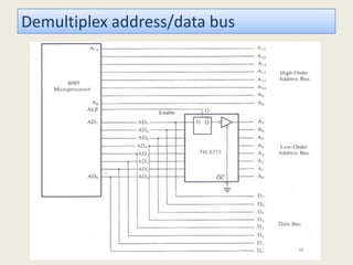
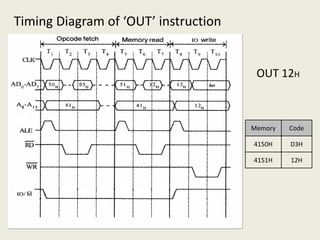
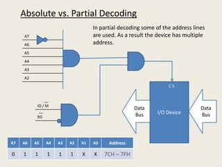
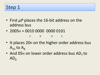
1. Pin diagram of 8085
2. I/O interfacing
INTEL 8085INTEL 8085 Pin ConfigurationPin Configuration
• The address bus has 8 signal lines A8 – A15 which are
unidirectional.
• The other 8 address bits are AD0 – AD7 multiplexed (time
shared) with the 8 data bits.
The Address and Data Bus Systems
– So, the bits AD0 – AD7 are bi-directional.
During the execution of the instruction, these
lines carry the address bits during the early
part, then during the late parts of the
execution, they carry the 8 data bits.
– In order to separate the address from the
data, we can use a latch to save the value
before the function of the bits changes.
Task
• Store a data 4FH (0100 1111) in the memory
location 2005H
FFFFH
microprocessor
2005H
0000H
Memory
4FH
Step 1
• First µP places the 16-bit address on the
address bus
• 2005H = 0010 0000 0000 0101
2 0 0 5
• It places 20H on the higher order address bus
A15 to A8
• And 05H on lower order address bus AD7 to
AD0
2 0 0 5
µP
0
0
1
0
0
0
0
0
0
A15
A8
AD
20H
µP 0
0
0
0
0
1
0
1
AD7
AD0
05H
Step 2
• Lower order address bus [AD7 to AD0] are connected with a latch
• Latch is such a device whose input = output
when it is activated
• ALE (Address Latch Enable) signal is
used to activate or deactivate the latch
when it is activated
• But when it is deactivated output does not
change with input
µP
0
0
1
0
0
0
0
0
0
A15
A8
AD
20H
µP 0
0
0
0
0
1
0
1
AD7
AD0
05H
Latch
ALE EN
0
0
0
0
0
1
0
1
Step 3
• Once the lower order address is latched µP
places the data on the data bus [AD7 to AD0]
• And generate an appropriate control signal to• And generate an appropriate control signal to
enable selected memory register
• Thus the data [4FH] is stored in memory
location 2005H
Demultiplex address/data bus
Control Signals for Read/Write Operations
• IO/M = > 1 data transfer between
microprocessor and peripherals (Input-
Output device)
• IO/M = > 0 data transfer between
microprocessor and memory
• RD=> Active low => Read operation
• WR=> Active low => Write operation
Status Signals
Timing Diagram for Memory Write
To write dataTo write data
4FH in the
memory
location 2005H
Timing Diagram for Memory Read
To read dataTo read data
from the
memory
location 2005H
I/O DEVICE
Devices other than memory are known as
I/O devices or Input-Output Devices
Interfacing of I/O device with 8085
In peripheral I/O, device is identified by an
8-bit address
In memory-mapped I/O, device is identified
by a 16-bit address
In 8-bit addressing mode
Maximum number of devices that can be
connected is 28 = 256
Address of the devices will be 00H, 01H, … … , FFHAddress of the devices will be 00H, 01H, … … , FFH
Both lower order 8 address bus (i.e. A0–A7) and
higher order 8 address bus (i.e. A8–A15) contains
the same 8-bit address
In 8-bit addressing mode
Only Accumulator is allowed for receiving or
transmitting data
Instruction to receive data from a device with
address C0H
Instruction to receive data from a device with
address C0H
IN C0H
Instruction to send data to a device with address
12H
OUT 12H
Timing Diagram of ‘IN’ instruction
IN C0H
Memory Code
4125H DBH
4126H C0H
Timing Diagram of ‘OUT’ instruction
OUT 12H
Memory Code
4150H D3H
4151H 12H
Device selection logic
A7
A6
A5
A4
A3
A2
A1
CS
Writing to an Output Port (7EH)
OUT 7EH
I/O Device
A1
A0
CS
Data
Bus
IO / M
WR
A7 A6 A5 A4 A3 A2 A1 A0 Address
0 1 1 1 1 1 1 0 7EH
Data
Bus
Device selection logic
A7
A6
A5
A4
A3
A2
A1
CS
Reading an Input Port (5DH)
IN 5DH
I/O Device
A1
A0
CS
IO / M
RD
A7 A6 A5 A4 A3 A2 A1 A0 Address
0 1 0 1 1 1 0 1 5DH
Data
Bus
Data
Bus
Absolute vs. Partial Decoding
A7
A6
A5
A4
A3
A2
CS
In partial decoding some of the address lines
are used. As a result the device has multiple
address.
I/O Device
CS
IO / M
RD
A7 A6 A5 A4 A3 A2 A1 A0 Address
0 1 1 1 1 1 X X 7CH – 7FH
Data
Bus
Data
Bus
A7 A6 A5 A4 A3 A2 A1 A0 Address
1 1 1 1 1 1 0 0 FC H
1 1 1 1 1 1 0 1 FD H
1 1 1 1 1 1 1 0 FE H
1 1 1 1 1 1 1 1 FF H
A7
A6
A5
Device 1
Device 2
Device 3
Device 4
Use of Decoder
2 to 4 Decoder
11
10
01
00
A0
A1
A4
A3
A2
CS
In memory-mapped addressing mode
I/O device will be treated as a memory register
Address of the devices will be 16-bitAddress of the devices will be 16-bit
Control signal IO/M pin should be low
All memory related instructions are allowed
Memory Mapped
I/O
16-bit device address
Data transfer between any general-
Peripheral Mapped
I/O
8-bit device address
Data is transfer only between accumulatorData transfer between any general-
purpose register and I/O port.
The memory map (64K) is shared between
I/O device and system memory.
More hardware is required to decode 16-
bit address
Arithmetic or logic operation can be
directly performed with I/O data
Data is transfer only between accumulator
and I.O port
Independent of the memory map; 256
input device and 256 output device can be
connected
Less hardware is required to decode 8-bit
address
-Arithmetic or logical operation cannot be
directly performed with I/O data

Microprocessor Part 2

  • 1.
    1. Pin diagramof 8085 2. I/O interfacing
  • 2.
    INTEL 8085INTEL 8085Pin ConfigurationPin Configuration
  • 3.
    • The addressbus has 8 signal lines A8 – A15 which are unidirectional. • The other 8 address bits are AD0 – AD7 multiplexed (time shared) with the 8 data bits. The Address and Data Bus Systems – So, the bits AD0 – AD7 are bi-directional. During the execution of the instruction, these lines carry the address bits during the early part, then during the late parts of the execution, they carry the 8 data bits. – In order to separate the address from the data, we can use a latch to save the value before the function of the bits changes.
  • 4.
    Task • Store adata 4FH (0100 1111) in the memory location 2005H FFFFH microprocessor 2005H 0000H Memory 4FH
  • 5.
    Step 1 • FirstµP places the 16-bit address on the address bus • 2005H = 0010 0000 0000 0101 2 0 0 5 • It places 20H on the higher order address bus A15 to A8 • And 05H on lower order address bus AD7 to AD0 2 0 0 5
  • 6.
  • 7.
    Step 2 • Lowerorder address bus [AD7 to AD0] are connected with a latch • Latch is such a device whose input = output when it is activated • ALE (Address Latch Enable) signal is used to activate or deactivate the latch when it is activated • But when it is deactivated output does not change with input
  • 8.
  • 9.
    Step 3 • Oncethe lower order address is latched µP places the data on the data bus [AD7 to AD0] • And generate an appropriate control signal to• And generate an appropriate control signal to enable selected memory register • Thus the data [4FH] is stored in memory location 2005H
  • 10.
  • 11.
    Control Signals forRead/Write Operations • IO/M = > 1 data transfer between microprocessor and peripherals (Input- Output device) • IO/M = > 0 data transfer between microprocessor and memory • RD=> Active low => Read operation • WR=> Active low => Write operation
  • 12.
  • 13.
    Timing Diagram forMemory Write To write dataTo write data 4FH in the memory location 2005H
  • 14.
    Timing Diagram forMemory Read To read dataTo read data from the memory location 2005H
  • 15.
  • 16.
    Devices other thanmemory are known as I/O devices or Input-Output Devices
  • 17.
    Interfacing of I/Odevice with 8085 In peripheral I/O, device is identified by an 8-bit address In memory-mapped I/O, device is identified by a 16-bit address
  • 18.
    In 8-bit addressingmode Maximum number of devices that can be connected is 28 = 256 Address of the devices will be 00H, 01H, … … , FFHAddress of the devices will be 00H, 01H, … … , FFH Both lower order 8 address bus (i.e. A0–A7) and higher order 8 address bus (i.e. A8–A15) contains the same 8-bit address
  • 19.
    In 8-bit addressingmode Only Accumulator is allowed for receiving or transmitting data Instruction to receive data from a device with address C0H Instruction to receive data from a device with address C0H IN C0H Instruction to send data to a device with address 12H OUT 12H
  • 20.
    Timing Diagram of‘IN’ instruction IN C0H Memory Code 4125H DBH 4126H C0H
  • 21.
    Timing Diagram of‘OUT’ instruction OUT 12H Memory Code 4150H D3H 4151H 12H
  • 22.
    Device selection logic A7 A6 A5 A4 A3 A2 A1 CS Writingto an Output Port (7EH) OUT 7EH I/O Device A1 A0 CS Data Bus IO / M WR A7 A6 A5 A4 A3 A2 A1 A0 Address 0 1 1 1 1 1 1 0 7EH Data Bus
  • 23.
    Device selection logic A7 A6 A5 A4 A3 A2 A1 CS Readingan Input Port (5DH) IN 5DH I/O Device A1 A0 CS IO / M RD A7 A6 A5 A4 A3 A2 A1 A0 Address 0 1 0 1 1 1 0 1 5DH Data Bus Data Bus
  • 24.
    Absolute vs. PartialDecoding A7 A6 A5 A4 A3 A2 CS In partial decoding some of the address lines are used. As a result the device has multiple address. I/O Device CS IO / M RD A7 A6 A5 A4 A3 A2 A1 A0 Address 0 1 1 1 1 1 X X 7CH – 7FH Data Bus Data Bus
  • 25.
    A7 A6 A5A4 A3 A2 A1 A0 Address 1 1 1 1 1 1 0 0 FC H 1 1 1 1 1 1 0 1 FD H 1 1 1 1 1 1 1 0 FE H 1 1 1 1 1 1 1 1 FF H A7 A6 A5 Device 1 Device 2 Device 3 Device 4 Use of Decoder 2 to 4 Decoder 11 10 01 00 A0 A1 A4 A3 A2 CS
  • 26.
    In memory-mapped addressingmode I/O device will be treated as a memory register Address of the devices will be 16-bitAddress of the devices will be 16-bit Control signal IO/M pin should be low All memory related instructions are allowed
  • 27.
    Memory Mapped I/O 16-bit deviceaddress Data transfer between any general- Peripheral Mapped I/O 8-bit device address Data is transfer only between accumulatorData transfer between any general- purpose register and I/O port. The memory map (64K) is shared between I/O device and system memory. More hardware is required to decode 16- bit address Arithmetic or logic operation can be directly performed with I/O data Data is transfer only between accumulator and I.O port Independent of the memory map; 256 input device and 256 output device can be connected Less hardware is required to decode 8-bit address -Arithmetic or logical operation cannot be directly performed with I/O data