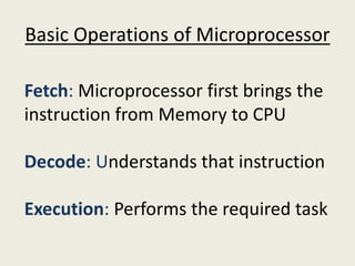
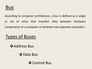
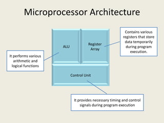
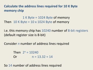
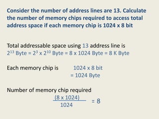
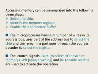
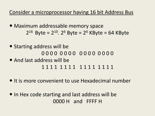
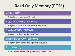
SlideShare a Scribd company logo
1 of 23
Download to read offline
1. General overview of microprocessor
2. Memory interfacing
What Microprocessor is ?
Multipurpose, Programmable, Clock driven
Electronics device or IC
Fetch: Microprocessor first brings the
instruction from Memory to CPU
Basic Operations of Microprocessor
Decode: Understands that instruction
Execution: Performs the required task
Basic parts of a μP Based System
• CPU (μP)
• Memory
• I/O devices
According to computer architecture, a bus is defined as a single
or set of wires that transfers data between hardware
components of a computer or between two separate computers.
Types of Buses
Bus
Types of Buses
Address Bus
Data Bus
Control Bus
Control Bus
 Generally contains one wire
 Generates control signals
 Some control signals are Read, Write and
Opcode fetch etc.
Data Bus
A set of bidirectional wires
Sends or receives data or information
Number of wires used in a data bus is known as its
widthwidth
A microprocessor is generally known with its data bus
width
There are two types of data transfer; Serial data
transfer and Parallel data transfer
Address Bus
 A set of unidirectional wires are used to
select a device
 With nn – digit numbering system we can With nn – digit numbering system we can
addressed maximum 22nn number of houses
 Microprocessor having 16 bit address bus
can communicate with 221616 or 65,53665,536
numbers of devices
Microprocessor Architecture
ALU
Register
Array
Contains various
registers that store
data temporarily
during program
execution.
It performs various
arithmetic and
Control Unit
It provides necessary timing and control
signals during program execution
arithmetic and
logical functions
First Generation
Between 1971 – 1973
PMOS technology, non compatible with TTL
4 bit processors  16 pins
8 and 16 bit processors  40 pins
Due to limitations of pins, signals are
multiplexed
Second Generation
During 1973
NMOS technology  Faster speed, Higher
density, Compatible with TTL
4 / 8/ 16 bit processors  40 pins
Ability to address large memory spaces
and I/O ports
Greater number of levels of subroutine
nesting
Better interrupt handling capabilities
Intel 8085 (8 bit processor)
Third Generation
During 1978
HMOS technology  Faster speed, Higher
packing density
16 bit processors  40/ 48/ 64 pins
Historical Background
16 bit processors  40/ 48/ 64 pins
Easier to program
Dynamically relatable programs
Processor has multiply/ divide arithmetic
hardware
More powerful interrupt handling
capabilities
Flexible I/O port addressing
Intel 8086 (16 bit processor)
Fourth Generation
During 1980s
Low power version of HMOS technology
(HCMOS)
32 bit processors
Physical memory space 224 bytes = 16 Mb
Virtual memory space 240 bytes = 1 Tb
Floating point hardware
Supports increased number of addressing
modes
Intel 80386
Fifth Generation Pentium
MEMORY
A single Flip-Flop / Capacitor can store one
bit – 0 or 1
8 Flip-Flops together will form an 8-bit
RegisterRegister
An 8-bit register can stores 8-bit or 1 Byte
data
A set of 8-bit register will form a
Memory
Ten 8-bit registers
i.e. 10 bytes of
memorymemory
can store 10 bytes
of data
10 x 8 bit memory
Or
10 byte memory
11 Register 3
10 Register 2
01 Register 1
00 Register 0
Accessing Memory or Memory Interfacing
2 to 4 Decoder
00
01
10
11
A0
A1
Calculate the address lines required for 10 K Byte
memory chip
1 K Byte = 1024 Byte of memory
Then 10 K Byte = 10 x 1024 Byte of memory
i.e. this memory chip has 10240 number of 8-bit registers
(default register size is 8-bit)(default register size is 8-bit)
Consider n number of address lines required
Then 2n = 10240
Or n = 13.32 ≈ 14
So 14 number of address lines required
Consider the number of address lines are 13. Calculate
the number of memory chips required to access total
address space if each memory chip is 1024 x 8 bit
Total addressable space using 13 address line is
213 Byte = 23 x 210 Byte = 8 x 1024 Byte = 8 K Byte
Each memory chip is 1024 x 8 bit
= 1024 Byte
Number of memory chip required
(8 x 1024)
1024
= 8
Accessing memory can be summarized into the following
three steps:
 Select the chip.
 Identify the memory register.
 Enable the appropriate buffer.
The microprocessor having N number of wires in its
address bus; uses part of the address bus to select the
The microprocessor having N number of wires in its
address bus; uses part of the address bus to select the
chip and the remaining part goes through the address
decoder to select the register.
The control signals IO/M (to select I/O device or
memory), WR (enable writing) and RD (enable reading)
are used to activate the operation.
Consider a microprocessor having 16 bit Address Bus
 Maximum addressable memory space
216 Byte = 210. 26 Byte = 26 KByte = 64 KByte
 Starting address will be
0 0 0 0 0 0 0 0 0 0 0 0 0 0 0 0
 And last address will be And last address will be
1 1 1 1 1 1 1 1 1 1 1 1 1 1 1 1
 It is more convenient to use Hexadecimal number
 In Hex code starting and last address will be
0000 H and FFFF H
Explain the memory address range
A15 A14 A13 A12 A11 A10 A9 A8 A7 A6 A5 A4 A3 A2 A1 A0 Address
0 0 0 0 0 0 0 0 0 0 0 0 0 0 0 0 0000H
0 0 0 0 1 1 1 1 1 1 1 1 1 1 1 1 0FFFH
A15
A14
A13
A12
A11
A10
A9
Draw the memory map to access 256 Byte
memory using 16 bit address line
256 Byte
A7
A6
A5
CS
A9
A8
A15 A14 A13 A12 A11 A10 A9 A8 A7 A6 A5 A4 A3 A2 A1 A0 Address
0 1 1 1 1 1 1 1 0 0 0 0 0 0 0 0 7F00H
0 1 1 1 1 1 1 1 1 1 1 1 1 1 1 1 7FFFH
256 Byte
Memory
A4
A3
A2
A1
A0
For addressing 256 Byte memory we
required only 8 address line (A0 to A7).
Remaining 8 address lines (A8 to A15) is
used of chip selection
Memory
Primary
Memory
RAM ROM
Secondary
Memory
Hard Disk,
Memory
Classification
RAM
Static RAM
Dynamic
RAM
ROM
Erasable
EPROM EEPROM
Flash
Memory
Permanent
Masked
ROM
PROM
Hard Disk,
Floppy, CD
Random Access Memory (RAM)
• Stores bit as voltage
• High speed
• More expensive
• High power consumption
Static RAM (SRAM)
• High power consumption
• Stores bit as charge
• Low speed
• Less expensive
• Low power consumption
• Requires frequent refreshing
Dynamic RAM (DRAM)
Read Only Memory (ROM)
Masked ROM
• Bit pattern is permanently masked
Programmable ROM (PROM)
• Program is burnt into the memory only once
Erasable PROM (EPROM)
• Program can be erased using UV ray
Electrically EPROM (EEPROM)
• Program can be erased using electrical signals
Flash Memory
• It can be erased and reprogrammed a million times

More Related Content

What's hot

Introduction of 8086 micro processor .
Introduction of 8086 micro processor .Introduction of 8086 micro processor .
Introduction of 8086 micro processor .Siraj Ahmed
 
MAI-introduction of memory and i/o device with 8085
MAI-introduction of memory and i/o device with 8085MAI-introduction of memory and i/o device with 8085
MAI-introduction of memory and i/o device with 8085Ðîgëñ Tàìlør
 
Microprocessor 8085 Chapter 4
Microprocessor 8085 Chapter 4Microprocessor 8085 Chapter 4
Microprocessor 8085 Chapter 4Rishikesh Bhavsar
 
Architecture OF 8085
Architecture OF 8085Architecture OF 8085
Architecture OF 8085muneer.k
 
Memory intrface and addrs modes
Memory intrface and addrs modesMemory intrface and addrs modes
Memory intrface and addrs modesbalbirvirdi
 
Interfacing of io device to 8085
Interfacing of io device to 8085Interfacing of io device to 8085
Interfacing of io device to 8085Nitin Ahire
 
8085 Interfacing with I/O Devices or Memory
8085 Interfacing with I/O Devices or Memory8085 Interfacing with I/O Devices or Memory
8085 Interfacing with I/O Devices or MemorySaumay Paul
 
Detailed Explanation of Pin Description of 8085 microprocessor
Detailed Explanation of Pin Description of  8085 microprocessorDetailed Explanation of Pin Description of  8085 microprocessor
Detailed Explanation of Pin Description of 8085 microprocessorRamesh Dabhole
 
Microprocessor 8086
Microprocessor 8086Microprocessor 8086
Microprocessor 8086Umang Dhuri
 
PIN Specification of 8086 Microprocessor
PIN Specification of 8086 MicroprocessorPIN Specification of 8086 Microprocessor
PIN Specification of 8086 MicroprocessorNikhil Kumar
 
8085 Architecture
8085 Architecture8085 Architecture
8085 Architecturedeval patel
 
Pin configuration of 8085
Pin configuration of 8085Pin configuration of 8085
Pin configuration of 808582338476
 

What's hot (20)

Chapter 5
Chapter 5Chapter 5
Chapter 5
 
Introduction of 8086 micro processor .
Introduction of 8086 micro processor .Introduction of 8086 micro processor .
Introduction of 8086 micro processor .
 
MAI-introduction of memory and i/o device with 8085
MAI-introduction of memory and i/o device with 8085MAI-introduction of memory and i/o device with 8085
MAI-introduction of memory and i/o device with 8085
 
Microprocessor 8085 Chapter 4
Microprocessor 8085 Chapter 4Microprocessor 8085 Chapter 4
Microprocessor 8085 Chapter 4
 
8086 Microprocessor
8086 Microprocessor8086 Microprocessor
8086 Microprocessor
 
Architecture OF 8085
Architecture OF 8085Architecture OF 8085
Architecture OF 8085
 
Memory intrface and addrs modes
Memory intrface and addrs modesMemory intrface and addrs modes
Memory intrface and addrs modes
 
8086 architecture
8086 architecture8086 architecture
8086 architecture
 
Interfacing of io device to 8085
Interfacing of io device to 8085Interfacing of io device to 8085
Interfacing of io device to 8085
 
8086 new
8086 new8086 new
8086 new
 
8085 Interfacing with I/O Devices or Memory
8085 Interfacing with I/O Devices or Memory8085 Interfacing with I/O Devices or Memory
8085 Interfacing with I/O Devices or Memory
 
8086 MICROPROCESSOR
8086 MICROPROCESSOR8086 MICROPROCESSOR
8086 MICROPROCESSOR
 
8086 ppt
8086 ppt8086 ppt
8086 ppt
 
Detailed Explanation of Pin Description of 8085 microprocessor
Detailed Explanation of Pin Description of  8085 microprocessorDetailed Explanation of Pin Description of  8085 microprocessor
Detailed Explanation of Pin Description of 8085 microprocessor
 
Chapter5
Chapter5Chapter5
Chapter5
 
Lecture2
Lecture2Lecture2
Lecture2
 
Microprocessor 8086
Microprocessor 8086Microprocessor 8086
Microprocessor 8086
 
PIN Specification of 8086 Microprocessor
PIN Specification of 8086 MicroprocessorPIN Specification of 8086 Microprocessor
PIN Specification of 8086 Microprocessor
 
8085 Architecture
8085 Architecture8085 Architecture
8085 Architecture
 
Pin configuration of 8085
Pin configuration of 8085Pin configuration of 8085
Pin configuration of 8085
 

Similar to Microprocessor Part 1

Micro[processor
Micro[processorMicro[processor
Micro[processorcollege
 
Microprocessor 8086 nitin_p
Microprocessor 8086 nitin_pMicroprocessor 8086 nitin_p
Microprocessor 8086 nitin_pnitinahire15
 
Microprocessor 8086 8087_nitin ahire
Microprocessor 8086 8087_nitin ahireMicroprocessor 8086 8087_nitin ahire
Microprocessor 8086 8087_nitin ahireNitin Ahire
 
8086 architecture-unit-1
8086 architecture-unit-18086 architecture-unit-1
8086 architecture-unit-1logesh.ieee
 
8086 architecture and pin description
8086 architecture and pin description 8086 architecture and pin description
8086 architecture and pin description Aswini Dharmaraj
 
Students corner131
Students corner131Students corner131
Students corner131Satti286
 
Interfacing memory with 8086 microprocessor
Interfacing memory with 8086 microprocessorInterfacing memory with 8086 microprocessor
Interfacing memory with 8086 microprocessorVikas Gupta
 
memeoryorganization PPT for organization of memories
memeoryorganization PPT for organization of memoriesmemeoryorganization PPT for organization of memories
memeoryorganization PPT for organization of memoriesGauravDaware2
 
Chp3 designing bus system, memory & io copy
Chp3 designing bus system, memory & io   copyChp3 designing bus system, memory & io   copy
Chp3 designing bus system, memory & io copymkazree
 
EC 8691 Microprocessor and Microcontroller.pptx
EC 8691 Microprocessor and Microcontroller.pptxEC 8691 Microprocessor and Microcontroller.pptx
EC 8691 Microprocessor and Microcontroller.pptxGobinathAECEJRF1101
 
8086_architecture MMC PPT.ppt
8086_architecture MMC PPT.ppt8086_architecture MMC PPT.ppt
8086_architecture MMC PPT.pptJamesAlpha3
 
8086 slide general short notes assembly languages.pptx
8086 slide general short notes assembly languages.pptx8086 slide general short notes assembly languages.pptx
8086 slide general short notes assembly languages.pptxbinaboss24
 
UNIT-II-8086.pptx
UNIT-II-8086.pptxUNIT-II-8086.pptx
UNIT-II-8086.pptxparul757596
 
Session01_Intro.pdf
Session01_Intro.pdfSession01_Intro.pdf
Session01_Intro.pdfRahnerJames
 
Notes-7_complete notes_8086.pdf
Notes-7_complete notes_8086.pdfNotes-7_complete notes_8086.pdf
Notes-7_complete notes_8086.pdfVisheshYadav38
 
Intel 8086 microprocessor
Intel 8086 microprocessorIntel 8086 microprocessor
Intel 8086 microprocessorRavi Yasas
 

Similar to Microprocessor Part 1 (20)

Micro[processor
Micro[processorMicro[processor
Micro[processor
 
Register & Memory
Register & MemoryRegister & Memory
Register & Memory
 
Microprocessor 8086 nitin_p
Microprocessor 8086 nitin_pMicroprocessor 8086 nitin_p
Microprocessor 8086 nitin_p
 
Microprocessor 8086 8087_nitin ahire
Microprocessor 8086 8087_nitin ahireMicroprocessor 8086 8087_nitin ahire
Microprocessor 8086 8087_nitin ahire
 
8086 architecture-unit-1
8086 architecture-unit-18086 architecture-unit-1
8086 architecture-unit-1
 
8086 architecture and pin description
8086 architecture and pin description 8086 architecture and pin description
8086 architecture and pin description
 
Students corner131
Students corner131Students corner131
Students corner131
 
Interfacing memory with 8086 microprocessor
Interfacing memory with 8086 microprocessorInterfacing memory with 8086 microprocessor
Interfacing memory with 8086 microprocessor
 
memeoryorganization PPT for organization of memories
memeoryorganization PPT for organization of memoriesmemeoryorganization PPT for organization of memories
memeoryorganization PPT for organization of memories
 
Chp3 designing bus system, memory & io copy
Chp3 designing bus system, memory & io   copyChp3 designing bus system, memory & io   copy
Chp3 designing bus system, memory & io copy
 
EC 8691 Microprocessor and Microcontroller.pptx
EC 8691 Microprocessor and Microcontroller.pptxEC 8691 Microprocessor and Microcontroller.pptx
EC 8691 Microprocessor and Microcontroller.pptx
 
8086slide
8086slide8086slide
8086slide
 
8086_architecture MMC PPT.ppt
8086_architecture MMC PPT.ppt8086_architecture MMC PPT.ppt
8086_architecture MMC PPT.ppt
 
8086 slide general short notes assembly languages.pptx
8086 slide general short notes assembly languages.pptx8086 slide general short notes assembly languages.pptx
8086 slide general short notes assembly languages.pptx
 
UNIT-II-8086.pptx
UNIT-II-8086.pptxUNIT-II-8086.pptx
UNIT-II-8086.pptx
 
Session01_Intro.pdf
Session01_Intro.pdfSession01_Intro.pdf
Session01_Intro.pdf
 
8086 mprocessor.pptx
8086 mprocessor.pptx8086 mprocessor.pptx
8086 mprocessor.pptx
 
Notes-7_complete notes_8086.pdf
Notes-7_complete notes_8086.pdfNotes-7_complete notes_8086.pdf
Notes-7_complete notes_8086.pdf
 
Intel 8086 microprocessor
Intel 8086 microprocessorIntel 8086 microprocessor
Intel 8086 microprocessor
 
Chapter 9
Chapter 9Chapter 9
Chapter 9
 

Recently uploaded

Software and Systems Engineering Standards: Verification and Validation of Sy...
Software and Systems Engineering Standards: Verification and Validation of Sy...Software and Systems Engineering Standards: Verification and Validation of Sy...
Software and Systems Engineering Standards: Verification and Validation of Sy...VICTOR MAESTRE RAMIREZ
 
Artificial-Intelligence-in-Electronics (K).pptx
Artificial-Intelligence-in-Electronics (K).pptxArtificial-Intelligence-in-Electronics (K).pptx
Artificial-Intelligence-in-Electronics (K).pptxbritheesh05
 
power system scada applications and uses
power system scada applications and usespower system scada applications and uses
power system scada applications and usesDevarapalliHaritha
 
CCS355 Neural Network & Deep Learning UNIT III notes and Question bank .pdf
CCS355 Neural Network & Deep Learning UNIT III notes and Question bank .pdfCCS355 Neural Network & Deep Learning UNIT III notes and Question bank .pdf
CCS355 Neural Network & Deep Learning UNIT III notes and Question bank .pdfAsst.prof M.Gokilavani
 
HARMONY IN THE HUMAN BEING - Unit-II UHV-2
HARMONY IN THE HUMAN BEING - Unit-II UHV-2HARMONY IN THE HUMAN BEING - Unit-II UHV-2
HARMONY IN THE HUMAN BEING - Unit-II UHV-2RajaP95
 
GDSC ASEB Gen AI study jams presentation
GDSC ASEB Gen AI study jams presentationGDSC ASEB Gen AI study jams presentation
GDSC ASEB Gen AI study jams presentationGDSCAESB
 
Current Transformer Drawing and GTP for MSETCL
Current Transformer Drawing and GTP for MSETCLCurrent Transformer Drawing and GTP for MSETCL
Current Transformer Drawing and GTP for MSETCLDeelipZope
 
APPLICATIONS-AC/DC DRIVES-OPERATING CHARACTERISTICS
APPLICATIONS-AC/DC DRIVES-OPERATING CHARACTERISTICSAPPLICATIONS-AC/DC DRIVES-OPERATING CHARACTERISTICS
APPLICATIONS-AC/DC DRIVES-OPERATING CHARACTERISTICSKurinjimalarL3
 
CCS355 Neural Network & Deep Learning Unit II Notes with Question bank .pdf
CCS355 Neural Network & Deep Learning Unit II Notes with Question bank .pdfCCS355 Neural Network & Deep Learning Unit II Notes with Question bank .pdf
CCS355 Neural Network & Deep Learning Unit II Notes with Question bank .pdfAsst.prof M.Gokilavani
 
Gurgaon ✡️9711147426✨Call In girls Gurgaon Sector 51 escort service
Gurgaon ✡️9711147426✨Call In girls Gurgaon Sector 51 escort serviceGurgaon ✡️9711147426✨Call In girls Gurgaon Sector 51 escort service
Gurgaon ✡️9711147426✨Call In girls Gurgaon Sector 51 escort servicejennyeacort
 
chaitra-1.pptx fake news detection using machine learning
chaitra-1.pptx  fake news detection using machine learningchaitra-1.pptx  fake news detection using machine learning
chaitra-1.pptx fake news detection using machine learningmisbanausheenparvam
 
Decoding Kotlin - Your guide to solving the mysterious in Kotlin.pptx
Decoding Kotlin - Your guide to solving the mysterious in Kotlin.pptxDecoding Kotlin - Your guide to solving the mysterious in Kotlin.pptx
Decoding Kotlin - Your guide to solving the mysterious in Kotlin.pptxJoão Esperancinha
 
SPICE PARK APR2024 ( 6,793 SPICE Models )
SPICE PARK APR2024 ( 6,793 SPICE Models )SPICE PARK APR2024 ( 6,793 SPICE Models )
SPICE PARK APR2024 ( 6,793 SPICE Models )Tsuyoshi Horigome
 
College Call Girls Nashik Nehal 7001305949 Independent Escort Service Nashik
College Call Girls Nashik Nehal 7001305949 Independent Escort Service NashikCollege Call Girls Nashik Nehal 7001305949 Independent Escort Service Nashik
College Call Girls Nashik Nehal 7001305949 Independent Escort Service NashikCall Girls in Nagpur High Profile
 
HARMONY IN THE NATURE AND EXISTENCE - Unit-IV
HARMONY IN THE NATURE AND EXISTENCE - Unit-IVHARMONY IN THE NATURE AND EXISTENCE - Unit-IV
HARMONY IN THE NATURE AND EXISTENCE - Unit-IVRajaP95
 
Sachpazis Costas: Geotechnical Engineering: A student's Perspective Introduction
Sachpazis Costas: Geotechnical Engineering: A student's Perspective IntroductionSachpazis Costas: Geotechnical Engineering: A student's Perspective Introduction
Sachpazis Costas: Geotechnical Engineering: A student's Perspective IntroductionDr.Costas Sachpazis
 
Sheet Pile Wall Design and Construction: A Practical Guide for Civil Engineer...
Sheet Pile Wall Design and Construction: A Practical Guide for Civil Engineer...Sheet Pile Wall Design and Construction: A Practical Guide for Civil Engineer...
Sheet Pile Wall Design and Construction: A Practical Guide for Civil Engineer...Dr.Costas Sachpazis
 
main PPT.pptx of girls hostel security using rfid
main PPT.pptx of girls hostel security using rfidmain PPT.pptx of girls hostel security using rfid
main PPT.pptx of girls hostel security using rfidNikhilNagaraju
 

Recently uploaded (20)

Software and Systems Engineering Standards: Verification and Validation of Sy...
Software and Systems Engineering Standards: Verification and Validation of Sy...Software and Systems Engineering Standards: Verification and Validation of Sy...
Software and Systems Engineering Standards: Verification and Validation of Sy...
 
Artificial-Intelligence-in-Electronics (K).pptx
Artificial-Intelligence-in-Electronics (K).pptxArtificial-Intelligence-in-Electronics (K).pptx
Artificial-Intelligence-in-Electronics (K).pptx
 
power system scada applications and uses
power system scada applications and usespower system scada applications and uses
power system scada applications and uses
 
9953056974 Call Girls In South Ex, Escorts (Delhi) NCR.pdf
9953056974 Call Girls In South Ex, Escorts (Delhi) NCR.pdf9953056974 Call Girls In South Ex, Escorts (Delhi) NCR.pdf
9953056974 Call Girls In South Ex, Escorts (Delhi) NCR.pdf
 
CCS355 Neural Network & Deep Learning UNIT III notes and Question bank .pdf
CCS355 Neural Network & Deep Learning UNIT III notes and Question bank .pdfCCS355 Neural Network & Deep Learning UNIT III notes and Question bank .pdf
CCS355 Neural Network & Deep Learning UNIT III notes and Question bank .pdf
 
HARMONY IN THE HUMAN BEING - Unit-II UHV-2
HARMONY IN THE HUMAN BEING - Unit-II UHV-2HARMONY IN THE HUMAN BEING - Unit-II UHV-2
HARMONY IN THE HUMAN BEING - Unit-II UHV-2
 
🔝9953056974🔝!!-YOUNG call girls in Rajendra Nagar Escort rvice Shot 2000 nigh...
🔝9953056974🔝!!-YOUNG call girls in Rajendra Nagar Escort rvice Shot 2000 nigh...🔝9953056974🔝!!-YOUNG call girls in Rajendra Nagar Escort rvice Shot 2000 nigh...
🔝9953056974🔝!!-YOUNG call girls in Rajendra Nagar Escort rvice Shot 2000 nigh...
 
GDSC ASEB Gen AI study jams presentation
GDSC ASEB Gen AI study jams presentationGDSC ASEB Gen AI study jams presentation
GDSC ASEB Gen AI study jams presentation
 
Current Transformer Drawing and GTP for MSETCL
Current Transformer Drawing and GTP for MSETCLCurrent Transformer Drawing and GTP for MSETCL
Current Transformer Drawing and GTP for MSETCL
 
APPLICATIONS-AC/DC DRIVES-OPERATING CHARACTERISTICS
APPLICATIONS-AC/DC DRIVES-OPERATING CHARACTERISTICSAPPLICATIONS-AC/DC DRIVES-OPERATING CHARACTERISTICS
APPLICATIONS-AC/DC DRIVES-OPERATING CHARACTERISTICS
 
CCS355 Neural Network & Deep Learning Unit II Notes with Question bank .pdf
CCS355 Neural Network & Deep Learning Unit II Notes with Question bank .pdfCCS355 Neural Network & Deep Learning Unit II Notes with Question bank .pdf
CCS355 Neural Network & Deep Learning Unit II Notes with Question bank .pdf
 
Gurgaon ✡️9711147426✨Call In girls Gurgaon Sector 51 escort service
Gurgaon ✡️9711147426✨Call In girls Gurgaon Sector 51 escort serviceGurgaon ✡️9711147426✨Call In girls Gurgaon Sector 51 escort service
Gurgaon ✡️9711147426✨Call In girls Gurgaon Sector 51 escort service
 
chaitra-1.pptx fake news detection using machine learning
chaitra-1.pptx  fake news detection using machine learningchaitra-1.pptx  fake news detection using machine learning
chaitra-1.pptx fake news detection using machine learning
 
Decoding Kotlin - Your guide to solving the mysterious in Kotlin.pptx
Decoding Kotlin - Your guide to solving the mysterious in Kotlin.pptxDecoding Kotlin - Your guide to solving the mysterious in Kotlin.pptx
Decoding Kotlin - Your guide to solving the mysterious in Kotlin.pptx
 
SPICE PARK APR2024 ( 6,793 SPICE Models )
SPICE PARK APR2024 ( 6,793 SPICE Models )SPICE PARK APR2024 ( 6,793 SPICE Models )
SPICE PARK APR2024 ( 6,793 SPICE Models )
 
College Call Girls Nashik Nehal 7001305949 Independent Escort Service Nashik
College Call Girls Nashik Nehal 7001305949 Independent Escort Service NashikCollege Call Girls Nashik Nehal 7001305949 Independent Escort Service Nashik
College Call Girls Nashik Nehal 7001305949 Independent Escort Service Nashik
 
HARMONY IN THE NATURE AND EXISTENCE - Unit-IV
HARMONY IN THE NATURE AND EXISTENCE - Unit-IVHARMONY IN THE NATURE AND EXISTENCE - Unit-IV
HARMONY IN THE NATURE AND EXISTENCE - Unit-IV
 
Sachpazis Costas: Geotechnical Engineering: A student's Perspective Introduction
Sachpazis Costas: Geotechnical Engineering: A student's Perspective IntroductionSachpazis Costas: Geotechnical Engineering: A student's Perspective Introduction
Sachpazis Costas: Geotechnical Engineering: A student's Perspective Introduction
 
Sheet Pile Wall Design and Construction: A Practical Guide for Civil Engineer...
Sheet Pile Wall Design and Construction: A Practical Guide for Civil Engineer...Sheet Pile Wall Design and Construction: A Practical Guide for Civil Engineer...
Sheet Pile Wall Design and Construction: A Practical Guide for Civil Engineer...
 
main PPT.pptx of girls hostel security using rfid
main PPT.pptx of girls hostel security using rfidmain PPT.pptx of girls hostel security using rfid
main PPT.pptx of girls hostel security using rfid
 

Microprocessor Part 1

  • 1. 1. General overview of microprocessor 2. Memory interfacing
  • 2. What Microprocessor is ? Multipurpose, Programmable, Clock driven Electronics device or IC
  • 3. Fetch: Microprocessor first brings the instruction from Memory to CPU Basic Operations of Microprocessor Decode: Understands that instruction Execution: Performs the required task
  • 4. Basic parts of a μP Based System • CPU (μP) • Memory • I/O devices
  • 5. According to computer architecture, a bus is defined as a single or set of wires that transfers data between hardware components of a computer or between two separate computers. Types of Buses Bus Types of Buses Address Bus Data Bus Control Bus
  • 6. Control Bus  Generally contains one wire  Generates control signals  Some control signals are Read, Write and Opcode fetch etc.
  • 7. Data Bus A set of bidirectional wires Sends or receives data or information Number of wires used in a data bus is known as its widthwidth A microprocessor is generally known with its data bus width There are two types of data transfer; Serial data transfer and Parallel data transfer
  • 8. Address Bus  A set of unidirectional wires are used to select a device  With nn – digit numbering system we can With nn – digit numbering system we can addressed maximum 22nn number of houses  Microprocessor having 16 bit address bus can communicate with 221616 or 65,53665,536 numbers of devices
  • 9. Microprocessor Architecture ALU Register Array Contains various registers that store data temporarily during program execution. It performs various arithmetic and Control Unit It provides necessary timing and control signals during program execution arithmetic and logical functions
  • 10. First Generation Between 1971 – 1973 PMOS technology, non compatible with TTL 4 bit processors  16 pins 8 and 16 bit processors  40 pins Due to limitations of pins, signals are multiplexed Second Generation During 1973 NMOS technology  Faster speed, Higher density, Compatible with TTL 4 / 8/ 16 bit processors  40 pins Ability to address large memory spaces and I/O ports Greater number of levels of subroutine nesting Better interrupt handling capabilities Intel 8085 (8 bit processor) Third Generation During 1978 HMOS technology  Faster speed, Higher packing density 16 bit processors  40/ 48/ 64 pins Historical Background 16 bit processors  40/ 48/ 64 pins Easier to program Dynamically relatable programs Processor has multiply/ divide arithmetic hardware More powerful interrupt handling capabilities Flexible I/O port addressing Intel 8086 (16 bit processor) Fourth Generation During 1980s Low power version of HMOS technology (HCMOS) 32 bit processors Physical memory space 224 bytes = 16 Mb Virtual memory space 240 bytes = 1 Tb Floating point hardware Supports increased number of addressing modes Intel 80386 Fifth Generation Pentium
  • 12. A single Flip-Flop / Capacitor can store one bit – 0 or 1 8 Flip-Flops together will form an 8-bit RegisterRegister An 8-bit register can stores 8-bit or 1 Byte data
  • 13. A set of 8-bit register will form a Memory Ten 8-bit registers i.e. 10 bytes of memorymemory can store 10 bytes of data 10 x 8 bit memory Or 10 byte memory
  • 14. 11 Register 3 10 Register 2 01 Register 1 00 Register 0 Accessing Memory or Memory Interfacing 2 to 4 Decoder 00 01 10 11 A0 A1
  • 15. Calculate the address lines required for 10 K Byte memory chip 1 K Byte = 1024 Byte of memory Then 10 K Byte = 10 x 1024 Byte of memory i.e. this memory chip has 10240 number of 8-bit registers (default register size is 8-bit)(default register size is 8-bit) Consider n number of address lines required Then 2n = 10240 Or n = 13.32 ≈ 14 So 14 number of address lines required
  • 16. Consider the number of address lines are 13. Calculate the number of memory chips required to access total address space if each memory chip is 1024 x 8 bit Total addressable space using 13 address line is 213 Byte = 23 x 210 Byte = 8 x 1024 Byte = 8 K Byte Each memory chip is 1024 x 8 bit = 1024 Byte Number of memory chip required (8 x 1024) 1024 = 8
  • 17. Accessing memory can be summarized into the following three steps:  Select the chip.  Identify the memory register.  Enable the appropriate buffer. The microprocessor having N number of wires in its address bus; uses part of the address bus to select the The microprocessor having N number of wires in its address bus; uses part of the address bus to select the chip and the remaining part goes through the address decoder to select the register. The control signals IO/M (to select I/O device or memory), WR (enable writing) and RD (enable reading) are used to activate the operation.
  • 18. Consider a microprocessor having 16 bit Address Bus  Maximum addressable memory space 216 Byte = 210. 26 Byte = 26 KByte = 64 KByte  Starting address will be 0 0 0 0 0 0 0 0 0 0 0 0 0 0 0 0  And last address will be And last address will be 1 1 1 1 1 1 1 1 1 1 1 1 1 1 1 1  It is more convenient to use Hexadecimal number  In Hex code starting and last address will be 0000 H and FFFF H
  • 19. Explain the memory address range A15 A14 A13 A12 A11 A10 A9 A8 A7 A6 A5 A4 A3 A2 A1 A0 Address 0 0 0 0 0 0 0 0 0 0 0 0 0 0 0 0 0000H 0 0 0 0 1 1 1 1 1 1 1 1 1 1 1 1 0FFFH
  • 20. A15 A14 A13 A12 A11 A10 A9 Draw the memory map to access 256 Byte memory using 16 bit address line 256 Byte A7 A6 A5 CS A9 A8 A15 A14 A13 A12 A11 A10 A9 A8 A7 A6 A5 A4 A3 A2 A1 A0 Address 0 1 1 1 1 1 1 1 0 0 0 0 0 0 0 0 7F00H 0 1 1 1 1 1 1 1 1 1 1 1 1 1 1 1 7FFFH 256 Byte Memory A4 A3 A2 A1 A0 For addressing 256 Byte memory we required only 8 address line (A0 to A7). Remaining 8 address lines (A8 to A15) is used of chip selection
  • 21. Memory Primary Memory RAM ROM Secondary Memory Hard Disk, Memory Classification RAM Static RAM Dynamic RAM ROM Erasable EPROM EEPROM Flash Memory Permanent Masked ROM PROM Hard Disk, Floppy, CD
  • 22. Random Access Memory (RAM) • Stores bit as voltage • High speed • More expensive • High power consumption Static RAM (SRAM) • High power consumption • Stores bit as charge • Low speed • Less expensive • Low power consumption • Requires frequent refreshing Dynamic RAM (DRAM)
  • 23. Read Only Memory (ROM) Masked ROM • Bit pattern is permanently masked Programmable ROM (PROM) • Program is burnt into the memory only once Erasable PROM (EPROM) • Program can be erased using UV ray Electrically EPROM (EEPROM) • Program can be erased using electrical signals Flash Memory • It can be erased and reprogrammed a million times