SlideShare a Scribd company logo
8085 interfacing with memory Chips
*
Microprocessor need to access memory quite frequently to read
instructions and data stored in memory; the interface circuit enables that
access.
The interface process involves designing a circuit that will match the memory
requirements with the microprocessor signal.[Memory has certain signal
requirements to read from and write into memory. Similarly
Microprocessor initiates the set of signals when it wants to read from
and write into memory].
Memory Structure and its Requirements
*
R/W Memory: Group of Registers.
Figure Shows:
●2048 registers
●Register store 8-bits
●8 input, 8-output lines
●11 address lines(AD10-AD0), 1 chip
select, 2 control lines to enable input
and output buffer.
●Internal decoder to decode address
lines
Fig: R/W Static Memory
Memory Structure and its Requirements
*
EPROM : Chip must be programmed
before it can be used as ROM.
●4096 (4K) registers.
●Register store 8-bits
●8 input lines
●Internal decoder to decode address
lines.
●12 address lines(A11-A0),
● 1 chip select
● 1 Read control Signal lines to
enable output buffer.
Fig: EPROM
Basic concepts of Memory Interfacing
*
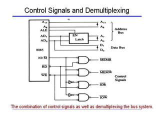
● 8085 places 16-bit address on address bus
● 11 low order address lines are required to
select the register for EPROM.
●Remaining 8085 address lines (A15-A11)
should be decoded to generate chip select.
●MEMR’. MEMW’ control signals that can be
used to enable buffer for read and write
operations.
●Memory places data byte from address
register during T2 and that is read by the
microprocessor before the end of T3.
Fig: Timing Diagram of Memory Write Cycle
Basic concepts of Memory Interfacing
*
Primary Function of memory
interfacing is that the microprocessor
should be able to read from and write
into a given register of a memory chip:
●Select the Chip
●Identify the register
●Enable the appropriate buffer.
Timing Diagram of 8085 Memory
Read/Write Machine Cycle allows to
understand microprocessor
interfacing concepts.
Fig: Timing Diagram of Memory Read
Cycle
Basic concepts of Memory Interfacing
*
Address Decoding and Memory Addresses
*
●EPROM Address Lines A11-A0 are connected to memory
chip.
●Remaining Address lines A15-A12 of 8085
microprocessor must be decoded.
●Two methods to decoding these lines:
●by NAND gate: Output of NAND gate is active and select
the chip only when all address lines A15-A12 are at logic1
●by using 3x8 Decoder: If enable line is active eight
different logic combination can be identified by output line
O7.E1 and E2 are enable by grounding and A15 must be
at logic 1.
A15 A14 A13 A12 A11 A10 A9 A8 A7 A6 A5 A4 A3 A2 A1 A0
0 0 0 0 0 0 0 0 0 0 0 0 0 0 0 0 0000H
Chip Select 1 1 1 1 1 1 1 1 1 1 1 1 0FFFH
Interfacing Circuit
*
Fig :
Interfacing Circuit
*
Fig: Interfacing Circuit using 3x8 Decoder to interface 2732 EPROM.
● The 8085 address lines A11-A0 are connected to the pins A11-A0 of the memory chip.
● Decoder decode A15-A12 and output O0 is connected to CE’ which is asserted only
when A15-A12 is 0000 (A15 low enables decoder and input 000 asserts the output O0).
● One control signal MEMR’ is connected to OE’ to enable output buffer.
Interfacing Circuit
*
Fig: Address decoding and reading from
memory.
● Examine how 8085 places the
address 0FFFH on address
bus.
● The address 0000H goes to
decoder.
● Output line O0 of the decoder
selects the chip.
● Remaining address lines
FFFH goes on address lines
of the chip and the internal
decoder decodes the address
and selects the register
FFFH.
● When RD’ is asserted the
output buffer is enabled and
the contents of register
0FFFH are places on the data
bus for the processor to read.
Interfacing 6116 Memory Chip with 2K Registers
*
● 11 Address lines A10-A0 to decode 2048K registers.
● Address lines A15-A11 are connected to decoder(which is enabled by IO/M’ signal in
addition to the address lines A15 and A14).
● RD’ and WR’ signals are directly connected to memory chip.
● MEMR’ and MEMW’ need not to be generated separately (this technique save two
gates).
● Memory Address Ranges from 8800H to 8FFFH.
● A13-A11(001) activate output O1 of decoder which is connected to CE’ of memory chip
and it is asserted only when IO/M’ is low.
A15 A14 A13 A12 A11 A10 A9 A8 A7 A6 A5 A4 A3 A2 A1 A0
1 0 0 0 1 0 0 0 0 0 0 0 0 0 0 0 8800H
Chip Select 1 1 1 1 1 1 1 1 1 1 1 1 8FFFH
Fig: Interfacing R/W Memory
8155 Memory Segment
*
Fig: 8155 Memory Section Block Diagram
● 8 Address lines.
● One CE’.
● 5 Control and status signals (IO/M’, ALE,
RD’, WR’ and RESET).
Fig: 8155 Memory Section Internal Structure
● Includes 256x8 memory locations
● Internal latch for de-multiplexing
● CE’, MEMR and MEMW’ control
signals
Interfacing the 8155 Memory Segment
*
Fig: Interfacing 8155 Memory schematic
from SDK-85 System
● 8205, a 3x8 Decoder, decodes the
address lines A15-A11, O4 enables the
memory chip. Control and status signals from
8085 are connected to the respective signals
of memory chip.
● A7-A0 address any one of the 256
registers.
● A14-A15 are active low and third line is
permanently enable by tying it with +5V.
● A10-A8 are not connected(don’t care
lines).
● O4 is low for following address.
A15 A14 A13 A12 A11 A10 A9 A8
0 0 1 0 0 0 0 0 20H
● Memory Address range is from 2000H to
20FFH (When don’t care lines are at logic 0,
by convention it is called primary address
lecture 18PART 1  Memory Interfacing.pptx

More Related Content

Similar to lecture 18PART 1 Memory Interfacing.pptx

8085 (1)
8085 (1)8085 (1)
8085 (1)
Mani Kandan K
 
8085 intro
8085 intro8085 intro
8085 intro
deval patel
 
pin-diagram of 8085_new.ppt
pin-diagram of 8085_new.pptpin-diagram of 8085_new.ppt
pin-diagram of 8085_new.ppt
praveenkistappagari
 
8085 microproceesor ppt
8085 microproceesor ppt8085 microproceesor ppt
8085 microproceesor ppt
RJ Aniket
 
8085 Architecture
8085 Architecture8085 Architecture
8085 Architecture
deval patel
 
Ece 8085-microprocessor-ppt
Ece 8085-microprocessor-pptEce 8085-microprocessor-ppt
Ece 8085-microprocessor-ppt
satyamshra
 
8085 Interfacing with I/O Devices or Memory
8085 Interfacing with I/O Devices or Memory8085 Interfacing with I/O Devices or Memory
8085 Interfacing with I/O Devices or Memory
Saumay Paul
 
microprocessor .pptx
microprocessor .pptxmicroprocessor .pptx
microprocessor .pptx
Akshit Jain
 
8085 microprocessor Architecture and Pin description
8085 microprocessor Architecture and Pin description 8085 microprocessor Architecture and Pin description
8085 microprocessor Architecture and Pin description
Vijay Kumar
 
Architecture and pin diagram of 8085
Architecture and pin diagram of 8085Architecture and pin diagram of 8085
Architecture and pin diagram of 8085
Suchismita Paul
 
Ch3 ppt
Ch3 pptCh3 ppt
Ch3 ppt
wasz123
 
16. memory interfacing ii
16. memory interfacing ii16. memory interfacing ii
16. memory interfacing ii
sandip das
 
EEE- BEE603 - Microprocessor and Microcontroller- Mr K Dwarakesh_220819_18121...
EEE- BEE603 - Microprocessor and Microcontroller- Mr K Dwarakesh_220819_18121...EEE- BEE603 - Microprocessor and Microcontroller- Mr K Dwarakesh_220819_18121...
EEE- BEE603 - Microprocessor and Microcontroller- Mr K Dwarakesh_220819_18121...
NaWinNK
 
Microprocessor and Microcontroller.pdf
Microprocessor and Microcontroller.pdfMicroprocessor and Microcontroller.pdf
Microprocessor and Microcontroller.pdf
Latif Khan
 
itft-8085 microprocessor
itft-8085 microprocessoritft-8085 microprocessor
itft-8085 microprocessorShifali Sharma
 
KEYBOARD/DISPLAY CONTROLLER INTEL 8279.pptx
KEYBOARD/DISPLAY CONTROLLER INTEL 8279.pptxKEYBOARD/DISPLAY CONTROLLER INTEL 8279.pptx
KEYBOARD/DISPLAY CONTROLLER INTEL 8279.pptx
Jeniton Samuel
 
memory-interfacing.ppt
memory-interfacing.pptmemory-interfacing.ppt
memory-interfacing.ppt
Vanitha472439
 
architecture memory interfacing
architecture memory interfacingarchitecture memory interfacing
architecture memory interfacing
Shamsul Huda
 

Similar to lecture 18PART 1 Memory Interfacing.pptx (20)

8085 (1)
8085 (1)8085 (1)
8085 (1)
 
8085 intro
8085 intro8085 intro
8085 intro
 
pin-diagram of 8085_new.ppt
pin-diagram of 8085_new.pptpin-diagram of 8085_new.ppt
pin-diagram of 8085_new.ppt
 
8085 microproceesor ppt
8085 microproceesor ppt8085 microproceesor ppt
8085 microproceesor ppt
 
8085 Architecture
8085 Architecture8085 Architecture
8085 Architecture
 
Ece 8085-microprocessor-ppt
Ece 8085-microprocessor-pptEce 8085-microprocessor-ppt
Ece 8085-microprocessor-ppt
 
8085
80858085
8085
 
8085
80858085
8085
 
8085 Interfacing with I/O Devices or Memory
8085 Interfacing with I/O Devices or Memory8085 Interfacing with I/O Devices or Memory
8085 Interfacing with I/O Devices or Memory
 
microprocessor .pptx
microprocessor .pptxmicroprocessor .pptx
microprocessor .pptx
 
8085 microprocessor Architecture and Pin description
8085 microprocessor Architecture and Pin description 8085 microprocessor Architecture and Pin description
8085 microprocessor Architecture and Pin description
 
Architecture and pin diagram of 8085
Architecture and pin diagram of 8085Architecture and pin diagram of 8085
Architecture and pin diagram of 8085
 
Ch3 ppt
Ch3 pptCh3 ppt
Ch3 ppt
 
16. memory interfacing ii
16. memory interfacing ii16. memory interfacing ii
16. memory interfacing ii
 
EEE- BEE603 - Microprocessor and Microcontroller- Mr K Dwarakesh_220819_18121...
EEE- BEE603 - Microprocessor and Microcontroller- Mr K Dwarakesh_220819_18121...EEE- BEE603 - Microprocessor and Microcontroller- Mr K Dwarakesh_220819_18121...
EEE- BEE603 - Microprocessor and Microcontroller- Mr K Dwarakesh_220819_18121...
 
Microprocessor and Microcontroller.pdf
Microprocessor and Microcontroller.pdfMicroprocessor and Microcontroller.pdf
Microprocessor and Microcontroller.pdf
 
itft-8085 microprocessor
itft-8085 microprocessoritft-8085 microprocessor
itft-8085 microprocessor
 
KEYBOARD/DISPLAY CONTROLLER INTEL 8279.pptx
KEYBOARD/DISPLAY CONTROLLER INTEL 8279.pptxKEYBOARD/DISPLAY CONTROLLER INTEL 8279.pptx
KEYBOARD/DISPLAY CONTROLLER INTEL 8279.pptx
 
memory-interfacing.ppt
memory-interfacing.pptmemory-interfacing.ppt
memory-interfacing.ppt
 
architecture memory interfacing
architecture memory interfacingarchitecture memory interfacing
architecture memory interfacing
 

Recently uploaded

Sustainable Rain water harvesting in india.ppt
Sustainable Rain water harvesting in india.pptSustainable Rain water harvesting in india.ppt
Sustainable Rain water harvesting in india.ppt
chaitaliambole
 
一比一原版(UMTC毕业证书)明尼苏达大学双城分校毕业证如何办理
一比一原版(UMTC毕业证书)明尼苏达大学双城分校毕业证如何办理一比一原版(UMTC毕业证书)明尼苏达大学双城分校毕业证如何办理
一比一原版(UMTC毕业证书)明尼苏达大学双城分校毕业证如何办理
zm9ajxup
 
Q&A with the Experts: The Food Service Playbook
Q&A with the Experts: The Food Service PlaybookQ&A with the Experts: The Food Service Playbook
Q&A with the Experts: The Food Service Playbook
World Resources Institute (WRI)
 
NRW Board Paper - DRAFT NRW Recreation Strategy
NRW Board Paper - DRAFT NRW Recreation StrategyNRW Board Paper - DRAFT NRW Recreation Strategy
NRW Board Paper - DRAFT NRW Recreation Strategy
Robin Grant
 
Sustainable farming practices in India .pptx
Sustainable farming  practices in India .pptxSustainable farming  practices in India .pptx
Sustainable farming practices in India .pptx
chaitaliambole
 
alhambra case study Islamic gardens part-2.pptx
alhambra case study Islamic gardens part-2.pptxalhambra case study Islamic gardens part-2.pptx
alhambra case study Islamic gardens part-2.pptx
CECOS University Peshawar, Pakistan
 
Celebrating World-environment-day-2024.pdf
Celebrating  World-environment-day-2024.pdfCelebrating  World-environment-day-2024.pdf
Celebrating World-environment-day-2024.pdf
rohankumarsinghrore1
 
Presentación Giulio Quaggiotto-Diálogo improbable .pptx.pdf
Presentación Giulio Quaggiotto-Diálogo improbable .pptx.pdfPresentación Giulio Quaggiotto-Diálogo improbable .pptx.pdf
Presentación Giulio Quaggiotto-Diálogo improbable .pptx.pdf
Innovation and Technology for Development Centre
 
Willie Nelson Net Worth: A Journey Through Music, Movies, and Business Ventures
Willie Nelson Net Worth: A Journey Through Music, Movies, and Business VenturesWillie Nelson Net Worth: A Journey Through Music, Movies, and Business Ventures
Willie Nelson Net Worth: A Journey Through Music, Movies, and Business Ventures
greendigital
 
Environmental Science Book By Dr. Y.K. Singh
Environmental Science Book By Dr. Y.K. SinghEnvironmental Science Book By Dr. Y.K. Singh
Environmental Science Book By Dr. Y.K. Singh
AhmadKhan917612
 
AGRICULTURE Hydrophonic FERTILISER PPT.pptx
AGRICULTURE Hydrophonic FERTILISER PPT.pptxAGRICULTURE Hydrophonic FERTILISER PPT.pptx
AGRICULTURE Hydrophonic FERTILISER PPT.pptx
BanitaDsouza
 
ppt on beauty of the nature by Palak.pptx
ppt on  beauty of the nature by Palak.pptxppt on  beauty of the nature by Palak.pptx
ppt on beauty of the nature by Palak.pptx
RaniJaiswal16
 
International+e-Commerce+Platform-www.cfye-commerce.shop
International+e-Commerce+Platform-www.cfye-commerce.shopInternational+e-Commerce+Platform-www.cfye-commerce.shop
International+e-Commerce+Platform-www.cfye-commerce.shop
laozhuseo02
 
Navigating the complex landscape of AI governance
Navigating the complex landscape of AI governanceNavigating the complex landscape of AI governance
Navigating the complex landscape of AI governance
Piermenotti Mauro
 
"Understanding the Carbon Cycle: Processes, Human Impacts, and Strategies for...
"Understanding the Carbon Cycle: Processes, Human Impacts, and Strategies for..."Understanding the Carbon Cycle: Processes, Human Impacts, and Strategies for...
"Understanding the Carbon Cycle: Processes, Human Impacts, and Strategies for...
MMariSelvam4
 
Alert-driven Community-based Forest monitoring: A case of the Peruvian Amazon
Alert-driven Community-based Forest monitoring: A case of the Peruvian AmazonAlert-driven Community-based Forest monitoring: A case of the Peruvian Amazon
Alert-driven Community-based Forest monitoring: A case of the Peruvian Amazon
CIFOR-ICRAF
 
Natural farming @ Dr. Siddhartha S. Jena.pptx
Natural farming @ Dr. Siddhartha S. Jena.pptxNatural farming @ Dr. Siddhartha S. Jena.pptx
Natural farming @ Dr. Siddhartha S. Jena.pptx
sidjena70
 
Artificial Reefs by Kuddle Life Foundation - May 2024
Artificial Reefs by Kuddle Life Foundation - May 2024Artificial Reefs by Kuddle Life Foundation - May 2024
Artificial Reefs by Kuddle Life Foundation - May 2024
punit537210
 
Summary of the Climate and Energy Policy of Australia
Summary of the Climate and Energy Policy of AustraliaSummary of the Climate and Energy Policy of Australia
Summary of the Climate and Energy Policy of Australia
yasmindemoraes1
 
Characterization and the Kinetics of drying at the drying oven and with micro...
Characterization and the Kinetics of drying at the drying oven and with micro...Characterization and the Kinetics of drying at the drying oven and with micro...
Characterization and the Kinetics of drying at the drying oven and with micro...
Open Access Research Paper
 

Recently uploaded (20)

Sustainable Rain water harvesting in india.ppt
Sustainable Rain water harvesting in india.pptSustainable Rain water harvesting in india.ppt
Sustainable Rain water harvesting in india.ppt
 
一比一原版(UMTC毕业证书)明尼苏达大学双城分校毕业证如何办理
一比一原版(UMTC毕业证书)明尼苏达大学双城分校毕业证如何办理一比一原版(UMTC毕业证书)明尼苏达大学双城分校毕业证如何办理
一比一原版(UMTC毕业证书)明尼苏达大学双城分校毕业证如何办理
 
Q&A with the Experts: The Food Service Playbook
Q&A with the Experts: The Food Service PlaybookQ&A with the Experts: The Food Service Playbook
Q&A with the Experts: The Food Service Playbook
 
NRW Board Paper - DRAFT NRW Recreation Strategy
NRW Board Paper - DRAFT NRW Recreation StrategyNRW Board Paper - DRAFT NRW Recreation Strategy
NRW Board Paper - DRAFT NRW Recreation Strategy
 
Sustainable farming practices in India .pptx
Sustainable farming  practices in India .pptxSustainable farming  practices in India .pptx
Sustainable farming practices in India .pptx
 
alhambra case study Islamic gardens part-2.pptx
alhambra case study Islamic gardens part-2.pptxalhambra case study Islamic gardens part-2.pptx
alhambra case study Islamic gardens part-2.pptx
 
Celebrating World-environment-day-2024.pdf
Celebrating  World-environment-day-2024.pdfCelebrating  World-environment-day-2024.pdf
Celebrating World-environment-day-2024.pdf
 
Presentación Giulio Quaggiotto-Diálogo improbable .pptx.pdf
Presentación Giulio Quaggiotto-Diálogo improbable .pptx.pdfPresentación Giulio Quaggiotto-Diálogo improbable .pptx.pdf
Presentación Giulio Quaggiotto-Diálogo improbable .pptx.pdf
 
Willie Nelson Net Worth: A Journey Through Music, Movies, and Business Ventures
Willie Nelson Net Worth: A Journey Through Music, Movies, and Business VenturesWillie Nelson Net Worth: A Journey Through Music, Movies, and Business Ventures
Willie Nelson Net Worth: A Journey Through Music, Movies, and Business Ventures
 
Environmental Science Book By Dr. Y.K. Singh
Environmental Science Book By Dr. Y.K. SinghEnvironmental Science Book By Dr. Y.K. Singh
Environmental Science Book By Dr. Y.K. Singh
 
AGRICULTURE Hydrophonic FERTILISER PPT.pptx
AGRICULTURE Hydrophonic FERTILISER PPT.pptxAGRICULTURE Hydrophonic FERTILISER PPT.pptx
AGRICULTURE Hydrophonic FERTILISER PPT.pptx
 
ppt on beauty of the nature by Palak.pptx
ppt on  beauty of the nature by Palak.pptxppt on  beauty of the nature by Palak.pptx
ppt on beauty of the nature by Palak.pptx
 
International+e-Commerce+Platform-www.cfye-commerce.shop
International+e-Commerce+Platform-www.cfye-commerce.shopInternational+e-Commerce+Platform-www.cfye-commerce.shop
International+e-Commerce+Platform-www.cfye-commerce.shop
 
Navigating the complex landscape of AI governance
Navigating the complex landscape of AI governanceNavigating the complex landscape of AI governance
Navigating the complex landscape of AI governance
 
"Understanding the Carbon Cycle: Processes, Human Impacts, and Strategies for...
"Understanding the Carbon Cycle: Processes, Human Impacts, and Strategies for..."Understanding the Carbon Cycle: Processes, Human Impacts, and Strategies for...
"Understanding the Carbon Cycle: Processes, Human Impacts, and Strategies for...
 
Alert-driven Community-based Forest monitoring: A case of the Peruvian Amazon
Alert-driven Community-based Forest monitoring: A case of the Peruvian AmazonAlert-driven Community-based Forest monitoring: A case of the Peruvian Amazon
Alert-driven Community-based Forest monitoring: A case of the Peruvian Amazon
 
Natural farming @ Dr. Siddhartha S. Jena.pptx
Natural farming @ Dr. Siddhartha S. Jena.pptxNatural farming @ Dr. Siddhartha S. Jena.pptx
Natural farming @ Dr. Siddhartha S. Jena.pptx
 
Artificial Reefs by Kuddle Life Foundation - May 2024
Artificial Reefs by Kuddle Life Foundation - May 2024Artificial Reefs by Kuddle Life Foundation - May 2024
Artificial Reefs by Kuddle Life Foundation - May 2024
 
Summary of the Climate and Energy Policy of Australia
Summary of the Climate and Energy Policy of AustraliaSummary of the Climate and Energy Policy of Australia
Summary of the Climate and Energy Policy of Australia
 
Characterization and the Kinetics of drying at the drying oven and with micro...
Characterization and the Kinetics of drying at the drying oven and with micro...Characterization and the Kinetics of drying at the drying oven and with micro...
Characterization and the Kinetics of drying at the drying oven and with micro...
 

lecture 18PART 1 Memory Interfacing.pptx

  • 1.
  • 2. 8085 interfacing with memory Chips * Microprocessor need to access memory quite frequently to read instructions and data stored in memory; the interface circuit enables that access. The interface process involves designing a circuit that will match the memory requirements with the microprocessor signal.[Memory has certain signal requirements to read from and write into memory. Similarly Microprocessor initiates the set of signals when it wants to read from and write into memory].
  • 3. Memory Structure and its Requirements * R/W Memory: Group of Registers. Figure Shows: ●2048 registers ●Register store 8-bits ●8 input, 8-output lines ●11 address lines(AD10-AD0), 1 chip select, 2 control lines to enable input and output buffer. ●Internal decoder to decode address lines Fig: R/W Static Memory
  • 4. Memory Structure and its Requirements * EPROM : Chip must be programmed before it can be used as ROM. ●4096 (4K) registers. ●Register store 8-bits ●8 input lines ●Internal decoder to decode address lines. ●12 address lines(A11-A0), ● 1 chip select ● 1 Read control Signal lines to enable output buffer. Fig: EPROM
  • 5. Basic concepts of Memory Interfacing * ● 8085 places 16-bit address on address bus ● 11 low order address lines are required to select the register for EPROM. ●Remaining 8085 address lines (A15-A11) should be decoded to generate chip select. ●MEMR’. MEMW’ control signals that can be used to enable buffer for read and write operations. ●Memory places data byte from address register during T2 and that is read by the microprocessor before the end of T3. Fig: Timing Diagram of Memory Write Cycle
  • 6. Basic concepts of Memory Interfacing * Primary Function of memory interfacing is that the microprocessor should be able to read from and write into a given register of a memory chip: ●Select the Chip ●Identify the register ●Enable the appropriate buffer. Timing Diagram of 8085 Memory Read/Write Machine Cycle allows to understand microprocessor interfacing concepts. Fig: Timing Diagram of Memory Read Cycle
  • 7. Basic concepts of Memory Interfacing *
  • 8. Address Decoding and Memory Addresses * ●EPROM Address Lines A11-A0 are connected to memory chip. ●Remaining Address lines A15-A12 of 8085 microprocessor must be decoded. ●Two methods to decoding these lines: ●by NAND gate: Output of NAND gate is active and select the chip only when all address lines A15-A12 are at logic1 ●by using 3x8 Decoder: If enable line is active eight different logic combination can be identified by output line O7.E1 and E2 are enable by grounding and A15 must be at logic 1. A15 A14 A13 A12 A11 A10 A9 A8 A7 A6 A5 A4 A3 A2 A1 A0 0 0 0 0 0 0 0 0 0 0 0 0 0 0 0 0 0000H Chip Select 1 1 1 1 1 1 1 1 1 1 1 1 0FFFH
  • 10. Interfacing Circuit * Fig: Interfacing Circuit using 3x8 Decoder to interface 2732 EPROM. ● The 8085 address lines A11-A0 are connected to the pins A11-A0 of the memory chip. ● Decoder decode A15-A12 and output O0 is connected to CE’ which is asserted only when A15-A12 is 0000 (A15 low enables decoder and input 000 asserts the output O0). ● One control signal MEMR’ is connected to OE’ to enable output buffer.
  • 11. Interfacing Circuit * Fig: Address decoding and reading from memory. ● Examine how 8085 places the address 0FFFH on address bus. ● The address 0000H goes to decoder. ● Output line O0 of the decoder selects the chip. ● Remaining address lines FFFH goes on address lines of the chip and the internal decoder decodes the address and selects the register FFFH. ● When RD’ is asserted the output buffer is enabled and the contents of register 0FFFH are places on the data bus for the processor to read.
  • 12. Interfacing 6116 Memory Chip with 2K Registers * ● 11 Address lines A10-A0 to decode 2048K registers. ● Address lines A15-A11 are connected to decoder(which is enabled by IO/M’ signal in addition to the address lines A15 and A14). ● RD’ and WR’ signals are directly connected to memory chip. ● MEMR’ and MEMW’ need not to be generated separately (this technique save two gates). ● Memory Address Ranges from 8800H to 8FFFH. ● A13-A11(001) activate output O1 of decoder which is connected to CE’ of memory chip and it is asserted only when IO/M’ is low. A15 A14 A13 A12 A11 A10 A9 A8 A7 A6 A5 A4 A3 A2 A1 A0 1 0 0 0 1 0 0 0 0 0 0 0 0 0 0 0 8800H Chip Select 1 1 1 1 1 1 1 1 1 1 1 1 8FFFH Fig: Interfacing R/W Memory
  • 13.
  • 14.
  • 15.
  • 16.
  • 17.
  • 18.
  • 19.
  • 20.
  • 21. 8155 Memory Segment * Fig: 8155 Memory Section Block Diagram ● 8 Address lines. ● One CE’. ● 5 Control and status signals (IO/M’, ALE, RD’, WR’ and RESET). Fig: 8155 Memory Section Internal Structure ● Includes 256x8 memory locations ● Internal latch for de-multiplexing ● CE’, MEMR and MEMW’ control signals
  • 22. Interfacing the 8155 Memory Segment * Fig: Interfacing 8155 Memory schematic from SDK-85 System ● 8205, a 3x8 Decoder, decodes the address lines A15-A11, O4 enables the memory chip. Control and status signals from 8085 are connected to the respective signals of memory chip. ● A7-A0 address any one of the 256 registers. ● A14-A15 are active low and third line is permanently enable by tying it with +5V. ● A10-A8 are not connected(don’t care lines). ● O4 is low for following address. A15 A14 A13 A12 A11 A10 A9 A8 0 0 1 0 0 0 0 0 20H ● Memory Address range is from 2000H to 20FFH (When don’t care lines are at logic 0, by convention it is called primary address