Downloaded 773 times

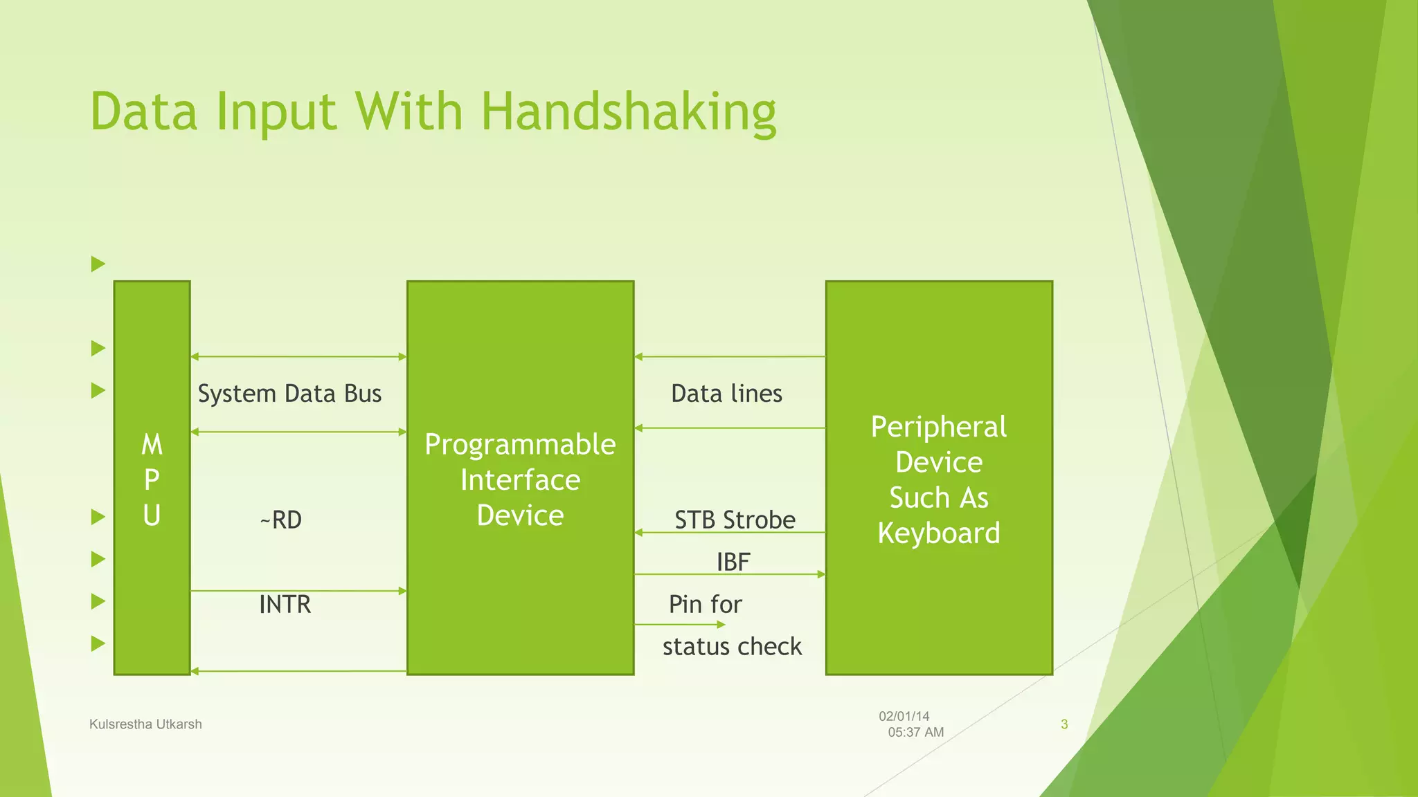
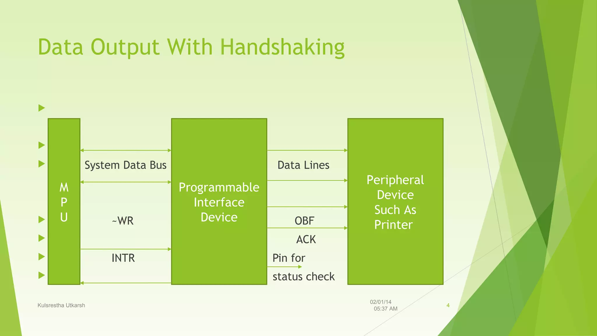


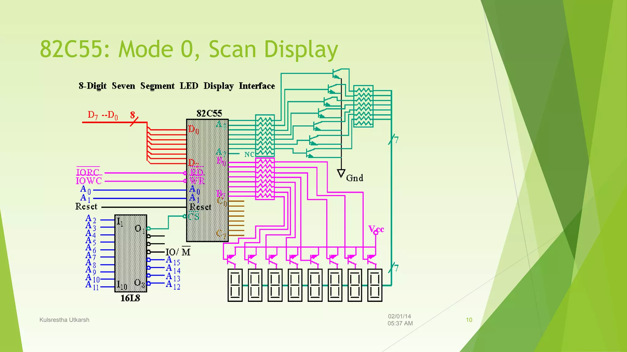


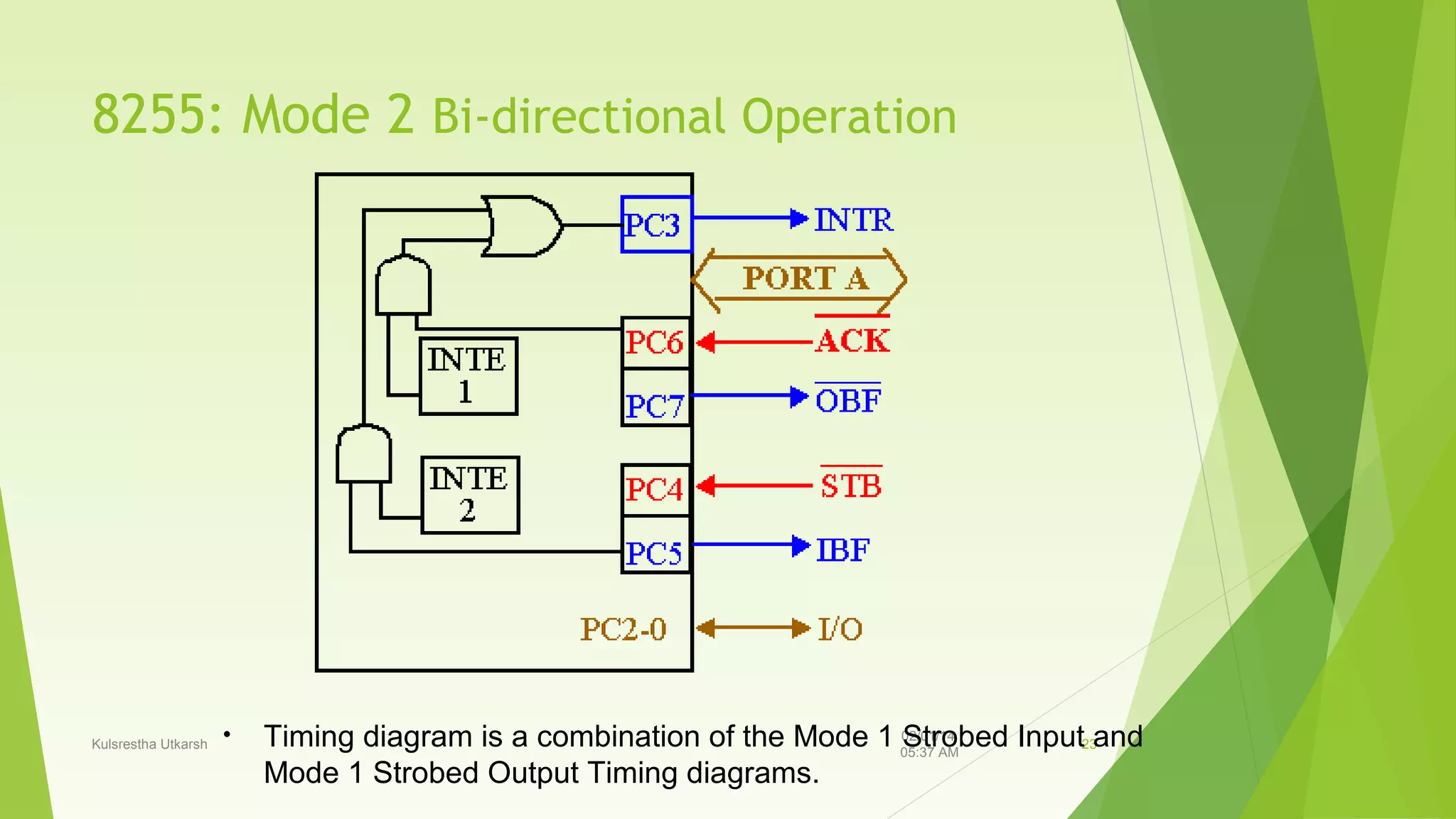


The document details the 8255 programmable peripheral interface, including its functions, pin layout, and operational modes. It describes three distinct modes of operation: Mode 0 for simple input/output, Mode 1 for input/output with handshaking, and Mode 2 for bi-directional communication. Additionally, it covers programming specifics and signal definitions necessary for interfacing with various peripheral devices.