Downloaded 1,563 times


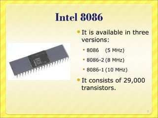
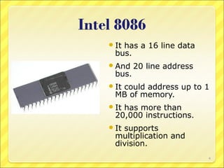

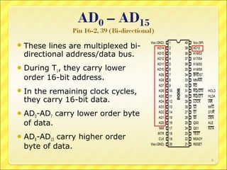


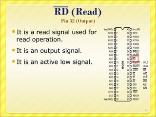


The document describes the Intel 8086 microprocessor, which was launched in 1978 as the first 16-bit microprocessor. It had major improvements over the 8085 microprocessor, with higher execution speeds. The 8086 had a 16-bit data bus, 20-bit address bus, and could address up to 1MB of memory. It included features like multiplication and division support. The document provides detailed information on the various pins and signals of the 8086 microprocessor.