Microprocessor Interfacing and 8155 Features
•Download as DOCX, PDF•
3 likes•11,762 views

In what way 8155 and 8156 differs and 8155 features

Recommended
More Related Content
What's hot
What's hot (20)
Viewers also liked
Similar to Microprocessor Interfacing and 8155 Features
Similar to Microprocessor Interfacing and 8155 Features (20)
More from Srikrishna Thota
More from Srikrishna Thota (19)
Recently uploaded
Recently uploaded (20)
Microprocessor Interfacing and 8155 Features
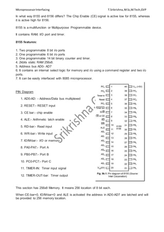
- 1. MicroprossesorInterfacing T.Srikrishna,M.Sc,M.Tech,GVP In what way 8155 and 8156 differs? The Chip Enable (CE) signal is active low for 8155, whereas it is active high for 8156. 8155 is a multifunction or Multipurpose Programmable device. It contains RAM, I/O port and timer. 8155 features: 1. Two programmable 8 bit i/o ports 2. One programmable 6 bit i/o ports 3. One programmable 14 bit binary counter and timer. 4. 2kbits static RAM 256x8. 5. Address bus AD0- AD7 6. It contains an internal select logic for memory and i/o using a command register and two i/o ports. 7. It can be easily interfaced with 8085 microprocessor. PIN Diagram 1. AD0-AD: - Address/Data bus multiplexed 2. RESET:- RESET input 3. CE bar:- chip enable 4. ALE:- Arithmetic latch enable 5. RD-bar:- Read input 6. WR-bar:- Write input 7. IO/M-bar:- I/O or memory 8. PA0-PA7:- Port A 9. PB0-PB7:- Port B 10. PC0-PC7:- Port C 11. TIMER-IN: Timer input signal 12. TIMER-OUT-bar: Timer output This section has 256x8 Memory. It means 256 location of 8 bit each. When CE-bar=0, IO/M-bar=0 and ALE is activated the address in AD0-AD7 are latched and will be provided to 256 memory location.
- 2. MicroprossesorInterfacing T.Srikrishna,M.Sc,M.Tech,GVP A2 A1 A0 Port 0 0 0 Command/status reg. 0 0 1 PA 0 1 0 PB 0 1 1 PC 1 0 0 Timer LSB 1 0 1 Timer MSB D7 D6 D5 D4 D3 D2 D1 D0 Timer command IEB IEA PC (ALT1 and ALT0) PB PA Control register also called command register. It is a 8-bit which defines different functions. It defines the function of different ports such as input, output or handshaking mode. It also defines timer command for timer to start and stop. The different combinations on the address lines A2, A1, A0 select one of the above, as shown: A2 0 A1 0 A0 0 ===>> Control/Status Register 0 0 1 ===>> Port A 0 1 0 ===>> Port B 0 1 1 ===>> Port C 1 0 0 ===>> LSB Timer 1 0 1 ===>> MSB Timer It is to be noted that the control/status register is having the same address 20H, But the control register is accessed with WR’ = 0 and RD’ = 1. For status register access, WR’= 1 and RD’ = 0. The control register can never be read.
- 3. MicroprossesorInterfacing T.Srikrishna,M.Sc,M.Tech,GVP The other five (viz., A7 to A3) on the address lines are as: 0 0 1 0 0. Thus A7 0 A6 0 A5 1 A4 0 A3 0 A2 0 A1 0 A0 0 ===>> Address 20H — Register/Port/Timer Control/Status register 0 0 1 0 0 0 0 1 ===>> 21H — Port A 0 0 1 0 0 0 1 0 ===>> 22H — Port B 0 0 1 0 0 0 1 1 ===>> 23H — Port C 0 0 1 0 0 1 0 0 ===>> 24H — LSB timer 0 0 1 0 0 1 0 1 ===>> 25H — MSB timer The control register contains eight bits. The content of the lower 2 bits, D1 – D0 configure ports A and B as input/output.
- 4. MicroprossesorInterfacing T.Srikrishna,M.Sc,M.Tech,GVP Bits D3 and D2 configure bits PC0 – PC5 of port C (Port C is a 6-bit port while ports A and B both are of 8-bits) and can have four combinations—ALT1, ALT2, ALT3, ALT4 depending on the combinations of D3 and D2. Bits D5 and D4 are enable/disable pins for ports A and B respectively which enable/ disable the internal flip-flop of 8155. Bits D7 and D6 contain the timer commands. As already mentioned, combinations of D3 – D2 bits give rise to ALT1 to ALT4 modes, which assigns port C bits in different configurations and shown below Port C pin assignment Pin ALT1 ALT2 ALT3 ALT4 PC0 PC1 PC2 PC3 PC4 PC5 Input Port Input Port Input Port Input Port Input Port Input Port Output Port Output Port Output Port Output Port Output Port Output Port A INTR (Port A Interrupt) A BF (Port A Buffer Full) A STB(Port A Strobe) Output Port Output Port Output Port A INTR (Port A Interrupt) A BF (Port A Buffer Full) A STB(Port A Strobe) B INTR (Port B Interrupt) B BF (Port Buffer Full) B STB(Port B Strobe) ALT1 and ALT2 correspond to simple input/output of Port C respectively. In ALT3 mode, PC0 – PC2 bits are used as control signals for port A, while pins PC3 – PC5 act as output pins. In ALT4 mode, PC0 – PC2 bits are used as control signals for port A, while PC3 – PC5 bits are used as control signals for port B.
- 5. MicroprossesorInterfacing T.Srikrishna,M.Sc,M.Tech,GVP It has seven bits. Bit D7 is the ‘don’t care’ bit. Bit D6 contains the status of the timer. Bits D5 – D3 concern to status of port B while bits D2 – D0 to that of Port A. The 8155 timer consists of two 8-bit registers. 1. 8-bit LSB and 8-bit MSB. 2. In these 16 bits, 14 bits are used for counter and two bits (M2 and M1) for mode selection. 3. The counter is a 14 bit down counter. It can operate in 4 different modes of operation. Timer MSB: M2 M1 T13 T12 T11 T10 T9 T8 Timer LSB: T7 T6 T5 T4 T3 T2 T1 T0 Mode 0: In this mode, timer gives only one cycle of square wave, the output remains high for 1/2 count and remain s low for 1/2 count. Wave width depends on two factor: one is Input clock pulse frequency, and the other is count loaded in counter. Mode 1: This mode is similar to single square wave in operation but the when counter becomes zero, the count value is automatically reloaded. Thus it provides continuous square wave. Mode 2: This mode gives a single clock pulse as a output of the end of the count. The output is high normally, but it becomes low for 1 clock pulse and again it will become high and remain high. Mode 3: This mode is similar to mode 2 but when the counter becomes zero the count value is automatically reloaded. Thus it provides continuous pulses.