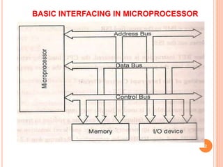
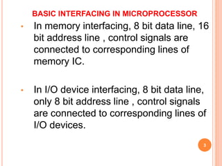
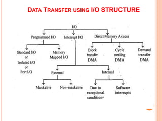
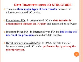
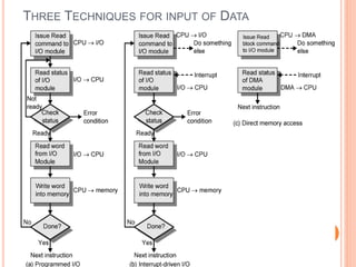
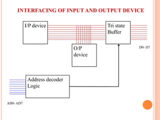
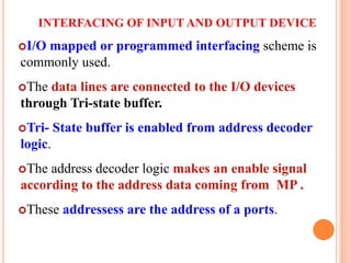
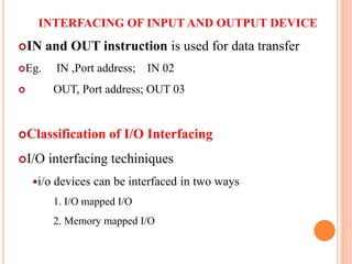
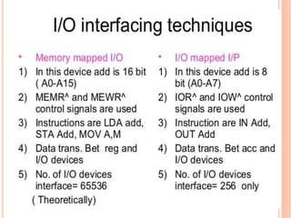
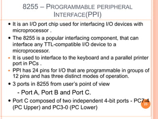
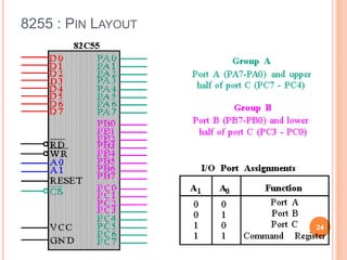
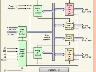
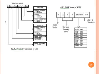
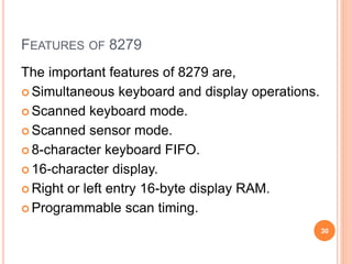
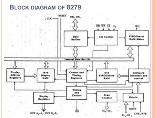
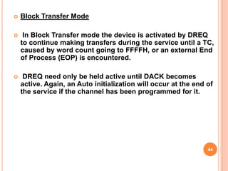
MEMORY AND I/O INTERFACING
CHAPTER -5
1
BASIC INTERFACING IN MICROPROCESSOR
2
BASIC INTERFACING IN MICROPROCESSOR
• In memory interfacing, 8 bit data line, 16
bit address line , control signals are
connected to corresponding lines of
memory IC.
• In I/O device interfacing, 8 bit data line,
only 8 bit address line , control signals
are connected to corresponding lines of
I/O devices.
3
DATA TRANSFER USING I/O STRUCTURE
4
DATA TRANSFER USING I/O STRUCTURE
 There are three major types of data transfer between the
microprocessor and I/O device.
 Programmed I/O : In programmed I/O the data transfer is
accomplished through an I/O port and controlled by software.
 Interrupt driven I/O : In interrupt driven I/O, the I/O device will
interrupt the processor, and initiate data transfer.
 Direct memory access (DMA) : In DMA, the data transfer
between memory and I/O can be performed by bypassing the
microprocessor.
5
THREE TECHNIQUES FOR INPUT OF DATA
6
INTERFACING I/O DEVICES
DEEPAK.P7
7
INTERFACING OF INPUT AND OUTPUT DEVICE
8
I/P device
O/P
device
Tri state
Buffer
Address decoder
Logic
AD0- AD7
D0- D7
INTERFACING OF INPUT AND OUTPUT DEVICE
I/O mapped or programmed interfacing scheme is
commonly used.
The data lines are connected to the I/O devices
through Tri-state buffer.
Tri- State buffer is enabled from address decoder
logic.
The address decoder logic makes an enable signal
according to the address data coming from MP .
These addressess are the address of a ports.
9
INTERFACING OF INPUT AND OUTPUT DEVICE
IN and OUT instruction is used for data transfer
Eg. IN ,Port address; IN 02
 OUT, Port address; OUT 03
Classification of I/O Interfacing
I/O interfacing techiniques
i/o devices can be interfaced in two ways
1. I/O mapped I/O
2. Memory mapped I/O
10
11
I/O DEVICE INTERFACE
 An I/O device interface is a circuit between
a device and the interconnection network
 Provides the means for data transfer and
exchange of status and control information
 Includes data, status, and control registers
accessible with Load and Store instructions
 Memory-mapped I/O enables software to view these
registers as locations in memory
12
13
DATA COMMUNICATION
 When data is transmitted between two piece of
equipment, 3 modes of communication are used
1. Simplex
Data is transmitted in one direction only
Only one wire is needed to connect the two devices
2.Half Duplex
This is used when to devices wants information
alternatively, but one after another .
One wire is sufficient.
3. Full Duplex
This is used when data is to be exchanged between
two devices in both directions simultaneously
Two wires are needed. 14
 Serial
 Cheaper
 Slower
 Parallel
 Faster
 Data skew
 Limited to
small distances
Data
Transmission
Parallel Serial
Synchronous ASynchronous15
 Synchronous Data Transmission
• The transmitter and receiver are synchronized.
– A sequence of synchronization signals is sent
before the communication begins.
 Asynchronous Data Transmission
• Transmission occurs at any time.
• Character based.
– Each character is sent separately
16
 Programmable chip 8251
 Requirement of HW control serial I/O
 An input/output port is required for interfacing
 Converts data bits in to Parallel to serial & vice versa
 Data transfer to be synchronized between I/O
 USART (Universal Synchronous Asynchronous
Receiver and Transmitter )
17
 Writing a program compatible with all different
serial communication protocols is difficult and it is
an inefficient use of microprocessor.
 UART: Universal Asynchronous receiver/
Transmitter chip.
 USART: Universal Synchronous/Asynchronous
Receiver/Transmitter chip.
 The microprocessor sends/receives the data to
the UART in parallel, while with I/O, the UART
transmits/receive data serially.
 8251 functions are integrated into standard PC
interface chip.
18
Data Bus
Buffer
Transmit
Buffer
Receive
Buffer
Transmit
Control
Receive
Control
R/W
Control
Logic
Modem
Control
I
n
t
e
r
n
a
l
L
i
n
e
D7-D0
RESET
CLK
C/Db
RDb
WRb
CSb
DSRb
DTRb
CTSb
RTSb
TXD
TXRDY
TXE
TXC
RXD
RXRDY
RXC
SYBDET/BD
19
CSb C/Db RDb WRb Meaning
1 X X X Data Bus Tri-state
0 X 1 1 Data Bus Tri-state
0 1 0 1 Status  CPU
0 1 1 0 Control Word CPU
0 0 0 1 Data  CPU (accept
data from Data Buffer)
0 0 1 0 Data  CPU (Out put
data to Data buffer) 20
D0 – D7 : This is an 8-bit data bus used to read or write status, command
word or data from or to the 8251.
C / D : (Control Word/Data): This input pin, together with RD and WR
inputs, informs the 8251 that the word on the data bus is either a data or
control word/status information. If this pin is 1, control / status is on the
bus, otherwise data is on the bus.
RD : This active-low input to 8251 is used to inform it that the CPU is
reading either data or status information from its internal registers.
WR : This is an active-low chip select input of 825l. If it is high, no read or
write operation can be carried out on 8251.
CLK : This input is used to generate internal device timings and is
normally connected to clock generator output.
RESET : A high on this input forces the 8251 into an idle state.
TXC (Transmitter Clock Input) : This transmitter clock input controls the
rate at which the character is to be transmitted.
TXD (Transmitted Data Output) : This output pin carries serial stream of
the transmitted data bits.
RXC (Receiver Clock Input) : This receiver clock input pin controls the
rate at which the character is to be received.
21
RXD (Receive Data Input) : This input pin of 8251A receives a
composite stream of the data to be received by 8251 .
RXRDY (Receiver Ready Output) : This output indicates that the
8251 contains a character to be read by the CPU.
TXRDY - Transmitter Ready : This output signal indicates to the
CPU that the internal circuit of the transmitter is ready to accept a
new character for transmission from the CPU.
DSR - Data Set Ready : This is normally used to check if data set is
ready when communicating with a modem
DTR - Data Terminal Ready : This is used to indicate that the device
is ready to accept data when the 8251 is communicating with a
modem.
RTS - Request to Send Data : This signal is used to communicate
with a modem.
TXE- Transmitter Empty : The TXE signal can be used to indicate
the end of a transmission mode.
22
8255 – PROGRAMMABLE PERIPHERAL
INTERFACE(PPI)
 It is an I/O port chip used for interfacing I/O devices with
microprocessor .
 The 8255 is a popular interfacing component, that can
interface any TTL-compatible I/O device to a
microprocessor.
 It is used to interface to the keyboard and a parallel printer
port in PCs .
 PPI has 24 pins for I/O that are programmable in groups of
12 pins and has three distinct modes of operation.
 3 ports in 8255 from user’s point of view
- Port A, Port B and Port C.
 Port C composed of two independent 4-bit ports - PC7-4
(PC Upper) and PC3-0 (PC Lower)
23
8255 : PIN LAYOUT
24
25
There is also a Control port from the Processor point of
view. Its contents decides the working of 8255.
Control logic of 8255:
RD (read): this signal enables the read operation. When
the signal is low , microprocessor reads data from a
selected I/O port of 8255.
WR (write) : this control signal enables the write operation.
RESET : It clears the control registers and sets all ports in
input mode.
CS , A0,A1 : these are device select signals connected
to a decoded address and A0,A1 are connected to
A0,A1 of microprocessor.
Port A, Port B, Port C and Control port will have the
addresses as 7CH, 7DH, 7EH, and 7FH respectively.
26
27
8255 can be used in two modes:
Bit set/Reset (BSR) mode:
The BSR mode is used to set or rest the bits in port C.
Input / Output mode:
I/O mode operates in 3 modes :
mode 0, mode 1, mode 2
Mode 0: Simple Input or Output
Mode 1: Input or Output with Handshake
Mode 2: port A can be set up for Bidirectional Data Transfer
using handshake signals from port C, and port B can be set
up either in mode0 or mode 1.
28
KEYBOARD/DISPLAY
CONTROLLER - INTEL 8279
29
FEATURES OF 8279
The important features of 8279 are,
 Simultaneous keyboard and display operations.
 Scanned keyboard mode.
 Scanned sensor mode.
 8-character keyboard FIFO.
 16-character display.
 Right or left entry 16-byte display RAM.
 Programmable scan timing.
30
BLOCK DIAGRAM OF 8279
31
The Keyboard display controller chip 8279 provides
1. A set of four scan lines and eight return lines for interfacing
keyboards.
2. A set of eight output lines for interfacing display.
 I/O Control and Data Buffer
 The I/O control section controls the flow of data to/from the
8279.
 The data buffer interface the external bus of the system with
internal bus of 8279.
 The I/O section is enabled only if D is low.
 The pin Ao, RD and WR select the command, status or data
read/write operations carried out by the CPU with 8279.
32
 Control and Timing Register and Timing Control
 These registers store the keyboard and display modes and
other operating conditions programmed by CPU. The
registers are written with Ao=1 and WR =0.
 The timing and control unit controls the basic timings for the
operation of the circuit. Scan Counter divide down the
operating frequency of 8279 to derive scan keyboard and
scan display frequencies.
 Scan Counter
 The Scan Counter has two modes to scan the key matrix and
refresh the display.
 In the Encoded mode, the counter provides a binary count
that is to be externally decoded to provide the scan lines for
keyboard and display In the decoded scan mode, the counter
internally decodes the least significant 2 bits and provides a
decoded 1 out of 4 scan on SL0-SL3 The Keyboard and
Display both are in the same mode at a time.
33
 Modes of Operation of 8279
 The Modes of operation of 8279 are
i. Input (Keyboard) modes
ii. Output (Display) modes
 Input (Keyboard) modes :
8279 provides three input modes, they are :
1. Scanned Keyboard Mode :
 This mode allows a key matrix to be interfaced using either
encoded or decoded scans.
 In the encoded scan, an 8 x 8 keyboard or in decoded
scan , a 4 x 8 Keyboard can be interfaced. The code of key
pressed with SHIFT and CONTROL status is stored into
the FIFO RAM.
34
 2. Scanned Sensor Matrix:
 In this mode, a sensor array can be interfaced with 8279
using either encoder or decoder scans. With encoder scan 8
x 8 sensor matrix or with decoder scan 4 x 8 sensor matrix
can be interfaced . The sensor codes are stored in the CPU
addressable sensor RAM.
 3. Strobed Input :
In this mode, if the control line goes low, the data on
return lines, is stored in the FIFO byte by byte.
 Output (Display) Modes :
8279 provides two output modes for selecting the display
options.
 1. Display Scan:
 In this mode, 8279 provides 8 or 16 character multiplexed
displays those can be organized as dual 4-bit or single 8-bit
display units.
35
 2. Display Entry:
 The Display data is entered for display either from the right
side or from the left side.
36
8237 –DMA CONTOLLERS
 DMA Definitions:
 DMA occurs between an I/O device and memory
without the use of the microprocessor
 DMA read transfer data from the memory to I/O
device
 DMA write transfer data from the I/O to memory
 MRDC & IOWC signals to simultaneously activate
for read DMA
37
BASIC DMA OPERATION
 The direct memory access (DMA) I/O technique provides
direct access to the memory while the microprocessor is
temporarily disabled.
 A DMA controller temporarily borrows the address bus,
data bus, and control bus from the microprocessor and
transfers the data bytes directly between an I/O port and a
series of memory locations.
 The DMA transfer is also used to do high-speed memory-to
memory transfers.
 Two control signals are used to request and acknowledge a
DMA transfer in the microprocessor-based system.
38
 The HOLD signal is a bus request signal which asks
the microprocessor to release control of the buses
after the current bus cycle.
 The HLDA signal is a bus grant signal which
indicates that the microprocessor has indeed
released control of its buses by placing the buses at
their high-impedance states.
 The HOLD input has a higher priority than the INTR
or NMI interrupt inputs.
39
THE 8237 DMA CONTROLLER
 The 8237 DMA controller supplies the
memory and I/O with control signals and
memory address information during the
DMA transfer.
 The 8237 is capable of DMA transfers at
rates of up to 1.6M bytes per second.
 Each channel is capable of addressing a
full 64K-byte section of memory and can
transfer up to 64K bytes with a single
programming. 40
SOME IMPORTANT SIGNAL PINS
 DREQ3 – DREQ0 (DMA request): Used
to request a DMA transfer for a
particular DMA channel.
• DACK3 – DACK0 (DMA channel
acknowledge): Acknowledges a
channel DMA request from a device.
• HRQ (Hold request): Requests a DMA
transfer.
• HLDA (Hold acknowledge) signals the
8237 that the microprocessor has
relinquished control of the address,
data and control buses. 41
 MEMW (Memory write): Used as an output to cause
memory to write data during a DMA write cycle.
 MEMR (Memory read): Used as an output to cause
memory to read data during a DMA read cycle
 A3 – A0 : address pins select an internal register during
programming and provide part of the DMA transfer
address during DMA operation.
 A7 – A4 : address pins are outputs that provide part of the
DMA transfer address during a DMA operation.
 DB0 – DB7 : data bus, connected to microprocessor and
are used during the programming DMA controller.
42
DATA TRANSFER MODES
 Single Transfer Mode
 In Single Transfer mode the device is programmed to
make one transfer only.
 The word count will be decremented and the address
decremented or incremented following each transfer.
 When the word count ``rolls over'' from zero to
FFFFH, a Terminal Count (TC) will cause an Auto
initialize if the channel has been programmed to do
so.
43
 Block Transfer Mode
 In Block Transfer mode the device is activated by DREQ
to continue making transfers during the service until a TC,
caused by word count going to FFFFH, or an external End
of Process (EOP) is encountered.
 DREQ need only be held active until DACK becomes
active. Again, an Auto initialization will occur at the end of
the service if the channel has been programmed for it.
44

Chapter5

  • 1.
    MEMORY AND I/OINTERFACING CHAPTER -5 1
  • 2.
    BASIC INTERFACING INMICROPROCESSOR 2
  • 3.
    BASIC INTERFACING INMICROPROCESSOR • In memory interfacing, 8 bit data line, 16 bit address line , control signals are connected to corresponding lines of memory IC. • In I/O device interfacing, 8 bit data line, only 8 bit address line , control signals are connected to corresponding lines of I/O devices. 3
  • 4.
    DATA TRANSFER USINGI/O STRUCTURE 4
  • 5.
    DATA TRANSFER USINGI/O STRUCTURE  There are three major types of data transfer between the microprocessor and I/O device.  Programmed I/O : In programmed I/O the data transfer is accomplished through an I/O port and controlled by software.  Interrupt driven I/O : In interrupt driven I/O, the I/O device will interrupt the processor, and initiate data transfer.  Direct memory access (DMA) : In DMA, the data transfer between memory and I/O can be performed by bypassing the microprocessor. 5
  • 6.
    THREE TECHNIQUES FORINPUT OF DATA 6
  • 7.
  • 8.
    INTERFACING OF INPUTAND OUTPUT DEVICE 8 I/P device O/P device Tri state Buffer Address decoder Logic AD0- AD7 D0- D7
  • 9.
    INTERFACING OF INPUTAND OUTPUT DEVICE I/O mapped or programmed interfacing scheme is commonly used. The data lines are connected to the I/O devices through Tri-state buffer. Tri- State buffer is enabled from address decoder logic. The address decoder logic makes an enable signal according to the address data coming from MP . These addressess are the address of a ports. 9
  • 10.
    INTERFACING OF INPUTAND OUTPUT DEVICE IN and OUT instruction is used for data transfer Eg. IN ,Port address; IN 02  OUT, Port address; OUT 03 Classification of I/O Interfacing I/O interfacing techiniques i/o devices can be interfaced in two ways 1. I/O mapped I/O 2. Memory mapped I/O 10
  • 11.
  • 12.
    I/O DEVICE INTERFACE An I/O device interface is a circuit between a device and the interconnection network  Provides the means for data transfer and exchange of status and control information  Includes data, status, and control registers accessible with Load and Store instructions  Memory-mapped I/O enables software to view these registers as locations in memory 12
  • 13.
  • 14.
    DATA COMMUNICATION  Whendata is transmitted between two piece of equipment, 3 modes of communication are used 1. Simplex Data is transmitted in one direction only Only one wire is needed to connect the two devices 2.Half Duplex This is used when to devices wants information alternatively, but one after another . One wire is sufficient. 3. Full Duplex This is used when data is to be exchanged between two devices in both directions simultaneously Two wires are needed. 14
  • 15.
     Serial  Cheaper Slower  Parallel  Faster  Data skew  Limited to small distances Data Transmission Parallel Serial Synchronous ASynchronous15
  • 16.
     Synchronous DataTransmission • The transmitter and receiver are synchronized. – A sequence of synchronization signals is sent before the communication begins.  Asynchronous Data Transmission • Transmission occurs at any time. • Character based. – Each character is sent separately 16
  • 17.
     Programmable chip8251  Requirement of HW control serial I/O  An input/output port is required for interfacing  Converts data bits in to Parallel to serial & vice versa  Data transfer to be synchronized between I/O  USART (Universal Synchronous Asynchronous Receiver and Transmitter ) 17
  • 18.
     Writing aprogram compatible with all different serial communication protocols is difficult and it is an inefficient use of microprocessor.  UART: Universal Asynchronous receiver/ Transmitter chip.  USART: Universal Synchronous/Asynchronous Receiver/Transmitter chip.  The microprocessor sends/receives the data to the UART in parallel, while with I/O, the UART transmits/receive data serially.  8251 functions are integrated into standard PC interface chip. 18
  • 19.
  • 20.
    CSb C/Db RDbWRb Meaning 1 X X X Data Bus Tri-state 0 X 1 1 Data Bus Tri-state 0 1 0 1 Status  CPU 0 1 1 0 Control Word CPU 0 0 0 1 Data  CPU (accept data from Data Buffer) 0 0 1 0 Data  CPU (Out put data to Data buffer) 20
  • 21.
    D0 – D7: This is an 8-bit data bus used to read or write status, command word or data from or to the 8251. C / D : (Control Word/Data): This input pin, together with RD and WR inputs, informs the 8251 that the word on the data bus is either a data or control word/status information. If this pin is 1, control / status is on the bus, otherwise data is on the bus. RD : This active-low input to 8251 is used to inform it that the CPU is reading either data or status information from its internal registers. WR : This is an active-low chip select input of 825l. If it is high, no read or write operation can be carried out on 8251. CLK : This input is used to generate internal device timings and is normally connected to clock generator output. RESET : A high on this input forces the 8251 into an idle state. TXC (Transmitter Clock Input) : This transmitter clock input controls the rate at which the character is to be transmitted. TXD (Transmitted Data Output) : This output pin carries serial stream of the transmitted data bits. RXC (Receiver Clock Input) : This receiver clock input pin controls the rate at which the character is to be received. 21
  • 22.
    RXD (Receive DataInput) : This input pin of 8251A receives a composite stream of the data to be received by 8251 . RXRDY (Receiver Ready Output) : This output indicates that the 8251 contains a character to be read by the CPU. TXRDY - Transmitter Ready : This output signal indicates to the CPU that the internal circuit of the transmitter is ready to accept a new character for transmission from the CPU. DSR - Data Set Ready : This is normally used to check if data set is ready when communicating with a modem DTR - Data Terminal Ready : This is used to indicate that the device is ready to accept data when the 8251 is communicating with a modem. RTS - Request to Send Data : This signal is used to communicate with a modem. TXE- Transmitter Empty : The TXE signal can be used to indicate the end of a transmission mode. 22
  • 23.
    8255 – PROGRAMMABLEPERIPHERAL INTERFACE(PPI)  It is an I/O port chip used for interfacing I/O devices with microprocessor .  The 8255 is a popular interfacing component, that can interface any TTL-compatible I/O device to a microprocessor.  It is used to interface to the keyboard and a parallel printer port in PCs .  PPI has 24 pins for I/O that are programmable in groups of 12 pins and has three distinct modes of operation.  3 ports in 8255 from user’s point of view - Port A, Port B and Port C.  Port C composed of two independent 4-bit ports - PC7-4 (PC Upper) and PC3-0 (PC Lower) 23
  • 24.
    8255 : PINLAYOUT 24
  • 25.
  • 26.
    There is alsoa Control port from the Processor point of view. Its contents decides the working of 8255. Control logic of 8255: RD (read): this signal enables the read operation. When the signal is low , microprocessor reads data from a selected I/O port of 8255. WR (write) : this control signal enables the write operation. RESET : It clears the control registers and sets all ports in input mode. CS , A0,A1 : these are device select signals connected to a decoded address and A0,A1 are connected to A0,A1 of microprocessor. Port A, Port B, Port C and Control port will have the addresses as 7CH, 7DH, 7EH, and 7FH respectively. 26
  • 27.
    27 8255 can beused in two modes: Bit set/Reset (BSR) mode: The BSR mode is used to set or rest the bits in port C. Input / Output mode: I/O mode operates in 3 modes : mode 0, mode 1, mode 2 Mode 0: Simple Input or Output Mode 1: Input or Output with Handshake Mode 2: port A can be set up for Bidirectional Data Transfer using handshake signals from port C, and port B can be set up either in mode0 or mode 1.
  • 28.
  • 29.
  • 30.
    FEATURES OF 8279 Theimportant features of 8279 are,  Simultaneous keyboard and display operations.  Scanned keyboard mode.  Scanned sensor mode.  8-character keyboard FIFO.  16-character display.  Right or left entry 16-byte display RAM.  Programmable scan timing. 30
  • 31.
  • 32.
    The Keyboard displaycontroller chip 8279 provides 1. A set of four scan lines and eight return lines for interfacing keyboards. 2. A set of eight output lines for interfacing display.  I/O Control and Data Buffer  The I/O control section controls the flow of data to/from the 8279.  The data buffer interface the external bus of the system with internal bus of 8279.  The I/O section is enabled only if D is low.  The pin Ao, RD and WR select the command, status or data read/write operations carried out by the CPU with 8279. 32
  • 33.
     Control andTiming Register and Timing Control  These registers store the keyboard and display modes and other operating conditions programmed by CPU. The registers are written with Ao=1 and WR =0.  The timing and control unit controls the basic timings for the operation of the circuit. Scan Counter divide down the operating frequency of 8279 to derive scan keyboard and scan display frequencies.  Scan Counter  The Scan Counter has two modes to scan the key matrix and refresh the display.  In the Encoded mode, the counter provides a binary count that is to be externally decoded to provide the scan lines for keyboard and display In the decoded scan mode, the counter internally decodes the least significant 2 bits and provides a decoded 1 out of 4 scan on SL0-SL3 The Keyboard and Display both are in the same mode at a time. 33
  • 34.
     Modes ofOperation of 8279  The Modes of operation of 8279 are i. Input (Keyboard) modes ii. Output (Display) modes  Input (Keyboard) modes : 8279 provides three input modes, they are : 1. Scanned Keyboard Mode :  This mode allows a key matrix to be interfaced using either encoded or decoded scans.  In the encoded scan, an 8 x 8 keyboard or in decoded scan , a 4 x 8 Keyboard can be interfaced. The code of key pressed with SHIFT and CONTROL status is stored into the FIFO RAM. 34
  • 35.
     2. ScannedSensor Matrix:  In this mode, a sensor array can be interfaced with 8279 using either encoder or decoder scans. With encoder scan 8 x 8 sensor matrix or with decoder scan 4 x 8 sensor matrix can be interfaced . The sensor codes are stored in the CPU addressable sensor RAM.  3. Strobed Input : In this mode, if the control line goes low, the data on return lines, is stored in the FIFO byte by byte.  Output (Display) Modes : 8279 provides two output modes for selecting the display options.  1. Display Scan:  In this mode, 8279 provides 8 or 16 character multiplexed displays those can be organized as dual 4-bit or single 8-bit display units. 35
  • 36.
     2. DisplayEntry:  The Display data is entered for display either from the right side or from the left side. 36
  • 37.
    8237 –DMA CONTOLLERS DMA Definitions:  DMA occurs between an I/O device and memory without the use of the microprocessor  DMA read transfer data from the memory to I/O device  DMA write transfer data from the I/O to memory  MRDC & IOWC signals to simultaneously activate for read DMA 37
  • 38.
    BASIC DMA OPERATION The direct memory access (DMA) I/O technique provides direct access to the memory while the microprocessor is temporarily disabled.  A DMA controller temporarily borrows the address bus, data bus, and control bus from the microprocessor and transfers the data bytes directly between an I/O port and a series of memory locations.  The DMA transfer is also used to do high-speed memory-to memory transfers.  Two control signals are used to request and acknowledge a DMA transfer in the microprocessor-based system. 38
  • 39.
     The HOLDsignal is a bus request signal which asks the microprocessor to release control of the buses after the current bus cycle.  The HLDA signal is a bus grant signal which indicates that the microprocessor has indeed released control of its buses by placing the buses at their high-impedance states.  The HOLD input has a higher priority than the INTR or NMI interrupt inputs. 39
  • 40.
    THE 8237 DMACONTROLLER  The 8237 DMA controller supplies the memory and I/O with control signals and memory address information during the DMA transfer.  The 8237 is capable of DMA transfers at rates of up to 1.6M bytes per second.  Each channel is capable of addressing a full 64K-byte section of memory and can transfer up to 64K bytes with a single programming. 40
  • 41.
    SOME IMPORTANT SIGNALPINS  DREQ3 – DREQ0 (DMA request): Used to request a DMA transfer for a particular DMA channel. • DACK3 – DACK0 (DMA channel acknowledge): Acknowledges a channel DMA request from a device. • HRQ (Hold request): Requests a DMA transfer. • HLDA (Hold acknowledge) signals the 8237 that the microprocessor has relinquished control of the address, data and control buses. 41
  • 42.
     MEMW (Memorywrite): Used as an output to cause memory to write data during a DMA write cycle.  MEMR (Memory read): Used as an output to cause memory to read data during a DMA read cycle  A3 – A0 : address pins select an internal register during programming and provide part of the DMA transfer address during DMA operation.  A7 – A4 : address pins are outputs that provide part of the DMA transfer address during a DMA operation.  DB0 – DB7 : data bus, connected to microprocessor and are used during the programming DMA controller. 42
  • 43.
    DATA TRANSFER MODES Single Transfer Mode  In Single Transfer mode the device is programmed to make one transfer only.  The word count will be decremented and the address decremented or incremented following each transfer.  When the word count ``rolls over'' from zero to FFFFH, a Terminal Count (TC) will cause an Auto initialize if the channel has been programmed to do so. 43
  • 44.
     Block TransferMode  In Block Transfer mode the device is activated by DREQ to continue making transfers during the service until a TC, caused by word count going to FFFFH, or an external End of Process (EOP) is encountered.  DREQ need only be held active until DACK becomes active. Again, an Auto initialization will occur at the end of the service if the channel has been programmed for it. 44

Editor's Notes

  • #14 Example i/o interface