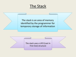
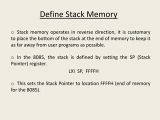
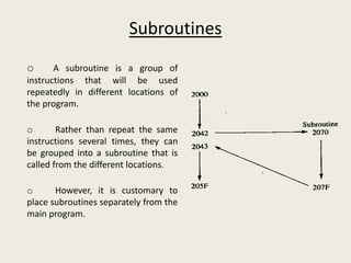
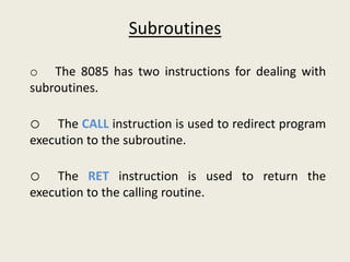
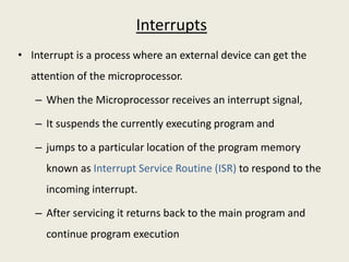
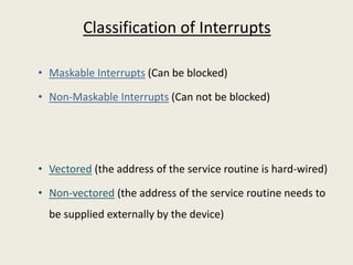
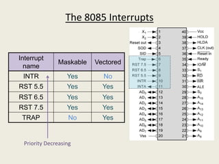
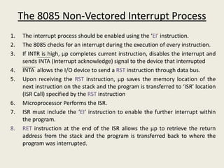
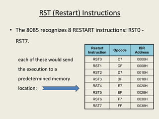
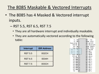
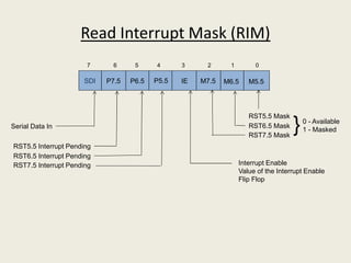
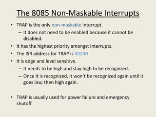
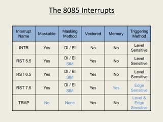
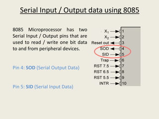
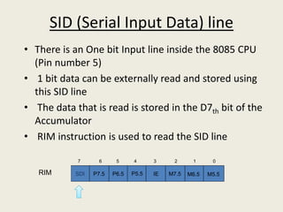
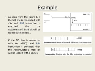
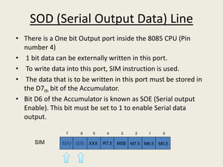
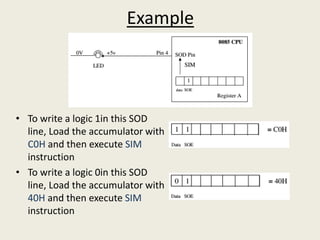
1. Stack and Subroutine
2. Interrupt and Serial Communication
The Stack
The stack uses a LIFO (Last In
First Out) structure
The stack is an area of memory
identified by the programmer for
temporary storage of information
o Stack memory operates in reverse direction, it is customary
to place the bottom of the stack at the end of memory to keep it
as far away from user programs as possible.
o In the 8085, the stack is defined by setting the SP (Stack
Pointer) register.
LXI SP, FFFFH
o This sets the Stack Pointer to location FFFFH (end of memory
for the 8085).
Define Stack Memory
o The 8085 provides two instructions: PUSH and POP
for storing information on the stack and retrieving
it back.
o Both PUSH and POP work with register pairs only.
Communication with Stack
PUSH Instruction POP Instruction Operation with
PUSH B POP B B – C Register pair
PUSH D POP D D – E Register pair
PUSH H POP H H – L Register pair
PUSH PSW POP PSW Accumulator and Flag
The PUSH Instruction
• PUSH B
 Decrement SP by 1
 Copy the contents of register B to the memory location pointed by
SP
 Decrement SP by 1
 Copy the contents of register C to the memory location pointed by
SP
The POP Instruction
• POP D
 Copy the contents of the memory location pointed to by the SP to
register E
 Increment SP by 1
 Copy the contents of the memory location pointed to by the SP to
register D
 Increment SP by 1
The PSW Register Pair
o The 8085 recognizes one additional register pair called the
PSW (Program Status Word).
o This register pair is made up of the Accumulator and the
Flags registers.
o It is possible to manipulate flag register using stack memory
concept.
Acc FlagPSW =
Some special instructions
• SPHL
Content of H-L pair are transferred to the stack pointer
• XTHL
Exchange the content of H-L pair with top of the Stack
A2 57
8097SP
H L
67
38
8098
8097
67 38
8097SP
H L
A2
57
8098
8097
Subroutines
o A subroutine is a group of
instructions that will be used
repeatedly in different locations of
the program.
o Rather than repeat the same
instructions several times, they can
be grouped into a subroutine that is
called from the different locations.
o However, it is customary to
place subroutines separately from the
main program.
Subroutines
o The 8085 has two instructions for dealing with
subroutines.
o The CALL instruction is used to redirect program
execution to the subroutine.
o The RET instruction is used to return the
execution to the calling routine.
Subroutines
Call & Return Instructions
2000H Instruction 1
2001H Instruction 2
2002H .
2003H .
2004H CALL 4020H
2005H
2006H
2007H .
2008H .
2009H .
200AH .
200BH .
200CH .
200DH .
200EH .
4020H Instruction 1
4021H Instruction 2
4022H .
4023H .
4024H .
4025H .
4026H .
4027H .
4028H .
4029H .
402AH .
402BH RET
The CALL Instruction
• CALL 4000H
o 3-byte instruction.
o Push the address of the instruction immediately following the
CALL onto the stack and decrement the stack pointer register by
two.
o Load the program counter with the 16-bit address supplied with
the CALL instruction.
o Jump Unconditionally to memory location.
Timing Diagram of CALL Instruction
• RET
o 1-byte instruction
o Retrieve the return address from the top of the stack and
increments stack pointer register by two.
o Load the program counter with the return address.
o Unconditionally returns from a subroutine.
The RET Instruction
RET
Conditional CALL Instruction
• CP <16-Bit Address> call when s = 0
• CM <16-Bit Address> call when s = 1
• CZ <16-Bit Address> call when z = 1
• CNZ <16-Bit Address> call when z = 0
• CPE <16-Bit Address> call when P = 1
• CPO <16-Bit Address> call when P = 0
• CC <16-Bit Address> call when CY = 1
• CNC <16-Bit Address> call when CY = 0
Conditional RETURN Instruction
• RP <16-Bit Address> return when s = 0
• RM <16-Bit Address> return when s = 1
• RZ <16-Bit Address> return when z = 1
• RNZ <16-Bit Address> return when z = 0
• RPE <16-Bit Address> return when P = 1
• RPO <16-Bit Address> return when P = 0
• RC <16-Bit Address> return when CY = 1
• RNC <16-Bit Address> return when CY = 0
Interrupts
Interrupts
• Interrupt is a process where an external device can get the
attention of the microprocessor.
– When the Microprocessor receives an interrupt signal,
– It suspends the currently executing program and
– jumps to a particular location of the program memory
known as Interrupt Service Routine (ISR) to respond to the
incoming interrupt.
– After servicing it returns back to the main program and
continue program execution
Classification of Interrupts
• Maskable Interrupts (Can be blocked)
• Non-Maskable Interrupts (Can not be blocked)
• Vectored (the address of the service routine is hard-wired)
• Non-vectored (the address of the service routine needs to
be supplied externally by the device)
The 8085 Interrupts
Interrupt
name
Maskable Vectored
INTR Yes No
RST 5.5 Yes Yes
RST 6.5 Yes Yes
RST 7.5 Yes Yes
TRAP No Yes
Priority Decreasing
1. The interrupt process should be enabled using the ‘EI’ instruction.
2. The 8085 checks for an interrupt during the execution of every instruction.
3. If INTR is high, μp completes current instruction, disables the interrupt and
sends INTA (Interrupt acknowledge) signal to the device that interrupted
4. INTA allows the I/O device to send a RST instruction through data bus.
5. Upon receiving the RST instruction, μp saves the memory location of the
next instruction on the stack and the program is transferred to ‘ISR’ location
(ISR Call) specified by the RST instruction
6. Microprocessor Performs the ISR.
7. ISR must include the ‘EI’ instruction to enable the further interrupt within
the program.
8. RET instruction at the end of the ISR allows the μp to retrieve the return
address from the stack and the program is transferred back to where the
program was interrupted.
The 8085 Non-Vectored Interrupt Process
RST (Restart) Instructions
• The 8085 recognizes 8 RESTART instructions: RST0 -
RST7.
Restart
Instruction
Opcode
ISR
Address
RST0 C7 0000H
RST1 CF 0008H
RST2 D7 0010H
RST3 DF 0018H
RST4 E7 0020H
RST5 EF 0028H
RST6 F7 0030H
RST7 FF 0038H
each of these would send
the execution to a
predetermined memory
location:
The 8085 Maskable & Vectored Interrupts
• The 8085 has 4 Masked & Vectored interrupt
inputs.
– RST 5.5, RST 6.5, RST 7.5
• They are all hardware interrupt and individually maskable.
• They are automatically vectored according to the following
table:
Interrupt ISR Address
RST 5.5 002CH
RST 6.5 0034H
RST 7.5 003CH
The 8085 Maskable & Vectored Interrupt Process
1. The interrupt process should be enabled using the EI instruction.
2. The 8085 checks for an interrupt during the execution of every
instruction.
3. If there is an interrupt, and if the corresponding interrupt pin is
enabled using the interrupt mask, the microprocessor will complete
the executing instruction, and reset the interrupt flip flop.
4. The microprocessor then saves the address of the next instruction on
the stack.
5. The microprocessor jumps to the specific service routine.
5. The service routine must include the instruction EI to re-enable the
interrupt process.
6. At the end of the service routine, the RET instruction returns the
execution to where the program was interrupted.
Set Interrupt Mask (SIM)
SDO SDE XX R7.5 MSE M7.5 M6.5 M5.5
01234567
RST5.5 Mask
RST6.5 Mask
RST7.5 Mask
}0 - Available
1 - Masked
Mask Set Enable
0 - Ignore bits 0-2
1 - Set the masks according
to bits 0-2
1 - Force RST7.5 Flip Flop to resetNot Used
Enable Serial Data
0 - Ignore bit 7
1 - Send bit 7 to SOD pin
Serial Data Out
Maskable Interrupts Hardware Logic
Interrupt
Enable
Flip Flop
INTR
RST 5.5
RST 6.5
RST 7.5
M 5.5
M 6.5
M 7.5
RST 7.5 Memory
Modify the Interrupt Masks Using the SIM Instruction
• Example: Set the interrupt masks so that RST5.5 and
RST7.5 are enabled, but RST6.5 is masked.
Content of accumulator is = 0 0 0 0 1 0 1 0 = 0A H
EI ; Enable interrupts including INTR
MVI A, 0A ; Prepare the mask to enable RST 7.5, and 5.5, disable 6.5
SIM ; Apply the settings RST masks
SDO SDE XXX R7.5 MSE M7.5 M6.5 M5.5
0 0 0 0 1 0 1 0
Serial
data is
ignored
Don’t
use serial
data
Bit 5 is
not used
Allow
setting
the
masks
Allow
setting
the
masks
Enable
7.5
Disable
6.5
Enable
5.5
Read Interrupt Mask (RIM)
SDI P7.5 P6.5 P5.5 IE M7.5 M6.5 M5.5
01234567
RST5.5 Mask
RST6.5 Mask
RST7.5 Mask
}0 - Available
1 - Masked
Interrupt Enable
Value of the Interrupt Enable
Flip Flop
Serial Data In
RST5.5 Interrupt Pending
RST6.5 Interrupt Pending
RST7.5 Interrupt Pending
The 8085 Non-Maskable Interrupts
• TRAP is the only non-maskable interrupt.
– It does not need to be enabled because it cannot be
disabled.
• It has the highest priority amongst interrupts.
• The ISR address for TRAP is 0024H
• It is edge and level sensitive.
– It needs to be high and stay high to be recognized.
– Once it is recognized, it won’t be recognized again until it
goes low, then high again.
• TRAP is usually used for power failure and emergency
shutoff.
The 8085 Interrupts
Interrupt
Name
Maskable
Masking
Method
Vectored Memory
Triggering
Method
INTR Yes DI / EI No No
Level
Sensitive
RST 5.5 Yes
DI / EI
SIM
Yes No
Level
Sensitive
RST 6.5 Yes
DI / EI
SIM
Yes No
Level
Sensitive
RST 7.5 Yes
DI / EI
SIM
Yes Yes
Edge
Sensitive
TRAP No None Yes No
Level &
Edge
Sensitive
Serial Data
Communication
Serial Input / Output data using 8085
8085 Microprocessor has two
Serial Input / Output pins that are
used to read / write one bit data
to and from peripheral devices.
Pin 4: SOD (Serial Output Data)
Pin 5: SID (Serial Input Data)
SID (Serial Input Data) line
• There is an One bit Input line inside the 8085 CPU
(Pin number 5)
• 1 bit data can be externally read and stored using
this SID line
• The data that is read is stored in the D7th bit of the
Accumulator
• RIM instruction is used to read the SID line
SDI P7.5 P6.5 P5.5 IE M7.5 M6.5 M5.5
01234567
RIM
Example
• As seen from the figure 1, if
the SID line is connected with
+5V and RIM instruction is
executed, then the
Accumulator’s MSB bit will be
loaded with a Logic 1
• if the SID line is connected
with 0V (GND) and RIM
instruction is executed, then
the Accumulator’s MSB bit
will be loaded with a Logic 0
SOD (Serial Output Data) Line
• There is a One bit Output port inside the 8085 CPU (Pin
number 4)
• 1 bit data can be externally written in this port.
• To write data into this port, SIM instruction is used.
• The data that is to be written in this port must be stored in
the D7th bit of the Accumulator.
• Bit D6 of the Accumulator is known as SOE (Serial output
Enable). This bit must be set to 1 to enable Serial data
output.
SDO SDE XXX R7.5 MSE M7.5 M6.5 M5.5
01234567
SIM
Example
• To write a logic 1in this SOD
line, Load the accumulator with
C0H and then execute SIM
instruction
• To write a logic 0in this SOD
line, Load the accumulator with
40H and then execute SIM
instruction

Microprocessor Part 4

  • 1.
    1. Stack andSubroutine 2. Interrupt and Serial Communication
  • 2.
    The Stack The stackuses a LIFO (Last In First Out) structure The stack is an area of memory identified by the programmer for temporary storage of information
  • 3.
    o Stack memoryoperates in reverse direction, it is customary to place the bottom of the stack at the end of memory to keep it as far away from user programs as possible. o In the 8085, the stack is defined by setting the SP (Stack Pointer) register. LXI SP, FFFFH o This sets the Stack Pointer to location FFFFH (end of memory for the 8085). Define Stack Memory
  • 4.
    o The 8085provides two instructions: PUSH and POP for storing information on the stack and retrieving it back. o Both PUSH and POP work with register pairs only. Communication with Stack PUSH Instruction POP Instruction Operation with PUSH B POP B B – C Register pair PUSH D POP D D – E Register pair PUSH H POP H H – L Register pair PUSH PSW POP PSW Accumulator and Flag
  • 5.
    The PUSH Instruction •PUSH B  Decrement SP by 1  Copy the contents of register B to the memory location pointed by SP  Decrement SP by 1  Copy the contents of register C to the memory location pointed by SP
  • 6.
    The POP Instruction •POP D  Copy the contents of the memory location pointed to by the SP to register E  Increment SP by 1  Copy the contents of the memory location pointed to by the SP to register D  Increment SP by 1
  • 7.
    The PSW RegisterPair o The 8085 recognizes one additional register pair called the PSW (Program Status Word). o This register pair is made up of the Accumulator and the Flags registers. o It is possible to manipulate flag register using stack memory concept. Acc FlagPSW =
  • 8.
    Some special instructions •SPHL Content of H-L pair are transferred to the stack pointer • XTHL Exchange the content of H-L pair with top of the Stack A2 57 8097SP H L 67 38 8098 8097 67 38 8097SP H L A2 57 8098 8097
  • 9.
  • 10.
    o A subroutineis a group of instructions that will be used repeatedly in different locations of the program. o Rather than repeat the same instructions several times, they can be grouped into a subroutine that is called from the different locations. o However, it is customary to place subroutines separately from the main program. Subroutines
  • 11.
    o The 8085has two instructions for dealing with subroutines. o The CALL instruction is used to redirect program execution to the subroutine. o The RET instruction is used to return the execution to the calling routine. Subroutines
  • 12.
    Call & ReturnInstructions 2000H Instruction 1 2001H Instruction 2 2002H . 2003H . 2004H CALL 4020H 2005H 2006H 2007H . 2008H . 2009H . 200AH . 200BH . 200CH . 200DH . 200EH . 4020H Instruction 1 4021H Instruction 2 4022H . 4023H . 4024H . 4025H . 4026H . 4027H . 4028H . 4029H . 402AH . 402BH RET
  • 13.
    The CALL Instruction •CALL 4000H o 3-byte instruction. o Push the address of the instruction immediately following the CALL onto the stack and decrement the stack pointer register by two. o Load the program counter with the 16-bit address supplied with the CALL instruction. o Jump Unconditionally to memory location.
  • 14.
    Timing Diagram ofCALL Instruction
  • 15.
    • RET o 1-byteinstruction o Retrieve the return address from the top of the stack and increments stack pointer register by two. o Load the program counter with the return address. o Unconditionally returns from a subroutine. The RET Instruction RET
  • 16.
    Conditional CALL Instruction •CP <16-Bit Address> call when s = 0 • CM <16-Bit Address> call when s = 1 • CZ <16-Bit Address> call when z = 1 • CNZ <16-Bit Address> call when z = 0 • CPE <16-Bit Address> call when P = 1 • CPO <16-Bit Address> call when P = 0 • CC <16-Bit Address> call when CY = 1 • CNC <16-Bit Address> call when CY = 0
  • 17.
    Conditional RETURN Instruction •RP <16-Bit Address> return when s = 0 • RM <16-Bit Address> return when s = 1 • RZ <16-Bit Address> return when z = 1 • RNZ <16-Bit Address> return when z = 0 • RPE <16-Bit Address> return when P = 1 • RPO <16-Bit Address> return when P = 0 • RC <16-Bit Address> return when CY = 1 • RNC <16-Bit Address> return when CY = 0
  • 18.
  • 19.
    Interrupts • Interrupt isa process where an external device can get the attention of the microprocessor. – When the Microprocessor receives an interrupt signal, – It suspends the currently executing program and – jumps to a particular location of the program memory known as Interrupt Service Routine (ISR) to respond to the incoming interrupt. – After servicing it returns back to the main program and continue program execution
  • 20.
    Classification of Interrupts •Maskable Interrupts (Can be blocked) • Non-Maskable Interrupts (Can not be blocked) • Vectored (the address of the service routine is hard-wired) • Non-vectored (the address of the service routine needs to be supplied externally by the device)
  • 21.
    The 8085 Interrupts Interrupt name MaskableVectored INTR Yes No RST 5.5 Yes Yes RST 6.5 Yes Yes RST 7.5 Yes Yes TRAP No Yes Priority Decreasing
  • 22.
    1. The interruptprocess should be enabled using the ‘EI’ instruction. 2. The 8085 checks for an interrupt during the execution of every instruction. 3. If INTR is high, μp completes current instruction, disables the interrupt and sends INTA (Interrupt acknowledge) signal to the device that interrupted 4. INTA allows the I/O device to send a RST instruction through data bus. 5. Upon receiving the RST instruction, μp saves the memory location of the next instruction on the stack and the program is transferred to ‘ISR’ location (ISR Call) specified by the RST instruction 6. Microprocessor Performs the ISR. 7. ISR must include the ‘EI’ instruction to enable the further interrupt within the program. 8. RET instruction at the end of the ISR allows the μp to retrieve the return address from the stack and the program is transferred back to where the program was interrupted. The 8085 Non-Vectored Interrupt Process
  • 23.
    RST (Restart) Instructions •The 8085 recognizes 8 RESTART instructions: RST0 - RST7. Restart Instruction Opcode ISR Address RST0 C7 0000H RST1 CF 0008H RST2 D7 0010H RST3 DF 0018H RST4 E7 0020H RST5 EF 0028H RST6 F7 0030H RST7 FF 0038H each of these would send the execution to a predetermined memory location:
  • 24.
    The 8085 Maskable& Vectored Interrupts • The 8085 has 4 Masked & Vectored interrupt inputs. – RST 5.5, RST 6.5, RST 7.5 • They are all hardware interrupt and individually maskable. • They are automatically vectored according to the following table: Interrupt ISR Address RST 5.5 002CH RST 6.5 0034H RST 7.5 003CH
  • 25.
    The 8085 Maskable& Vectored Interrupt Process 1. The interrupt process should be enabled using the EI instruction. 2. The 8085 checks for an interrupt during the execution of every instruction. 3. If there is an interrupt, and if the corresponding interrupt pin is enabled using the interrupt mask, the microprocessor will complete the executing instruction, and reset the interrupt flip flop. 4. The microprocessor then saves the address of the next instruction on the stack. 5. The microprocessor jumps to the specific service routine. 5. The service routine must include the instruction EI to re-enable the interrupt process. 6. At the end of the service routine, the RET instruction returns the execution to where the program was interrupted.
  • 26.
    Set Interrupt Mask(SIM) SDO SDE XX R7.5 MSE M7.5 M6.5 M5.5 01234567 RST5.5 Mask RST6.5 Mask RST7.5 Mask }0 - Available 1 - Masked Mask Set Enable 0 - Ignore bits 0-2 1 - Set the masks according to bits 0-2 1 - Force RST7.5 Flip Flop to resetNot Used Enable Serial Data 0 - Ignore bit 7 1 - Send bit 7 to SOD pin Serial Data Out
  • 27.
    Maskable Interrupts HardwareLogic Interrupt Enable Flip Flop INTR RST 5.5 RST 6.5 RST 7.5 M 5.5 M 6.5 M 7.5 RST 7.5 Memory
  • 28.
    Modify the InterruptMasks Using the SIM Instruction • Example: Set the interrupt masks so that RST5.5 and RST7.5 are enabled, but RST6.5 is masked. Content of accumulator is = 0 0 0 0 1 0 1 0 = 0A H EI ; Enable interrupts including INTR MVI A, 0A ; Prepare the mask to enable RST 7.5, and 5.5, disable 6.5 SIM ; Apply the settings RST masks SDO SDE XXX R7.5 MSE M7.5 M6.5 M5.5 0 0 0 0 1 0 1 0 Serial data is ignored Don’t use serial data Bit 5 is not used Allow setting the masks Allow setting the masks Enable 7.5 Disable 6.5 Enable 5.5
  • 29.
    Read Interrupt Mask(RIM) SDI P7.5 P6.5 P5.5 IE M7.5 M6.5 M5.5 01234567 RST5.5 Mask RST6.5 Mask RST7.5 Mask }0 - Available 1 - Masked Interrupt Enable Value of the Interrupt Enable Flip Flop Serial Data In RST5.5 Interrupt Pending RST6.5 Interrupt Pending RST7.5 Interrupt Pending
  • 30.
    The 8085 Non-MaskableInterrupts • TRAP is the only non-maskable interrupt. – It does not need to be enabled because it cannot be disabled. • It has the highest priority amongst interrupts. • The ISR address for TRAP is 0024H • It is edge and level sensitive. – It needs to be high and stay high to be recognized. – Once it is recognized, it won’t be recognized again until it goes low, then high again. • TRAP is usually used for power failure and emergency shutoff.
  • 31.
    The 8085 Interrupts Interrupt Name Maskable Masking Method VectoredMemory Triggering Method INTR Yes DI / EI No No Level Sensitive RST 5.5 Yes DI / EI SIM Yes No Level Sensitive RST 6.5 Yes DI / EI SIM Yes No Level Sensitive RST 7.5 Yes DI / EI SIM Yes Yes Edge Sensitive TRAP No None Yes No Level & Edge Sensitive
  • 32.
  • 33.
    Serial Input /Output data using 8085 8085 Microprocessor has two Serial Input / Output pins that are used to read / write one bit data to and from peripheral devices. Pin 4: SOD (Serial Output Data) Pin 5: SID (Serial Input Data)
  • 34.
    SID (Serial InputData) line • There is an One bit Input line inside the 8085 CPU (Pin number 5) • 1 bit data can be externally read and stored using this SID line • The data that is read is stored in the D7th bit of the Accumulator • RIM instruction is used to read the SID line SDI P7.5 P6.5 P5.5 IE M7.5 M6.5 M5.5 01234567 RIM
  • 35.
    Example • As seenfrom the figure 1, if the SID line is connected with +5V and RIM instruction is executed, then the Accumulator’s MSB bit will be loaded with a Logic 1 • if the SID line is connected with 0V (GND) and RIM instruction is executed, then the Accumulator’s MSB bit will be loaded with a Logic 0
  • 36.
    SOD (Serial OutputData) Line • There is a One bit Output port inside the 8085 CPU (Pin number 4) • 1 bit data can be externally written in this port. • To write data into this port, SIM instruction is used. • The data that is to be written in this port must be stored in the D7th bit of the Accumulator. • Bit D6 of the Accumulator is known as SOE (Serial output Enable). This bit must be set to 1 to enable Serial data output. SDO SDE XXX R7.5 MSE M7.5 M6.5 M5.5 01234567 SIM
  • 37.
    Example • To writea logic 1in this SOD line, Load the accumulator with C0H and then execute SIM instruction • To write a logic 0in this SOD line, Load the accumulator with 40H and then execute SIM instruction