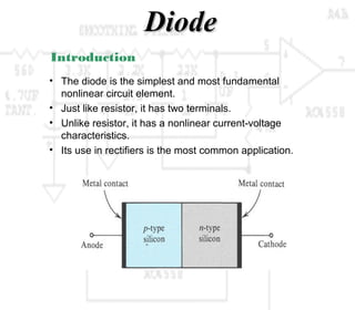
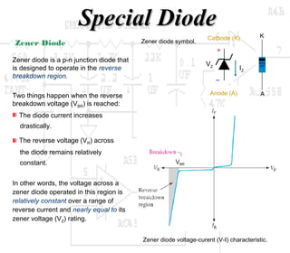
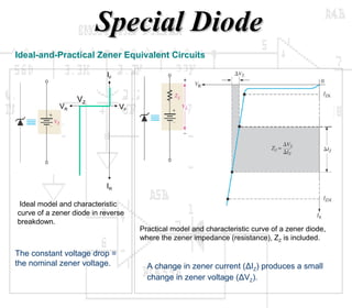
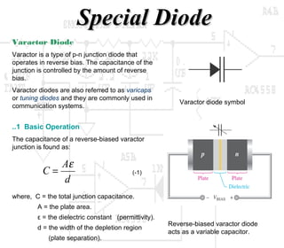
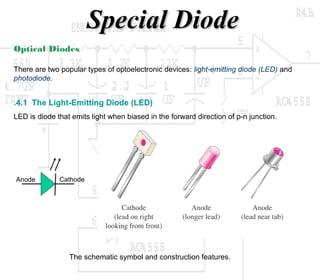
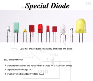
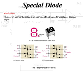
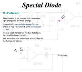
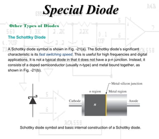
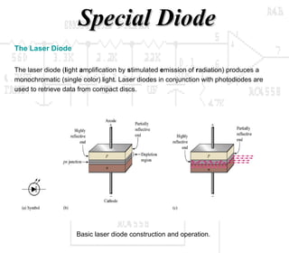
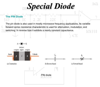
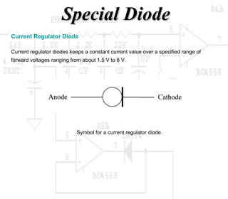
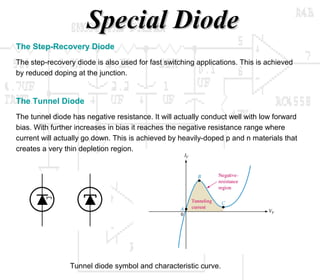
DDiiooddee && SSppeecciiaall DDiiooddee 
Made by : 
Amandeep Jangra 130080112004 
Khushboo Desai 130080112014 
Dhruvaj Suryavanshi 130080112016
Introduction 
DDiiooddee 
• The diode is the simplest and most fundamental 
nonlinear circuit element. 
• Just like resistor, it has two terminals. 
• Unlike resistor, it has a nonlinear current-voltage 
characteristics. 
• Its use in rectifiers is the most common application.
SSppeecciiaall DDiiooddee 
Zener Diode 
Zener diode is a p-n junction diode that 
is designed to operate in the reverse 
breakdown region. 
Two things happen when the reverse 
breakdown voltage (VBR) is reached: 
The diode current increases 
drastically. 
The reverse voltage (VR) across 
the diode remains relatively 
constant. 
In other words, the voltage across a 
zener diode operated in this region is 
relatively constant over a range of 
reverse current and nearly equal to its 
zener voltage (VZ) rating. 
Cathode (K) K 
+ 
− 
IZ 
VZ 
Anode (A) 
A 
Zener diode symbol. 
VBR 
Zener diode voltage-curent (V-I) characteristic.
Zener Breakdown 
SSppeecciiaall DDiiooddee 
There are two types of reverse breakdown: 
1. Avalanche breakdown. 
2. Zener breakdown. 
Avalanche breakdown is a high-field effect that occurs when the electrostatic field 
strength associated with the p-n junction is strong enough to pull electrons out of the 
valence band within the depletion region. 
Zener breakdown is a type of reverse breakdown that occurs at relatively low reverse 
voltages. The n-type and p-type materials of a zener diode are heavily doped, resulting 
in a very narrow depletion region. Therefore, the electric field existing within this region 
is intense enough to pull electrons from their valence bands and create current at a low 
reverse voltage (VR).
SSppeecciiaall DDiiooddee 
Ideal-and-Practical Zener Equivalent Circuits 
IF 
VF VR 
IR 
VZ 
Ideal model and characteristic 
curve of a zener diode in reverse 
breakdown. 
The constant voltage drop = 
the nominal zener voltage. 
Practical model and characteristic curve of a zener diode, 
where the zener impedance (resistance), ZZ is included. 
A change in zener current (ΔIZ) produces a small 
change in zener voltage (ΔVZ).
SSppeecciiaall DDiiooddee 
Varactor Diode 
Varactor is a type of p-n junction diode that 
operates in reverse bias. The capacitance of the 
junction is controlled by the amount of reverse 
bias. 
Varactor diodes are also referred to as varicaps 
or tuning diodes and they are commonly used in 
communication systems. 
..1 Basic Operation 
The capacitance of a reverse-biased varactor 
junction is found as: 
Varactor diode symbol 
Reverse-biased varactor diode 
acts as a variable capacitor. 
C = Ae 
d 
where, C = the total junction capacitance. 
A = the plate area. 
ε = the dielectric constant (permittivity). 
d = the width of the depletion region 
(plate separation). 
(-1)
Optical Diodes 
SSppeecciiaall DDiiooddee 
There are two popular types of optoelectronic devices: light-emitting diode (LED) and 
photodiode. 
.4.1 The Light-Emitting Diode (LED) 
LED is diode that emits light when biased in the forward direction of p-n junction. 
Anode Cathode 
(b) (c) 
The schematic symbol and construction features.
SSppeecciiaall DDiiooddee 
LED that are produced in an array of shapes and sizes. 
LED characteristics: 
characteristic curves are very similar to those for p-n junction diodes 
higher forward voltage (VF) 
lower reverse breakdown voltage (VBR).
SSppeecciiaall DDiiooddee 
Application 
The seven segment display is an example of LEDs use for display of decimal 
digits. 
The 7-segment LED display.
The Photodiode 
SSppeecciiaall DDiiooddee 
Photodiode is a p-n junction that can convert 
light energy into electrical energy. 
It operates in reverse bias voltage (VR), as 
shown in Fig. -18, where Iλ is the reverse light 
current. 
It has a small transparent window that allows 
light to strike the p-n junction. 
The resistance of a photodiode is calculated by 
the formula as follows: 
R VR 
R = 
l I 
Photodiode.
SSppeecciiaall DDiiooddee 
Other Types of Diodes 
The Schottky Diode 
A Schottky diode symbol is shown in Fig. -21(a). The Schottky diode’s significant 
characteristic is its fast switching speed. This is useful for high frequencies and digital 
applications. It is not a typical diode in that it does not have a p-n junction. Instead, it 
consists of a doped semiconductor (usually n-type) and metal bound together, as 
shown in Fig. -21(b). 
Schottky diode symbol and basic internal construction of a Schottky diode.
The Laser Diode 
SSppeecciiaall DDiiooddee 
The laser diode (light amplification by stimulated emission of radiation) produces a 
monochromatic (single color) light. Laser diodes in conjunction with photodiodes are 
used to retrieve data from compact discs. 
Basic laser diode construction and operation.
The PIN Diode 
SSppeecciiaall DDiiooddee 
The pin diode is also used in mostly microwave frequency applications. Its variable 
forward series resistance characteristic is used for attenuation, modulation, and 
switching. In reverse bias it exhibits a nearly constant capacitance. 
PIN diode
SSppeecciiaall DDiiooddee 
Current Regulator Diode 
Current regulator diodes keeps a constant current value over a specified range of 
forward voltages ranging from about 1.5 V to 6 V. 
Symbol for a current regulator diode.
SSppeecciiaall DDiiooddee 
The Step-Recovery Diode 
The step-recovery diode is also used for fast switching applications. This is achieved 
by reduced doping at the junction. 
The Tunnel Diode 
The tunnel diode has negative resistance. It will actually conduct well with low forward 
bias. With further increases in bias it reaches the negative resistance range where 
current will actually go down. This is achieved by heavily-doped p and n materials that 
creates a very thin depletion region. 
Tunnel diode symbol and characteristic curve.
Working principle diode and special diode

Working principle diode and special diode

  • 1.
    DDiiooddee && SSppeecciiaallDDiiooddee Made by : Amandeep Jangra 130080112004 Khushboo Desai 130080112014 Dhruvaj Suryavanshi 130080112016
  • 2.
    Introduction DDiiooddee •The diode is the simplest and most fundamental nonlinear circuit element. • Just like resistor, it has two terminals. • Unlike resistor, it has a nonlinear current-voltage characteristics. • Its use in rectifiers is the most common application.
  • 3.
    SSppeecciiaall DDiiooddee ZenerDiode Zener diode is a p-n junction diode that is designed to operate in the reverse breakdown region. Two things happen when the reverse breakdown voltage (VBR) is reached: The diode current increases drastically. The reverse voltage (VR) across the diode remains relatively constant. In other words, the voltage across a zener diode operated in this region is relatively constant over a range of reverse current and nearly equal to its zener voltage (VZ) rating. Cathode (K) K + − IZ VZ Anode (A) A Zener diode symbol. VBR Zener diode voltage-curent (V-I) characteristic.
  • 4.
    Zener Breakdown SSppeecciiaallDDiiooddee There are two types of reverse breakdown: 1. Avalanche breakdown. 2. Zener breakdown. Avalanche breakdown is a high-field effect that occurs when the electrostatic field strength associated with the p-n junction is strong enough to pull electrons out of the valence band within the depletion region. Zener breakdown is a type of reverse breakdown that occurs at relatively low reverse voltages. The n-type and p-type materials of a zener diode are heavily doped, resulting in a very narrow depletion region. Therefore, the electric field existing within this region is intense enough to pull electrons from their valence bands and create current at a low reverse voltage (VR).
  • 5.
    SSppeecciiaall DDiiooddee Ideal-and-PracticalZener Equivalent Circuits IF VF VR IR VZ Ideal model and characteristic curve of a zener diode in reverse breakdown. The constant voltage drop = the nominal zener voltage. Practical model and characteristic curve of a zener diode, where the zener impedance (resistance), ZZ is included. A change in zener current (ΔIZ) produces a small change in zener voltage (ΔVZ).
  • 6.
    SSppeecciiaall DDiiooddee VaractorDiode Varactor is a type of p-n junction diode that operates in reverse bias. The capacitance of the junction is controlled by the amount of reverse bias. Varactor diodes are also referred to as varicaps or tuning diodes and they are commonly used in communication systems. ..1 Basic Operation The capacitance of a reverse-biased varactor junction is found as: Varactor diode symbol Reverse-biased varactor diode acts as a variable capacitor. C = Ae d where, C = the total junction capacitance. A = the plate area. ε = the dielectric constant (permittivity). d = the width of the depletion region (plate separation). (-1)
  • 7.
    Optical Diodes SSppeecciiaallDDiiooddee There are two popular types of optoelectronic devices: light-emitting diode (LED) and photodiode. .4.1 The Light-Emitting Diode (LED) LED is diode that emits light when biased in the forward direction of p-n junction. Anode Cathode (b) (c) The schematic symbol and construction features.
  • 8.
    SSppeecciiaall DDiiooddee LEDthat are produced in an array of shapes and sizes. LED characteristics: characteristic curves are very similar to those for p-n junction diodes higher forward voltage (VF) lower reverse breakdown voltage (VBR).
  • 9.
    SSppeecciiaall DDiiooddee Application The seven segment display is an example of LEDs use for display of decimal digits. The 7-segment LED display.
  • 10.
    The Photodiode SSppeecciiaallDDiiooddee Photodiode is a p-n junction that can convert light energy into electrical energy. It operates in reverse bias voltage (VR), as shown in Fig. -18, where Iλ is the reverse light current. It has a small transparent window that allows light to strike the p-n junction. The resistance of a photodiode is calculated by the formula as follows: R VR R = l I Photodiode.
  • 11.
    SSppeecciiaall DDiiooddee OtherTypes of Diodes The Schottky Diode A Schottky diode symbol is shown in Fig. -21(a). The Schottky diode’s significant characteristic is its fast switching speed. This is useful for high frequencies and digital applications. It is not a typical diode in that it does not have a p-n junction. Instead, it consists of a doped semiconductor (usually n-type) and metal bound together, as shown in Fig. -21(b). Schottky diode symbol and basic internal construction of a Schottky diode.
  • 12.
    The Laser Diode SSppeecciiaall DDiiooddee The laser diode (light amplification by stimulated emission of radiation) produces a monochromatic (single color) light. Laser diodes in conjunction with photodiodes are used to retrieve data from compact discs. Basic laser diode construction and operation.
  • 13.
    The PIN Diode SSppeecciiaall DDiiooddee The pin diode is also used in mostly microwave frequency applications. Its variable forward series resistance characteristic is used for attenuation, modulation, and switching. In reverse bias it exhibits a nearly constant capacitance. PIN diode
  • 14.
    SSppeecciiaall DDiiooddee CurrentRegulator Diode Current regulator diodes keeps a constant current value over a specified range of forward voltages ranging from about 1.5 V to 6 V. Symbol for a current regulator diode.
  • 15.
    SSppeecciiaall DDiiooddee TheStep-Recovery Diode The step-recovery diode is also used for fast switching applications. This is achieved by reduced doping at the junction. The Tunnel Diode The tunnel diode has negative resistance. It will actually conduct well with low forward bias. With further increases in bias it reaches the negative resistance range where current will actually go down. This is achieved by heavily-doped p and n materials that creates a very thin depletion region. Tunnel diode symbol and characteristic curve.