Download as PPSX, PPTX
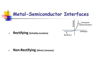
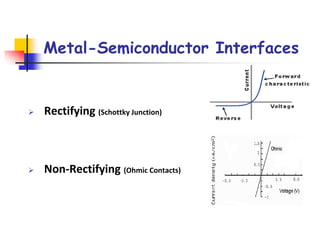


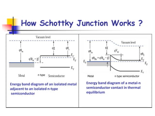


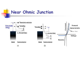
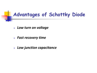

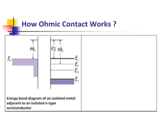
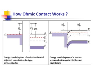
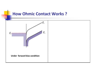


This document discusses metal-semiconductor interfaces, specifically rectifying Schottky junctions and non-rectifying ohmic contacts. It provides energy band diagrams to illustrate how Schottky junctions form a barrier under reverse bias but allow thermionic emission under forward bias, while ohmic contacts have matching work functions allowing current to flow freely. Applications of Schottky diodes mentioned include RF mixing and solar cells.


