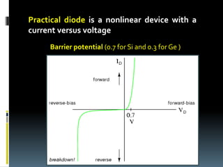
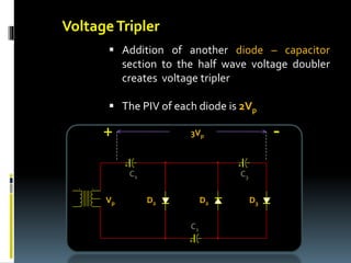
Diodes
and
Its Applications
Prepared by:
Engr. Jesus Rangcasajo
ECE 321 Instructor
jesusrangcasajo@gmail.com
Semiconductor Diode
An electronic device that results from the fusion
of P-type material and an N-type material
a. Diffusion
 movement of electrons from a region of high
concentration to lower concentration
b. At the junction, the electrons from the n-type and holes
from the p-type attract each other, combine and cancel their
net charges
Formation of the Depletion Region
C A
Junction
c. Due to the cancellation of electrons and
holes at the junction, the junction will have no
more carriers so it is called a depleted region
or depletion region.
Depletion region
C A
Practical diode is a nonlinear device with a
current versus voltage
Barrier potential (0.7 for Si and 0.3 for Ge )
To simplify the analysis of diode circuits,
Diodes are assumed to be Ideal.
Short circuit when forward biased
Open circuit when reverse biased
a.Forward Biased
 P-type is more positive than the N-type
 A condition that allows current to flow through
the pn junction
 The pn junction narrows
Biasing the PN Junction
Forward Biases Conditions
1. Anode must be positive with respect to
cathode
2. The potential difference (Vd) should be
greater than the diode threshold voltage
(Vth)
ThresholdVoltage
- Required voltage across the junction of the
diode before forward current can flow
significantly
b. Reverse Biased
 P-type is more negative than the N-type
 A condition that prevents current to flow through the pn
junction
 The pn junction widens
Reverse Biased Conditions
1. Cathode must be positive with respect to anode
2. The potential difference should not be greater than
the diode’s breakdown voltage
BreakdownVoltage:
- Maximum voltage the junction diode can handle when
reverse biased
- Also called Peak ReverseVoltage & Peak Inverse
Voltage
Note:
Silicon has relatively higher breakdown voltage than
Germanium
I. Applications
1. Diode Rectifier
 Type of diode that converts alternating
current into unidirectional current (DC)
 Typically seen in power supplies
Rectifier
Regulator
Filter
AC
Power Supply
Half – Wave Rectifier
 A rectifier circuit with a single diode that
conducts current during positive or
negative half cycles of input AC signal at a
rate determined by the input frequency.
Input
Output
Conversion factor = 40.6%
Freqoutput = Freqinput
Full – Wave Rectifier
 A rectifier circuit that conducts current
during positive and negative half cycles of
input AC signal.
Input
Output
Center –Tapped
Input
Output
Conversion factor = 81.2%
Freqoutput = 2 x Freqinput
BridgeType
Half – Wave Center –tapped BridgeType
Vrms Vpk / 2 Vpk / √2 Vpk / √2
Vave Vpk / ∏ 2Vpk / ∏ 2Vpk / ∏
Irms Ipk / 2 Ipk / √2 Ipk / √2
Iave Ipk / ∏ 2Ipk / ∏ 2Ipk / ∏
PIV Vpk 2Vpk Vpk
Comparison of Rectifiers
Filter
 Smoothens the output waveform
Ripple Factor of a Rectifier
 Ratio of the rms value of the AC
component of the signal to the average
value of the signal
Vr(rms) = 0.385 (Vpeak for Half wave Rectifier)
Vr(rms) = 0.308 (Vpeak for Full Rectifier)
𝑟 =
𝑉𝑟(𝑟𝑚𝑠)
𝑉𝑑𝑐
𝑉𝑟(𝑟𝑚𝑠)=
1
2
( 𝑉𝑟𝑚𝑠 2 − (𝑉𝑑𝑐)2)
Voltage Regulation
 Means maintaining the output voltage at
any load
 The type of diode used for regulation is
Zener diode
ID
Avalanche
region
Iz min
Iz max
Zener
Regulation
Voltage Regulation
Current Regulation
𝑉𝑅 =
𝑉𝑛𝑜𝑙𝑜𝑎𝑑 − 𝑉𝑓𝑢𝑙𝑙𝑙𝑜𝑎𝑑
𝑉𝑓𝑢𝑙𝑙𝑙𝑜𝑎𝑑
𝑥 100%
C𝑅 =
𝐼𝑛𝑜𝑙𝑜𝑎𝑑 −𝐼𝑓𝑢𝑙𝑙𝑙𝑜𝑎𝑑
𝐼𝑓𝑢𝑙𝑙𝑙𝑜𝑎𝑑
𝑥 100%
2. Clippers
 Electronic circuits that have the
ability to clip – off a portion of the
input signal without distorting the
remaining part of the alternating
waveform
 Other names are limiters,
amplitude selectors and slicers
Input
Output
Example of Clipper Circuit
Input
Output
DC signal
Example of Clipper Circuit
Analysis of Clippers - Short Cut Method
1. Determine the output waveform without the
effect of the diode by
a. shorting the diode for series limiter
b. opening the diode for parallel limiter.
2. Determine the Clipping Line
a. For Series Limiter, the clipping line is at the
abscissa.
b. For Parallel Limiter, the clipping line is the
output reflection of the voltage source; if there
is no voltage source present, the clipping line is
at the abscissa.
Analysis of Clippers - Short Cut Method
3. Inspect the position of the diode
a. For series limiters, if the arrowhead of the diode is
i. pointing to the right, the output waveform is above
the clipping line.
ii. Pointing to the left, the output waveform is below
the clipping line
b. For parallel limiters, if the arrowhead of the diode is
i. pointing upward, the output waveform is above the
clipping line.
ii. Pointing downward, the output waveform is below
the clipping line.
Analysis of Clippers - Short Cut Method
4. For Double Diode Clippers, same procedure for 1 and 2.
The resulting waveforem is between the 2 clipping
lines.
3. Clampers
 Circuits that shift the waveform of
the input signal either all above or
below the reference voltage
 Add or restore a DC level to an
electrical signal
 Also known as DC restorer
 Clamping circuit is often used in
television receivers as dc restorer.
Incoming composite video signal is
normally processed through
capacitively coupled amplifiers that
eliminate the dc component losing
the reference levels which must be
restored using clamping circuits
before applying to the picture tube.
Example of Clamper Circuit
Input
Output
Vpk
2Vpk
Positive Clamper
Analysis of Clampers - Short Cut Method
1. Determine the Clamping Line as given by the output
reflection of the voltage source. If there is no voltage
source present, the clamping line is at the abscissa.
Note: There should be no part of the waveform to be
either above or below the clamping line.
2. Determine where the arrowhead of the diode is
pointing
a. upward, the waveform is above the clamping line.
b. downward, the waveform is below the clamping
line.
4. Voltage Multiplier
 Circuit which produces a greater DC output
voltage than AC input voltage to the
rectifiers
 Uses clamping action to increase peak
rectified voltages without the necessity of
increasing the input’s transformers voltage
rating
 Used in high – voltage, low current
applications such asTV receivers
Voltage Doubler
 A voltage multiplier with a multiplication
factor of 2
C1
C2D1
D2
Vp Vo
At the first negative half cylcle
D1 = forward bias
D2 = reverse bias
VC1 =Vp
VC2 = 2Vp
At the first positivehalf cylcle
D1 = reverse bias
D2 = forward bias
VC1 =Vp
Vo =VC2 = 2Vp
VoltageTripler
 Addition of another diode – capacitor
section to the half wave voltage doubler
creates voltage tripler
 The PIV of each diode is 2Vp
3Vp
Vp
C1
D2 D2 D3
C3
C2
+ -
Voltage Quadrupler
 The addition of still another diode –
capacitor section in a voltage tripler circuit
 The PIV of each diode is 2Vp
C1 C3
C2 C4
Vp D1 D2 D3 D4
4Vp
+ -
II. Special Purpose Diodes
1. Zener Diode
Symbol
 Diode designed to operate in the reverse
breakdown region
a. Zener breakdown
 When the breakdown voltage is below 5V
b. Avalanche breakdown
 When the breakdown voltage is above 5V
2. Zener Diode
 Typical breakdown voltages of 1.8V
to 200V with specified tolerances
from 1% to 20%
 With very stable voltage drop
 Useful as voltage regulator
2. Point Contact Diode
 Semiconductor diode having fine
wire whose point is permanent
contact with the surface of a wafer
of a semiconductor material such as
silicon, germanium or gallium
arsenide
 The fine wire is called cat - whisker
 For signal mixing and detection
2. Point Contact Diode
3. Schottky Diode
Symbol
 Also known as Surface Barrier Diode
 Also known as Hot - Carrier Diode
 This type of diode has no depletion layer
which eliminates the stored charges in the
junction
 A rectifying metal semiconductor junction
such as gold, silver and platinum
3. Schottky Diode
Construction of Schottky Diode
cathode anode
Metal Silicon Junction
 Typical forward voltage drop is typically
around 0.25V to 0.3V
 Can rectify frequencies up to 300 MHz
 ESBAR (Epitaxial Schottky Barrier)
4. Varactor (varicap)
 Voltage-variable capacitor
 When this diode is reverse bias, the width
of the depletion layer increases with the
reverse voltage
 Used for electronic tuning, harmonic
generator and parametric amplifier
Symbol
where
f = frequency
Rs = series resistance
Ct = total diode
capacitance
5. Tunnel Diode
Symbol
5. Tunnel Diode
 Also known as Esaki diode
 Type of diode that exhibits the
phenomenon known as negative
resistance
 Negative resistance implies that an
increase in forward voltage produces a
decrease in forward current for a certain
part
 Utilizes a heavily doped material and
therefore have so many electrons
 Has a very thin depletion layer
 The extremely narrow depletion region
emits electrons to “tunnel” through the pn
junction at very low forward bias voltage
 Used for oscillators and amplifiers
6. Backward Diode
Symbol
6. Backward Diode
 Conducts better in the reverse (-0.1V) than
in the forward (+0.7V) direction
 Designed such that its high current flow
takes place when the junction is reverse
bias
7. PIN Diode
 Positive – intrinsic Negative Diode
 The intrinsic material between the P and N
layer offers impedance at microwave
frequencies being controlled by low
frequency signals
 Used in microwave switches
8. Light Emitting Diode (LED)
Symbol
8. Light Emitting Diode (LED)
 In a forward biased LED, free electrons
cross the junction and fall into holes. As
these electrons fall from higher to a lower
energy level, they radiate energy which
goes off in the form of heat. But in an LED,
the energy is being radiated as light.
 Commonly used Gallium Arsenide,
Gallium Arsenide Phosphide, and Gallium
Phosphide
 GaAs LEDs emit infrared (IR) radiation
which is non visible, GaAsP produces
either red or yellow visible light and GaP
emits red or green visible light
 Red is the most common color of LEDs
 Electroluminescence is the process
involved when large surface area on one
layer of one semiconductive material
permits the photons to be emitted as
visible light
Metal contact Metal contact
P N
EmittedVisible Light
(–)
(+)
 Irradiance is the power per unit area at a
given distance from an LED source
expressed in mW/cm2.
 Typical voltage drop: 1.5V to 2.5V for
currents between 10mA and 50mA
 NominalVoltage drop: 2V
 Reverse Breakdown: 3V – 10V
9. LASER Diode
 The term LASER stands for Light
Amplification by Stimulated Emission of
Radiation
 LASER light is monochromatic meaning it
consists of a single color and not a mixture
of colors
 LASER light is also a coherent light
meaning a single wavelength
9. LASER Diode
LASER Light (coherent and monochromatic)
 LASER diode pn junction is formed by two
layers of doped gallium arsenide
 It is forward biased
 LASER diodes and photodiodes are used in
the pick – up system of compact disk (CD)
layers. Audio information is digitally
recorded in stereo on the surface of a
compact disk in the microscopic “pits and
flats”
10. Photodiode
Symbol
10. Photodiode
 Operated in reverse bias condition
 Is one that is optimized for its sensitivity to
light
 A window let light to pass through the
package of the junction. The incoming light
produces free electrons and holes
producing larger reverse current.
 Dark current is the reverse current flowing
through the photodiode when there is no
incident light.
Review Questions
Diodes and Applications
Review Questions
Diodes and Applications
1. The arrow in the schematic symbol for a diode
points which way
a. towards the cathode
b. in the direction of the current flow
c. towards the anode
d. towards magnetic north
a. towards the cathode
Review Questions
Diodes and Applications
2. The anode of a semiconductor diode indicates
a __________ charge during conduction
a. positive
b. either, depending on the design
c. neutral
d. negative
a. positive
Review Questions
Diodes and Applications
3. A point in the characteristic curve of a diode
where the current suddenly rises
a. peak voltage
b. knee voltage
c. valley voltage
d. trigger voltage
b. knee voltage
Review Questions
Diodes and Applications
4. The small value of direct current that flows
when a semiconductor device has a reverse
bias
a. surge current
b. bias current
c. reverse current
d. current limit
c. reverse current
Review Questions
Diodes and Applications
5. In order to simplify a circuit, in analysis and
computation, the diode is normally assumed
as __________.
a. zero
b. ideal
c. imaginary
d. infinite
b. ideal
Review Questions
Diodes and Applications
6.An external voltage applied to a junction
reduces its barrier and aid current to flow
through the junction
a. reverse bias
b. external bias
c. junction bias
d. forward bias
d. forward bias
Review Questions
Diodes and Applications
7. How does an ohmmeter behave if its positive
lead is connected to the cathode of a diode
while negative to anode?
a. has infinite high resistance
b. has unstable resistance
c. has very low resistance
d. has decreasing resistance
a. has infinite high resistance
Review Questions
Diodes and Applications
8. It is the maximum permissible reverse voltage
for the diode
a. peak reverse voltage
b. barrier voltage
c. maximum voltage
d. tolerable voltage
a. peak reverse voltage
Review Questions
Diodes and Applications
9. Circuit that is used to eliminate or portions of
the input waveform above or below a
specified level
a. clamper
b. clipper
c. DC restorer
d. multiplier
b. clipper
Review Questions
Diodes and Applications
10. Which is not an application of clipper?
a. circuit transient protection
b. changing the shape of the waveform
c. detection
d. oscillation
d. oscillation
Review Questions
Diodes and Applications
11. What is another name for clamper?
a. slicer
b. limiter
c. clipper
d. DC restorer
d. DC restorer
Review Questions
Diodes and Applications
12. Circuit that is used to produce a DC output
voltage that is some integral multiple of the
peak of the AC input voltage
a. integrator
b. restorer
c. differentiator
d. multiplier
d. multiplier
Review Questions
Diodes and Applications
13. What is the process by which AC is converted
to pulsating DC?
a. charging
b. rectification
c. filtering
d. clipping
b. rectification
Review Questions
Diodes and Applications
14. _________ is the output of a half – wave
rectifier
a. half – wave rectified signal
b. square wave signal
c. 100%AC signal
d. sinusoidal signal
a. half – wave rectified signal
Review Questions
Diodes and Applications
15. How many diodes will you use to have a
basic half – wave rectifier?
a. three
b. four
c. two
d. one
d. one
Review Questions
Diodes and Applications
16. The four basic circuit blocks that make up a
power supply are
a. transformer, clipper, filter, regulator
b. rectifier, clamper, filter, regulator
c. transformer, rectifier, inverter, regulator
d. transformer, rectifier, filter, regulator
Review Questions
Diodes and Applications
17. What is the ideal voltage regulation of a
power supply?
a. 0%
b. 50%
c. 100%
d. 1%
a. 0%
Review Questions
Diodes and Applications
18. It is a type of transformer whose secondary
voltage is equal to the primary voltage and
used to isolate electrically the power supply
from the AC power line thus protecting the
power supply and the technician who is
working on it
a. autotransformer
b. step – down transformer
c. step – up transformer
d. isolation transformer
Review Questions
Diodes and Applications
19. Find the direct current voltage from a full –
wave rectifier with 120V peak rectified
voltage
a. 60V
b. 7.639V
c. 76.39V
d. 6.0V
c. 76.39V
Review Questions
Diodes and Applications
20. What is the maximum efficiency of a half –
wave rectifier?
a. 50%
b. 40.6%
c. 81.2%
d. 100%
b. 40.6%
Review Questions
Diodes and Applications
21. A half – wave rectifier circuit utilizing one
half of an AC input cycle have a ripple
frequency in its output equivalent to
a. 60 cps
b. 120 cps
c. 110 cps
d. 240 cps
a. 60 cps
Review Questions
Diodes and Applications
22. Find the ripple factor (kr) of sinusoidal signal
with peak ripple of 4V on an average of 30
a. 0.094
b. 0.013
c. 0.130
d. 0.940
a. 0.094
Review Questions
Diodes and Applications
23. It the remaining variation in the output of a
power supply filter
a. residual voltage
b. ripple
c. offset voltage
d. persistent voltage
b. ripple
Review Questions
Diodes and Applications
24. A DC voltage supply is measured at 50V and
drops to 45V when the load is connected.
What is the value of “voltage regulation”?
a. 5%
b. 50%
c. 60%
d. 11.11%
d. 11.11%
Review Questions
Diodes and Applications
25. How much voltage regulation does
commercial power supply have?
a. 10%
b. 10% and above
c. 15% and above
d. within 1%
d. within 1%
Review Questions
Diodes and Applications
26. What is the voltage regulation when the full
load voltage is the same as no – load voltage
assuming a perfect voltage source?
a. 100%
b. 0%
c. 1%
d. 10%
b. 0%
Review Questions
Diodes and Applications
27. _________ is a type of linear voltage used in
application where the load on the
unregulated voltage source must be kept
constant
a. a series regulator
b. a constant current source
c. a shunt current source
d. a shunt regulator
Review Questions
Diodes and Applications
28. __________ is a type of linear regulator used
in applications requiring efficient utilization
of the primary power source
a. a series regulator
b. a shunt regulator
c. a constant current source
d. a shunt current source
a. a series regulator
Review Questions
Diodes and Applications
29. It is the sudden current and voltage spike
that has a small duration
a. transient
b.Vrms
c. peak voltage
d.VDC
a. transient
Review Questions
Diodes and Applications
30. It is the component that is used to provide a
discharge path for the capacitor in a voltage
multiplier if the load opens
a. discharging path
b. tuned circuit
c. inductive path
d. bleeder resistor
d. bleeder resistor
Review Questions
Diodes and Applications
31. How do you determine if a diode is
defective?
a. diode resistance is very low or very high on either
direction
b. high current
c. very low current
d. high voltage
a. diode resistance is very low or
very high on either direction
Review Questions
Diodes and Applications
32. The term used to describe sudden reverse
conduction of an electronic component
cause by excess reverse voltage across the
device
a. cut – off
b. saturation
c. avalanche
d. reversion
c. avalanche
Review Questions
Diodes and Applications
33. How do zener diodes widely used?
a. current limiter
b. variable resistors
c. voltage regulators
d. power collectors
c. voltage regulators
Review Questions
Diodes and Applications
34. __________ is a PN junction semiconductor
device that emits non coherent optical
radiation when biased in the forward
direction, as a result of a recombination
effect.
a. LASER
b. JUGPET
c. LED
d. optical cavity
c. LED
Review Questions
Diodes and Applications
35. What type of bias is required for an LED to
produce luminescence?
a. reverse bias
b. zero bias
c. forward bias
d. inductive bias
c. forward bias
Review Questions
Diodes and Applications
36. What special type of diode is capable of both
amplification and oscillation?
a. point contact diode
b. junction diode
c. zener diode
d. tunnel diode
d. tunnel diode
Review Questions
Diodes and Applications
37. Which is the principal characteristic of a
tunnel diode?
a. a very high PIV
b. a high forward current rating
c. a high forward resistance
d. a negative resistance region
Review Questions
Diodes and Applications
38. A high – speed diode with very small junction
capacitance
a. silicon diode
b. schottky
c. germanium diode
d. tunnel
b. schottky
Review Questions
Diodes and Applications
39. Which is the principal characteristic of a
varactor diode?
a. it has a very high PIV
b. it has a negative region
c. its internal capacitance varies with the applied
voltage
d. it has a constant voltage under conditions of
varying current
c. its internal capacitance varies with
the applied voltage
Review Questions
Diodes and Applications
40. It is the factor by which the capacitance of
the varactor changes from one special value
of reverse voltage to another
a. capacitance factor
b. variance factor
c. capacitance ratio
d. reactance factor
c. capacitance ratio
Review Questions
Diodes and Applications
41. A varactor diode with a high capacitance
ratio can be used in
a. tuning fork
b. coarse tuning
c. phase tuning
d. fine tuning
b. coarse tuning
Review Questions
Diodes and Applications
42. It is a kind of a tuning circuit that is used to
vary the value of the resonant frequency
over a wide range of frequencies
a. resonant circuit
b. band wide circuit
c. fine tuning circuit
d. coarse tuning circuit
Review Questions
Diodes and Applications
43. It is a diode whose central material is made
up of intrinsic silicon sandwiched by p and n
type materials
a. PIN
b. zener
c. schottky
d. tunnel
a. PIN
Review Questions
Diodes and Applications
44. Type of diode that is made of metal whisker
touching a very small semiconductor die
a. a junction diode
b. varactor diode
c. point contact diode
d. zener diode
c. point contact diode
Review Questions
Diodes and Applications
45. It is a circuit that uses two diodes to provide
DC output voltage equal to twice the AC
voltage
a. voltage doubler
b. voltage regulator
c. voltage multiplier
d. all of these
a. voltage doubler
Review Questions
Diodes and Applications
46. Without a DC source, a clipper acts like a
a. rectifier
b. clamper
c. demodulator
d. chopper
a. rectifier
Review Questions
Diodes and Applications
47. The main job of a voltage regulator is to
provide a nearly __________ output voltage
a. sinusoidal
b. constant
c. smooth
d. fluctuating
b. constant
Review Questions
Diodes and Applications
48. The average value of a half – wave rectified
voltage with a peak value of 200V is
a. 63.7V
b. 127.3V
c. 141V
d. 0V
a. 63.7V
Review Questions
Diodes and Applications
49. When the peak output voltage is 100V the
PIV for each diode in the center – tapped full
– wave rectifier is (neglecting the diode drop)
a. 100V
b. 200V
c. 141V
d. 50V
b. 200V
Review Questions
Diodes and Applications
50. When the rms output voltage of a full –wave
bridge rectifier is 20V, the peak inverse
voltage across the diodes is (neglecting the
diode drop)
a. 20V
b. 40V
c. 28.3V
d. 56.6V
c. 28.3V
Review Questions
Diodes and Applications
51. If the input voltage to a voltage tripler has an
rms value of 12V, the DC output voltage is
approximately
a. 36V
b. 50.9V
c. 33.9V
d. 32.4V
b. 50.9V
Review Questions
Diodes and Applications
52. A transformer giving secondary voltage of 9V
rms is used in a half – wave rectifier circuit.
The peak inverse voltage across the diodes is
a. 9V
b. 13V
c. 18V
d. 26V
b. 13V
Review Questions
Diodes and Applications
53. A certain power supply filter produces an
output with a ripple of 100mV peak – to –
peak and a DC value of 20V. The ripple factor
is
a. 0.05
b. 0.005
c. 0.00005
d. 0.02
b. 0.005
Review Questions
Diodes and Applications
54. The ripple of a filter output voltage with the
following output signal measurement of
VDC = 30V andVrms = 1.5V is
a. 9.5%
b. 95%
c. 5%
d. 50%
c. 5%
Review Questions
Diodes and Applications
55. Find the voltage regulation giving a DC
voltage of 67V without load and with full
load current drawn the output voltage drops
to 42V.
a. 59.5%
b. 62.7%
c. 15.9%
d. 32.5%
a. 59.5%
Thank
you

Diodes and Its Application

  • 1.
    Diodes and Its Applications Prepared by: Engr.Jesus Rangcasajo ECE 321 Instructor jesusrangcasajo@gmail.com
  • 2.
    Semiconductor Diode An electronicdevice that results from the fusion of P-type material and an N-type material
  • 3.
    a. Diffusion  movementof electrons from a region of high concentration to lower concentration b. At the junction, the electrons from the n-type and holes from the p-type attract each other, combine and cancel their net charges Formation of the Depletion Region C A Junction
  • 4.
    c. Due tothe cancellation of electrons and holes at the junction, the junction will have no more carriers so it is called a depleted region or depletion region. Depletion region C A
  • 5.
    Practical diode isa nonlinear device with a current versus voltage Barrier potential (0.7 for Si and 0.3 for Ge )
  • 6.
    To simplify theanalysis of diode circuits, Diodes are assumed to be Ideal. Short circuit when forward biased Open circuit when reverse biased
  • 7.
    a.Forward Biased  P-typeis more positive than the N-type  A condition that allows current to flow through the pn junction  The pn junction narrows Biasing the PN Junction
  • 8.
    Forward Biases Conditions 1.Anode must be positive with respect to cathode 2. The potential difference (Vd) should be greater than the diode threshold voltage (Vth) ThresholdVoltage - Required voltage across the junction of the diode before forward current can flow significantly
  • 9.
    b. Reverse Biased P-type is more negative than the N-type  A condition that prevents current to flow through the pn junction  The pn junction widens
  • 10.
    Reverse Biased Conditions 1.Cathode must be positive with respect to anode 2. The potential difference should not be greater than the diode’s breakdown voltage BreakdownVoltage: - Maximum voltage the junction diode can handle when reverse biased - Also called Peak ReverseVoltage & Peak Inverse Voltage Note: Silicon has relatively higher breakdown voltage than Germanium
  • 11.
    I. Applications 1. DiodeRectifier  Type of diode that converts alternating current into unidirectional current (DC)  Typically seen in power supplies Rectifier Regulator Filter AC Power Supply
  • 12.
    Half – WaveRectifier  A rectifier circuit with a single diode that conducts current during positive or negative half cycles of input AC signal at a rate determined by the input frequency. Input Output Conversion factor = 40.6% Freqoutput = Freqinput
  • 13.
    Full – WaveRectifier  A rectifier circuit that conducts current during positive and negative half cycles of input AC signal. Input Output Center –Tapped
  • 14.
    Input Output Conversion factor =81.2% Freqoutput = 2 x Freqinput BridgeType
  • 15.
    Half – WaveCenter –tapped BridgeType Vrms Vpk / 2 Vpk / √2 Vpk / √2 Vave Vpk / ∏ 2Vpk / ∏ 2Vpk / ∏ Irms Ipk / 2 Ipk / √2 Ipk / √2 Iave Ipk / ∏ 2Ipk / ∏ 2Ipk / ∏ PIV Vpk 2Vpk Vpk Comparison of Rectifiers
  • 16.
    Filter  Smoothens theoutput waveform
  • 17.
    Ripple Factor ofa Rectifier  Ratio of the rms value of the AC component of the signal to the average value of the signal Vr(rms) = 0.385 (Vpeak for Half wave Rectifier) Vr(rms) = 0.308 (Vpeak for Full Rectifier) 𝑟 = 𝑉𝑟(𝑟𝑚𝑠) 𝑉𝑑𝑐 𝑉𝑟(𝑟𝑚𝑠)= 1 2 ( 𝑉𝑟𝑚𝑠 2 − (𝑉𝑑𝑐)2)
  • 18.
    Voltage Regulation  Meansmaintaining the output voltage at any load  The type of diode used for regulation is Zener diode ID Avalanche region Iz min Iz max Zener Regulation
  • 19.
    Voltage Regulation Current Regulation 𝑉𝑅= 𝑉𝑛𝑜𝑙𝑜𝑎𝑑 − 𝑉𝑓𝑢𝑙𝑙𝑙𝑜𝑎𝑑 𝑉𝑓𝑢𝑙𝑙𝑙𝑜𝑎𝑑 𝑥 100% C𝑅 = 𝐼𝑛𝑜𝑙𝑜𝑎𝑑 −𝐼𝑓𝑢𝑙𝑙𝑙𝑜𝑎𝑑 𝐼𝑓𝑢𝑙𝑙𝑙𝑜𝑎𝑑 𝑥 100%
  • 20.
    2. Clippers  Electroniccircuits that have the ability to clip – off a portion of the input signal without distorting the remaining part of the alternating waveform  Other names are limiters, amplitude selectors and slicers
  • 21.
  • 22.
  • 23.
    Analysis of Clippers- Short Cut Method 1. Determine the output waveform without the effect of the diode by a. shorting the diode for series limiter b. opening the diode for parallel limiter. 2. Determine the Clipping Line a. For Series Limiter, the clipping line is at the abscissa. b. For Parallel Limiter, the clipping line is the output reflection of the voltage source; if there is no voltage source present, the clipping line is at the abscissa.
  • 24.
    Analysis of Clippers- Short Cut Method 3. Inspect the position of the diode a. For series limiters, if the arrowhead of the diode is i. pointing to the right, the output waveform is above the clipping line. ii. Pointing to the left, the output waveform is below the clipping line b. For parallel limiters, if the arrowhead of the diode is i. pointing upward, the output waveform is above the clipping line. ii. Pointing downward, the output waveform is below the clipping line.
  • 25.
    Analysis of Clippers- Short Cut Method 4. For Double Diode Clippers, same procedure for 1 and 2. The resulting waveforem is between the 2 clipping lines.
  • 26.
    3. Clampers  Circuitsthat shift the waveform of the input signal either all above or below the reference voltage  Add or restore a DC level to an electrical signal  Also known as DC restorer
  • 27.
     Clamping circuitis often used in television receivers as dc restorer. Incoming composite video signal is normally processed through capacitively coupled amplifiers that eliminate the dc component losing the reference levels which must be restored using clamping circuits before applying to the picture tube.
  • 28.
    Example of ClamperCircuit Input Output Vpk 2Vpk Positive Clamper
  • 29.
    Analysis of Clampers- Short Cut Method 1. Determine the Clamping Line as given by the output reflection of the voltage source. If there is no voltage source present, the clamping line is at the abscissa. Note: There should be no part of the waveform to be either above or below the clamping line. 2. Determine where the arrowhead of the diode is pointing a. upward, the waveform is above the clamping line. b. downward, the waveform is below the clamping line.
  • 30.
    4. Voltage Multiplier Circuit which produces a greater DC output voltage than AC input voltage to the rectifiers  Uses clamping action to increase peak rectified voltages without the necessity of increasing the input’s transformers voltage rating  Used in high – voltage, low current applications such asTV receivers
  • 31.
    Voltage Doubler  Avoltage multiplier with a multiplication factor of 2 C1 C2D1 D2 Vp Vo At the first negative half cylcle D1 = forward bias D2 = reverse bias VC1 =Vp VC2 = 2Vp At the first positivehalf cylcle D1 = reverse bias D2 = forward bias VC1 =Vp Vo =VC2 = 2Vp
  • 32.
    VoltageTripler  Addition ofanother diode – capacitor section to the half wave voltage doubler creates voltage tripler  The PIV of each diode is 2Vp 3Vp Vp C1 D2 D2 D3 C3 C2 + -
  • 33.
    Voltage Quadrupler  Theaddition of still another diode – capacitor section in a voltage tripler circuit  The PIV of each diode is 2Vp C1 C3 C2 C4 Vp D1 D2 D3 D4 4Vp + -
  • 34.
    II. Special PurposeDiodes 1. Zener Diode Symbol
  • 35.
     Diode designedto operate in the reverse breakdown region a. Zener breakdown  When the breakdown voltage is below 5V b. Avalanche breakdown  When the breakdown voltage is above 5V 2. Zener Diode
  • 36.
     Typical breakdownvoltages of 1.8V to 200V with specified tolerances from 1% to 20%  With very stable voltage drop  Useful as voltage regulator
  • 37.
  • 38.
     Semiconductor diodehaving fine wire whose point is permanent contact with the surface of a wafer of a semiconductor material such as silicon, germanium or gallium arsenide  The fine wire is called cat - whisker  For signal mixing and detection 2. Point Contact Diode
  • 39.
  • 40.
     Also knownas Surface Barrier Diode  Also known as Hot - Carrier Diode  This type of diode has no depletion layer which eliminates the stored charges in the junction  A rectifying metal semiconductor junction such as gold, silver and platinum 3. Schottky Diode
  • 41.
    Construction of SchottkyDiode cathode anode Metal Silicon Junction  Typical forward voltage drop is typically around 0.25V to 0.3V  Can rectify frequencies up to 300 MHz  ESBAR (Epitaxial Schottky Barrier)
  • 42.
  • 43.
     Voltage-variable capacitor When this diode is reverse bias, the width of the depletion layer increases with the reverse voltage  Used for electronic tuning, harmonic generator and parametric amplifier Symbol where f = frequency Rs = series resistance Ct = total diode capacitance
  • 44.
  • 45.
    5. Tunnel Diode Also known as Esaki diode  Type of diode that exhibits the phenomenon known as negative resistance
  • 46.
     Negative resistanceimplies that an increase in forward voltage produces a decrease in forward current for a certain part  Utilizes a heavily doped material and therefore have so many electrons  Has a very thin depletion layer  The extremely narrow depletion region emits electrons to “tunnel” through the pn junction at very low forward bias voltage  Used for oscillators and amplifiers
  • 47.
  • 48.
    6. Backward Diode Conducts better in the reverse (-0.1V) than in the forward (+0.7V) direction  Designed such that its high current flow takes place when the junction is reverse bias
  • 49.
    7. PIN Diode Positive – intrinsic Negative Diode  The intrinsic material between the P and N layer offers impedance at microwave frequencies being controlled by low frequency signals  Used in microwave switches
  • 50.
    8. Light EmittingDiode (LED) Symbol
  • 51.
    8. Light EmittingDiode (LED)  In a forward biased LED, free electrons cross the junction and fall into holes. As these electrons fall from higher to a lower energy level, they radiate energy which goes off in the form of heat. But in an LED, the energy is being radiated as light.
  • 52.
     Commonly usedGallium Arsenide, Gallium Arsenide Phosphide, and Gallium Phosphide  GaAs LEDs emit infrared (IR) radiation which is non visible, GaAsP produces either red or yellow visible light and GaP emits red or green visible light  Red is the most common color of LEDs
  • 53.
     Electroluminescence isthe process involved when large surface area on one layer of one semiconductive material permits the photons to be emitted as visible light Metal contact Metal contact P N EmittedVisible Light (–) (+)
  • 54.
     Irradiance isthe power per unit area at a given distance from an LED source expressed in mW/cm2.  Typical voltage drop: 1.5V to 2.5V for currents between 10mA and 50mA  NominalVoltage drop: 2V  Reverse Breakdown: 3V – 10V
  • 55.
  • 56.
     The termLASER stands for Light Amplification by Stimulated Emission of Radiation  LASER light is monochromatic meaning it consists of a single color and not a mixture of colors  LASER light is also a coherent light meaning a single wavelength 9. LASER Diode
  • 57.
    LASER Light (coherentand monochromatic)
  • 58.
     LASER diodepn junction is formed by two layers of doped gallium arsenide  It is forward biased  LASER diodes and photodiodes are used in the pick – up system of compact disk (CD) layers. Audio information is digitally recorded in stereo on the surface of a compact disk in the microscopic “pits and flats”
  • 59.
  • 60.
    10. Photodiode  Operatedin reverse bias condition  Is one that is optimized for its sensitivity to light  A window let light to pass through the package of the junction. The incoming light produces free electrons and holes producing larger reverse current.  Dark current is the reverse current flowing through the photodiode when there is no incident light.
  • 61.
  • 62.
    Review Questions Diodes andApplications 1. The arrow in the schematic symbol for a diode points which way a. towards the cathode b. in the direction of the current flow c. towards the anode d. towards magnetic north a. towards the cathode
  • 63.
    Review Questions Diodes andApplications 2. The anode of a semiconductor diode indicates a __________ charge during conduction a. positive b. either, depending on the design c. neutral d. negative a. positive
  • 64.
    Review Questions Diodes andApplications 3. A point in the characteristic curve of a diode where the current suddenly rises a. peak voltage b. knee voltage c. valley voltage d. trigger voltage b. knee voltage
  • 65.
    Review Questions Diodes andApplications 4. The small value of direct current that flows when a semiconductor device has a reverse bias a. surge current b. bias current c. reverse current d. current limit c. reverse current
  • 66.
    Review Questions Diodes andApplications 5. In order to simplify a circuit, in analysis and computation, the diode is normally assumed as __________. a. zero b. ideal c. imaginary d. infinite b. ideal
  • 67.
    Review Questions Diodes andApplications 6.An external voltage applied to a junction reduces its barrier and aid current to flow through the junction a. reverse bias b. external bias c. junction bias d. forward bias d. forward bias
  • 68.
    Review Questions Diodes andApplications 7. How does an ohmmeter behave if its positive lead is connected to the cathode of a diode while negative to anode? a. has infinite high resistance b. has unstable resistance c. has very low resistance d. has decreasing resistance a. has infinite high resistance
  • 69.
    Review Questions Diodes andApplications 8. It is the maximum permissible reverse voltage for the diode a. peak reverse voltage b. barrier voltage c. maximum voltage d. tolerable voltage a. peak reverse voltage
  • 70.
    Review Questions Diodes andApplications 9. Circuit that is used to eliminate or portions of the input waveform above or below a specified level a. clamper b. clipper c. DC restorer d. multiplier b. clipper
  • 71.
    Review Questions Diodes andApplications 10. Which is not an application of clipper? a. circuit transient protection b. changing the shape of the waveform c. detection d. oscillation d. oscillation
  • 72.
    Review Questions Diodes andApplications 11. What is another name for clamper? a. slicer b. limiter c. clipper d. DC restorer d. DC restorer
  • 73.
    Review Questions Diodes andApplications 12. Circuit that is used to produce a DC output voltage that is some integral multiple of the peak of the AC input voltage a. integrator b. restorer c. differentiator d. multiplier d. multiplier
  • 74.
    Review Questions Diodes andApplications 13. What is the process by which AC is converted to pulsating DC? a. charging b. rectification c. filtering d. clipping b. rectification
  • 75.
    Review Questions Diodes andApplications 14. _________ is the output of a half – wave rectifier a. half – wave rectified signal b. square wave signal c. 100%AC signal d. sinusoidal signal a. half – wave rectified signal
  • 76.
    Review Questions Diodes andApplications 15. How many diodes will you use to have a basic half – wave rectifier? a. three b. four c. two d. one d. one
  • 77.
    Review Questions Diodes andApplications 16. The four basic circuit blocks that make up a power supply are a. transformer, clipper, filter, regulator b. rectifier, clamper, filter, regulator c. transformer, rectifier, inverter, regulator d. transformer, rectifier, filter, regulator d. transformer, rectifier, filter, regulator
  • 78.
    Review Questions Diodes andApplications 17. What is the ideal voltage regulation of a power supply? a. 0% b. 50% c. 100% d. 1% a. 0%
  • 79.
    Review Questions Diodes andApplications 18. It is a type of transformer whose secondary voltage is equal to the primary voltage and used to isolate electrically the power supply from the AC power line thus protecting the power supply and the technician who is working on it a. autotransformer b. step – down transformer c. step – up transformer d. isolation transformer d. isolation transformer
  • 80.
    Review Questions Diodes andApplications 19. Find the direct current voltage from a full – wave rectifier with 120V peak rectified voltage a. 60V b. 7.639V c. 76.39V d. 6.0V c. 76.39V
  • 81.
    Review Questions Diodes andApplications 20. What is the maximum efficiency of a half – wave rectifier? a. 50% b. 40.6% c. 81.2% d. 100% b. 40.6%
  • 82.
    Review Questions Diodes andApplications 21. A half – wave rectifier circuit utilizing one half of an AC input cycle have a ripple frequency in its output equivalent to a. 60 cps b. 120 cps c. 110 cps d. 240 cps a. 60 cps
  • 83.
    Review Questions Diodes andApplications 22. Find the ripple factor (kr) of sinusoidal signal with peak ripple of 4V on an average of 30 a. 0.094 b. 0.013 c. 0.130 d. 0.940 a. 0.094
  • 84.
    Review Questions Diodes andApplications 23. It the remaining variation in the output of a power supply filter a. residual voltage b. ripple c. offset voltage d. persistent voltage b. ripple
  • 85.
    Review Questions Diodes andApplications 24. A DC voltage supply is measured at 50V and drops to 45V when the load is connected. What is the value of “voltage regulation”? a. 5% b. 50% c. 60% d. 11.11% d. 11.11%
  • 86.
    Review Questions Diodes andApplications 25. How much voltage regulation does commercial power supply have? a. 10% b. 10% and above c. 15% and above d. within 1% d. within 1%
  • 87.
    Review Questions Diodes andApplications 26. What is the voltage regulation when the full load voltage is the same as no – load voltage assuming a perfect voltage source? a. 100% b. 0% c. 1% d. 10% b. 0%
  • 88.
    Review Questions Diodes andApplications 27. _________ is a type of linear voltage used in application where the load on the unregulated voltage source must be kept constant a. a series regulator b. a constant current source c. a shunt current source d. a shunt regulator d. a shunt regulator
  • 89.
    Review Questions Diodes andApplications 28. __________ is a type of linear regulator used in applications requiring efficient utilization of the primary power source a. a series regulator b. a shunt regulator c. a constant current source d. a shunt current source a. a series regulator
  • 90.
    Review Questions Diodes andApplications 29. It is the sudden current and voltage spike that has a small duration a. transient b.Vrms c. peak voltage d.VDC a. transient
  • 91.
    Review Questions Diodes andApplications 30. It is the component that is used to provide a discharge path for the capacitor in a voltage multiplier if the load opens a. discharging path b. tuned circuit c. inductive path d. bleeder resistor d. bleeder resistor
  • 92.
    Review Questions Diodes andApplications 31. How do you determine if a diode is defective? a. diode resistance is very low or very high on either direction b. high current c. very low current d. high voltage a. diode resistance is very low or very high on either direction
  • 93.
    Review Questions Diodes andApplications 32. The term used to describe sudden reverse conduction of an electronic component cause by excess reverse voltage across the device a. cut – off b. saturation c. avalanche d. reversion c. avalanche
  • 94.
    Review Questions Diodes andApplications 33. How do zener diodes widely used? a. current limiter b. variable resistors c. voltage regulators d. power collectors c. voltage regulators
  • 95.
    Review Questions Diodes andApplications 34. __________ is a PN junction semiconductor device that emits non coherent optical radiation when biased in the forward direction, as a result of a recombination effect. a. LASER b. JUGPET c. LED d. optical cavity c. LED
  • 96.
    Review Questions Diodes andApplications 35. What type of bias is required for an LED to produce luminescence? a. reverse bias b. zero bias c. forward bias d. inductive bias c. forward bias
  • 97.
    Review Questions Diodes andApplications 36. What special type of diode is capable of both amplification and oscillation? a. point contact diode b. junction diode c. zener diode d. tunnel diode d. tunnel diode
  • 98.
    Review Questions Diodes andApplications 37. Which is the principal characteristic of a tunnel diode? a. a very high PIV b. a high forward current rating c. a high forward resistance d. a negative resistance region d. a negative resistance region
  • 99.
    Review Questions Diodes andApplications 38. A high – speed diode with very small junction capacitance a. silicon diode b. schottky c. germanium diode d. tunnel b. schottky
  • 100.
    Review Questions Diodes andApplications 39. Which is the principal characteristic of a varactor diode? a. it has a very high PIV b. it has a negative region c. its internal capacitance varies with the applied voltage d. it has a constant voltage under conditions of varying current c. its internal capacitance varies with the applied voltage
  • 101.
    Review Questions Diodes andApplications 40. It is the factor by which the capacitance of the varactor changes from one special value of reverse voltage to another a. capacitance factor b. variance factor c. capacitance ratio d. reactance factor c. capacitance ratio
  • 102.
    Review Questions Diodes andApplications 41. A varactor diode with a high capacitance ratio can be used in a. tuning fork b. coarse tuning c. phase tuning d. fine tuning b. coarse tuning
  • 103.
    Review Questions Diodes andApplications 42. It is a kind of a tuning circuit that is used to vary the value of the resonant frequency over a wide range of frequencies a. resonant circuit b. band wide circuit c. fine tuning circuit d. coarse tuning circuit d. coarse tuning circuit
  • 104.
    Review Questions Diodes andApplications 43. It is a diode whose central material is made up of intrinsic silicon sandwiched by p and n type materials a. PIN b. zener c. schottky d. tunnel a. PIN
  • 105.
    Review Questions Diodes andApplications 44. Type of diode that is made of metal whisker touching a very small semiconductor die a. a junction diode b. varactor diode c. point contact diode d. zener diode c. point contact diode
  • 106.
    Review Questions Diodes andApplications 45. It is a circuit that uses two diodes to provide DC output voltage equal to twice the AC voltage a. voltage doubler b. voltage regulator c. voltage multiplier d. all of these a. voltage doubler
  • 107.
    Review Questions Diodes andApplications 46. Without a DC source, a clipper acts like a a. rectifier b. clamper c. demodulator d. chopper a. rectifier
  • 108.
    Review Questions Diodes andApplications 47. The main job of a voltage regulator is to provide a nearly __________ output voltage a. sinusoidal b. constant c. smooth d. fluctuating b. constant
  • 109.
    Review Questions Diodes andApplications 48. The average value of a half – wave rectified voltage with a peak value of 200V is a. 63.7V b. 127.3V c. 141V d. 0V a. 63.7V
  • 110.
    Review Questions Diodes andApplications 49. When the peak output voltage is 100V the PIV for each diode in the center – tapped full – wave rectifier is (neglecting the diode drop) a. 100V b. 200V c. 141V d. 50V b. 200V
  • 111.
    Review Questions Diodes andApplications 50. When the rms output voltage of a full –wave bridge rectifier is 20V, the peak inverse voltage across the diodes is (neglecting the diode drop) a. 20V b. 40V c. 28.3V d. 56.6V c. 28.3V
  • 112.
    Review Questions Diodes andApplications 51. If the input voltage to a voltage tripler has an rms value of 12V, the DC output voltage is approximately a. 36V b. 50.9V c. 33.9V d. 32.4V b. 50.9V
  • 113.
    Review Questions Diodes andApplications 52. A transformer giving secondary voltage of 9V rms is used in a half – wave rectifier circuit. The peak inverse voltage across the diodes is a. 9V b. 13V c. 18V d. 26V b. 13V
  • 114.
    Review Questions Diodes andApplications 53. A certain power supply filter produces an output with a ripple of 100mV peak – to – peak and a DC value of 20V. The ripple factor is a. 0.05 b. 0.005 c. 0.00005 d. 0.02 b. 0.005
  • 115.
    Review Questions Diodes andApplications 54. The ripple of a filter output voltage with the following output signal measurement of VDC = 30V andVrms = 1.5V is a. 9.5% b. 95% c. 5% d. 50% c. 5%
  • 116.
    Review Questions Diodes andApplications 55. Find the voltage regulation giving a DC voltage of 67V without load and with full load current drawn the output voltage drops to 42V. a. 59.5% b. 62.7% c. 15.9% d. 32.5% a. 59.5%
  • 117.