Downloaded 163 times


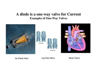
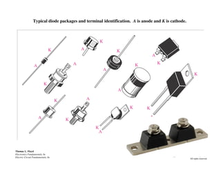
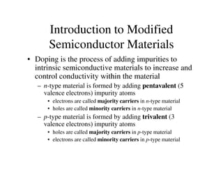
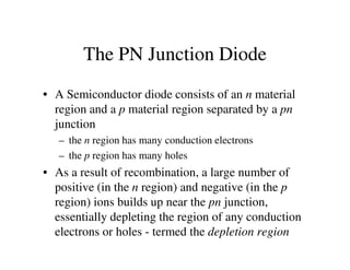
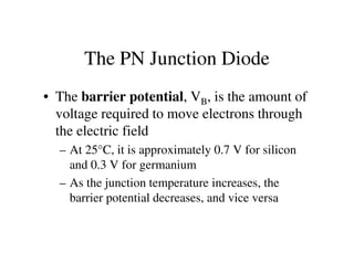
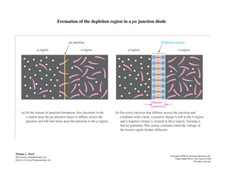
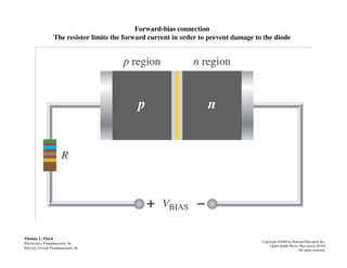
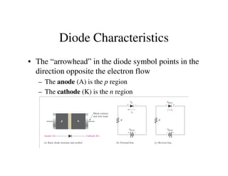

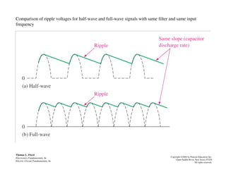
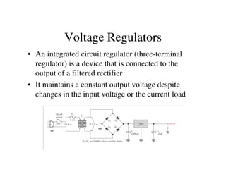
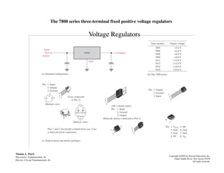
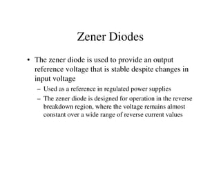
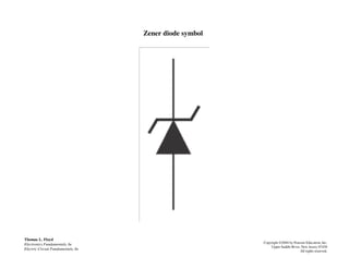
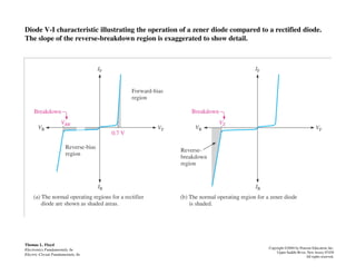
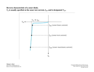
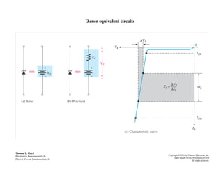
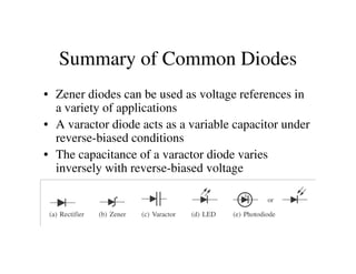

Semiconductors like silicon and germanium can be used to create diodes and transistors. A diode allows current to pass in only one direction, acting like a one-way valve. By adding impurities to an intrinsic semiconductor, n-type and p-type materials can be created. A PN junction diode consists of an n-type and p-type material joined together. Diodes can be used in rectifier circuits to convert AC to DC and in voltage regulators. Zener diodes operate in the reverse breakdown region to provide a stable reference voltage.


![[Deck] What's New in Spark-Iceberg Integration via DSV2.pptx](https://cdn.slidesharecdn.com/ss_thumbnails/deckwhatsnewinspark-icebergintegrationviadsv2-260210005337-25955b12-thumbnail.jpg?width=640&height=640&fit=bounds)


