Downloaded 1,376 times
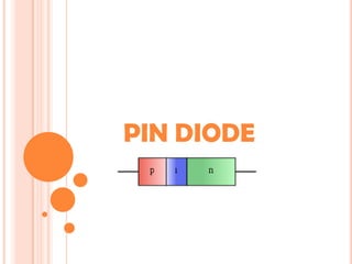
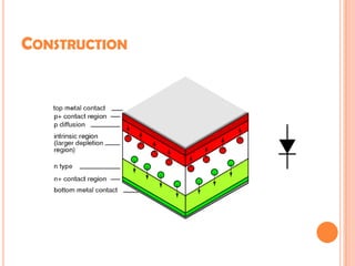
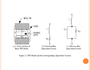
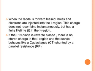
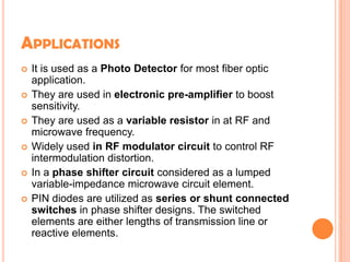
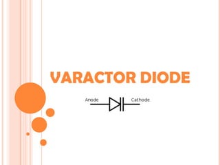
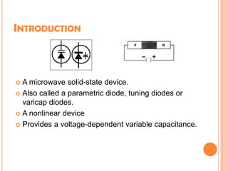


The document discusses PIN diodes and varactor diodes. A PIN diode has a wide intrinsic semiconductor region between a p-type and n-type region, making it suitable for applications like attenuators and switches. It operates as a variable resistor at radio frequencies. A varactor diode provides a voltage-dependent variable capacitance and is used for electronic tuning and frequency multiplication. Both diodes have applications in radio frequency circuits due to their ability to dynamically control signal properties.


