SlideShare a Scribd company logo
1 of 24
MADE BY GROUP 4
• BILAL HASSAN
• HAMZA ISMAIL MALIK
• ALI HASSAN ZAIDI
• MUHAMMAD ADNAN
• YOUNS NAQASH
TUNNEL DIODE
OUT LINES
HISTORY
DEFINITION
CONSTRUCTION
WORKING
APPLICATION
ADVANTAGE S AND DISADATAGES
HISTORY
• Tunnel Diode was invented in August 1957 by Leo Esaki.
• In 1973 he received the Nobel prize in physics for discovering
the electron tunneling effect used .
• well into the microwave frequency region, made possible by
the use of the quantum mechanical effect called tunneling.
Definition
• An extremely stable semiconductor diode, having a
very narrow highly doped p-n junction, in which
electrons travel across the junction by means of the
tunnel effect.
Construction
• There are several steps for this which are given below
1. Firstly, it reduces the width of the depletion layer to an
extremely small value (about 0.00001 mm).
2. Secondly, it reduces the reverse breakdown voltage to a very small
value (approaching zero) with the result that the diode appears to be
broken down for any reverse voltage.
construction
3. Thirdly, it produces a negative resistance section on the V/I
characteristic of the diode.
It is called a tunnel diode because due to its extremely thin
depletion layer, electrons are able to tunnel through the potential
barrier at relatively low forward bias voltage (less than 0.05V).
Such diodes are usually fabricated from germanium, gallium-
arsenide(GA As) and gallium antimonites (Gabs).
Tunnel diode symbol
Physical structure
V/I Characteristic
• As seen, forward bias produces immediate conduction
i.e. as soon as forward bias is applied, significant current
is produced.
• The current quickly rises touts peak value Ip when the
applied forward voltage reaches a valueVp (point A ).
V/I Characteristic
• When forward voltage is increased further, diode current starts
decreasing till it achieves its minimum value called valley current
Iv corresponding to valley voltageVv (point B).
• For voltages greater thanVv, current starts increasing again as in
any ordinary junction diode.
DIAGRAM
V/I Characteristic
• As seen from Fig between the peak point A and valley point B, current decreases
with increase in the applied voltage.
• In other words, tunnel diode possesses negative resistance (— R N) in this region.
• In fact, this constitutes the most useful property of the diode. Instead of
absorbing power, a negative resistance produces power.
• By offsetting losses in L and C components of a tank circuit, such a negative
resistance permits oscillations.
V/I Characteristic
• Hence, a tunnel diode is used as a very high frequency
oscillator.
• Another point worth noting is that this resistance increases as
we go from point A to B because as voltage is increased, current
keeps decreasing which means that diode negative resistance
keeps increasing.
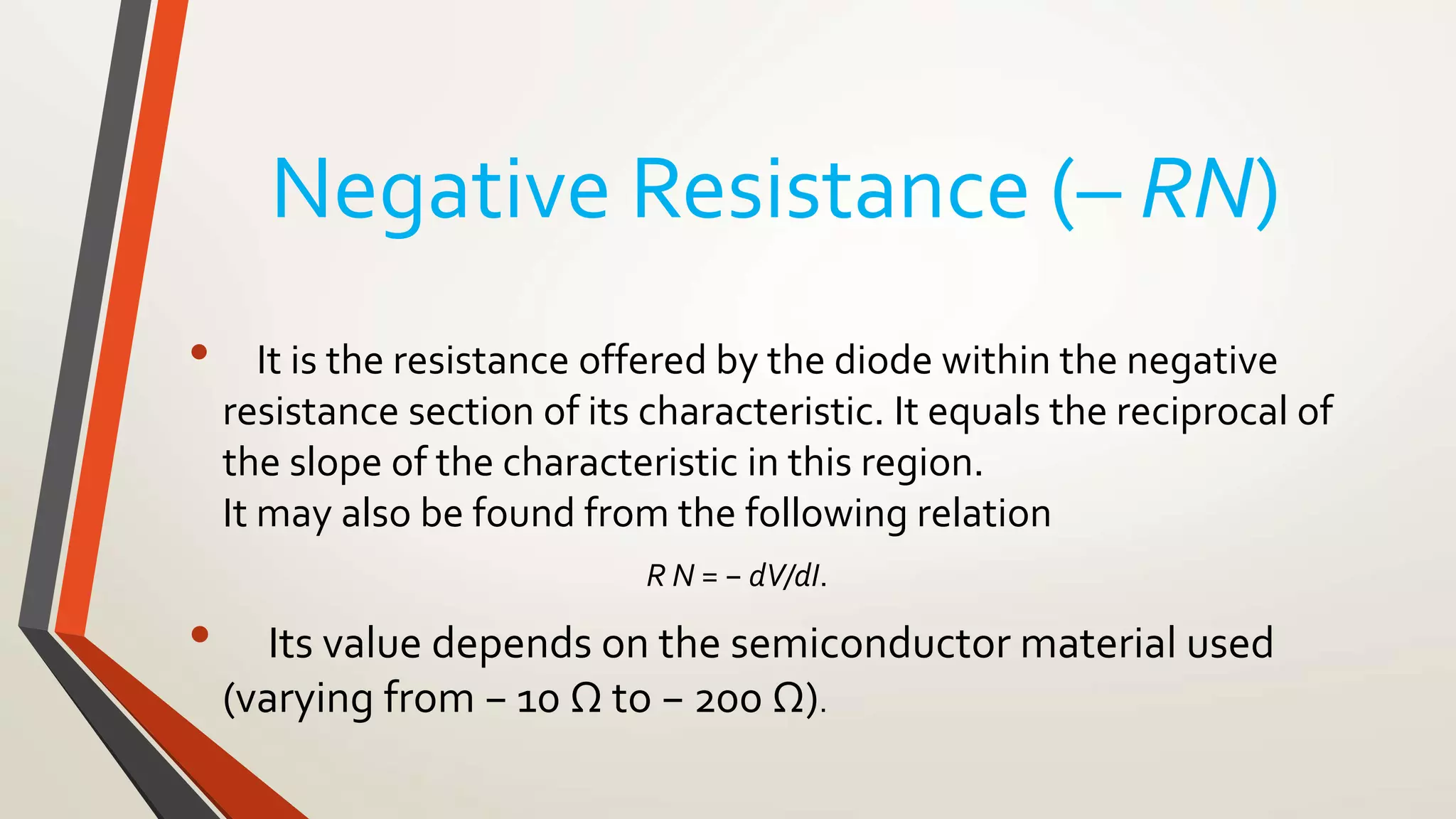
Negative Resistance (– RN)
• It is the resistance offered by the diode within the negative
resistance section of its characteristic. It equals the reciprocal of
the slope of the characteristic in this region.
It may also be found from the following relation
R N = − dV/dI.
• Its value depends on the semiconductor material used
(varying from − 10 Ω to − 200 Ω).
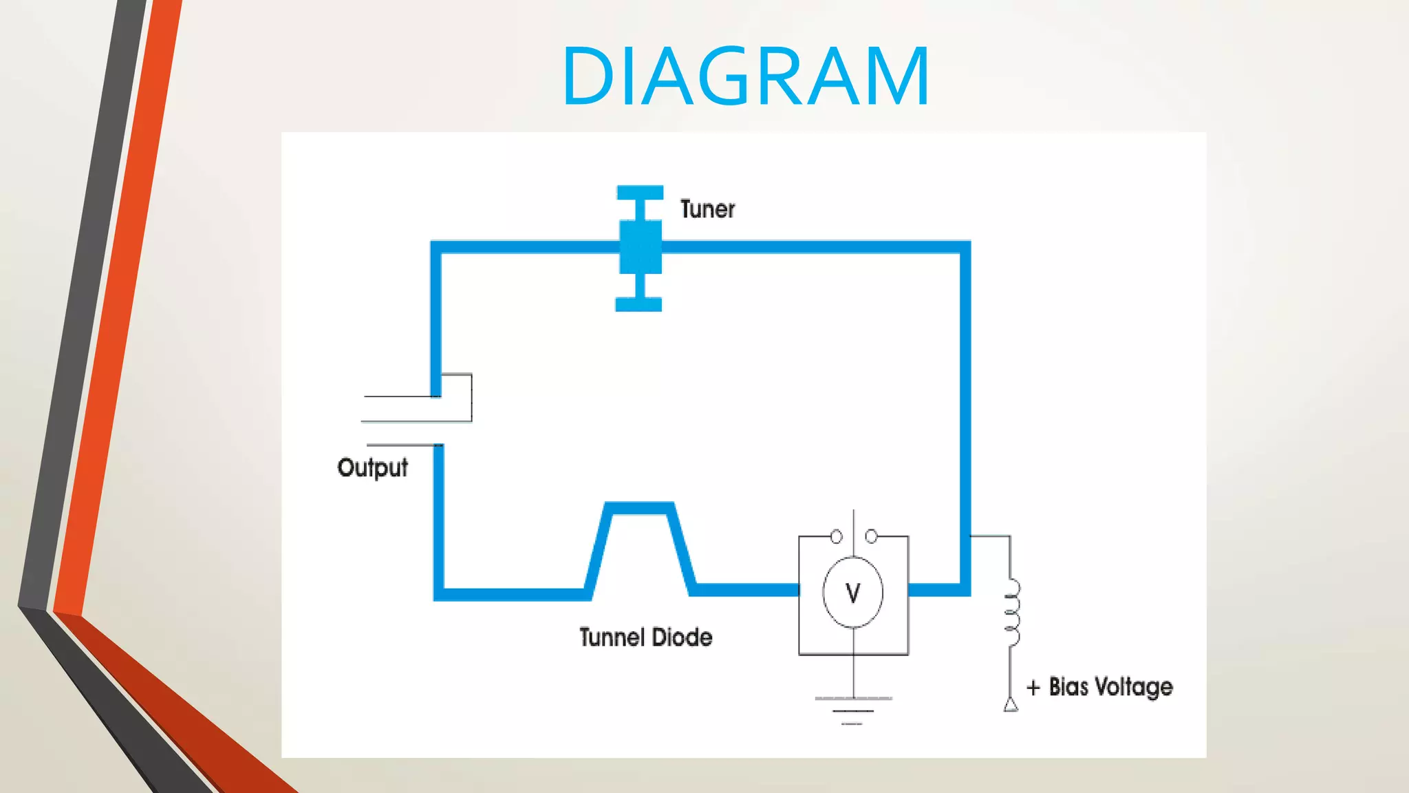
DIAGRAM
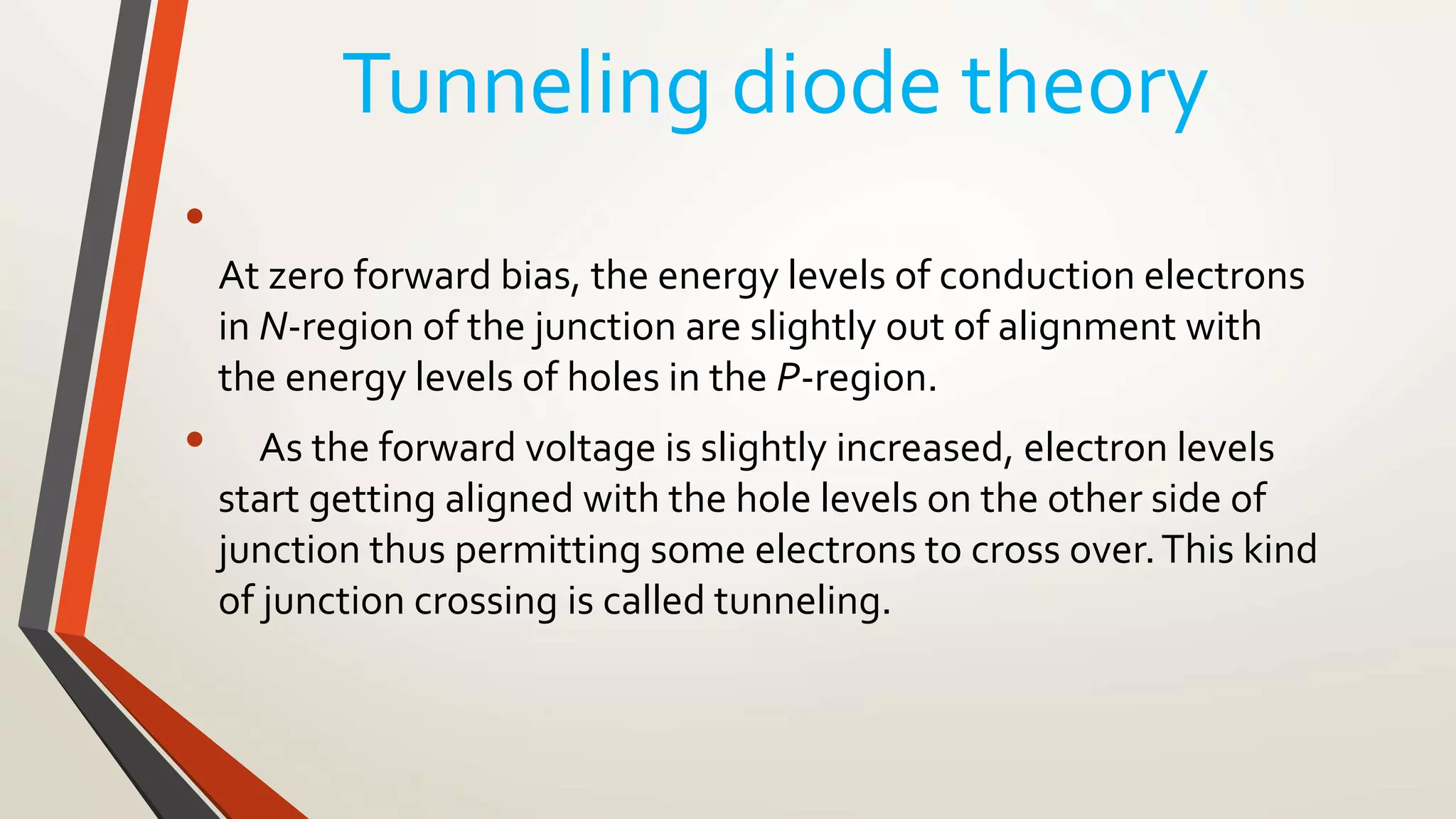
Tunneling diode theory
•
At zero forward bias, the energy levels of conduction electrons
in N-region of the junction are slightly out of alignment with
the energy levels of holes in the P-region.
• As the forward voltage is slightly increased, electron levels
start getting aligned with the hole levels on the other side of
junction thus permitting some electrons to cross over.This kind
of junction crossing is called tunneling.
Tunneling diode theory
• As voltage is increased to peak voltage (VP), all conduction
band electrons in the N-region are able to cross over to the
valence band in the P-region because the two bands are
exactly aligned. Hence, maximum current (called peak
current IP) flows in the circuit.
•After VP as the applied voltage is increased, current
starts decreasing because the two bands start
gradually getting out of alignment.
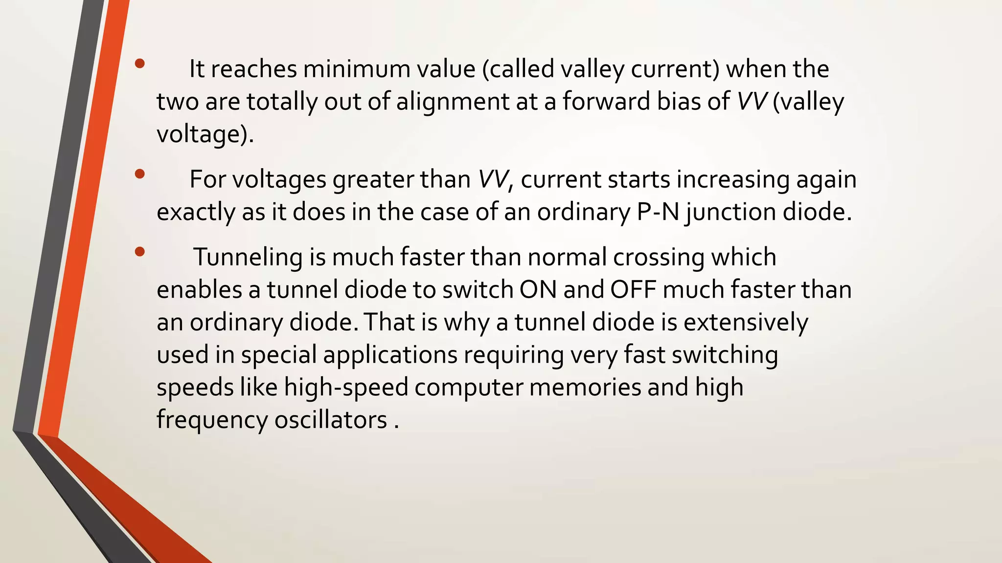
• It reaches minimum value (called valley current) when the
two are totally out of alignment at a forward bias of VV (valley
voltage).
• For voltages greater than VV, current starts increasing again
exactly as it does in the case of an ordinary P-N junction diode.
• Tunneling is much faster than normal crossing which
enables a tunnel diode to switch ON and OFF much faster than
an ordinary diode.That is why a tunnel diode is extensively
used in special applications requiring very fast switching
speeds like high-speed computer memories and high
frequency oscillators .
Backward diode applications
The characteristics of the backward diode make it suitable for a limited
number of applications where other diodes may not perform as well.
• Detector :
The backward diode provides a linear detection characteristic for small
signals. Additionally the fact that there is no charge storage in its mode of operation
means that it can be used for signals with frequencies extending to 50 GHz and more
Backward diode applications
• Rectifier:
The diode is suitable for rectifying signals with peak voltages between
about 0.1 and 0.6 volts.
• Switch:
In view of its speed of operation, the diode is sometimes used
for very high speed switching applications.
Advatages and disadvantages
• The advantages of a tunnel diode are :
• 1. low noise
• 2. ease of operation
• 3. high speed
• 4. low power
• 5. Insensitivity to nuclear radiations
Advatages and disadvantages
1. The voltage range over which it can be operated properly is 1V or less.
2. Being a two-terminal device, it provides no isolation between the input
and output circuits
SGH

More Related Content

What's hot (20)

Zener Diode Presentation
Zener Diode PresentationZener Diode Presentation
Zener Diode Presentation
 
Diode
DiodeDiode
Diode
 
TUNNEL DIODE
TUNNEL DIODETUNNEL DIODE
TUNNEL DIODE
 
Avalanche transit time devices
Avalanche transit time devicesAvalanche transit time devices
Avalanche transit time devices
 
Tunnel diode
Tunnel diodeTunnel diode
Tunnel diode
 
Analog Electronics ppt on Transition & diffusion capacitance by Being topper
Analog Electronics  ppt on Transition & diffusion capacitance by Being topperAnalog Electronics  ppt on Transition & diffusion capacitance by Being topper
Analog Electronics ppt on Transition & diffusion capacitance by Being topper
 
Hybrid Parameter in BJT
Hybrid Parameter in BJTHybrid Parameter in BJT
Hybrid Parameter in BJT
 
Transistor
TransistorTransistor
Transistor
 
Pn junction diodes (presentation)
Pn junction diodes (presentation)Pn junction diodes (presentation)
Pn junction diodes (presentation)
 
Zener and avalanche diode
Zener and avalanche diode    Zener and avalanche diode
Zener and avalanche diode
 
Scr basics
Scr   basicsScr   basics
Scr basics
 
Gun diode
Gun diodeGun diode
Gun diode
 
Lecture 2: Power Diodes
Lecture 2: Power DiodesLecture 2: Power Diodes
Lecture 2: Power Diodes
 
P n junction--eema
P n junction--eemaP n junction--eema
P n junction--eema
 
Diodes and Its Application
Diodes and Its ApplicationDiodes and Its Application
Diodes and Its Application
 
Pn junction diode
Pn junction diodePn junction diode
Pn junction diode
 
Semiconductor diode
Semiconductor diodeSemiconductor diode
Semiconductor diode
 
Field Effect Transistor
Field Effect TransistorField Effect Transistor
Field Effect Transistor
 
Wave guide tees
Wave guide teesWave guide tees
Wave guide tees
 
Diodes
Diodes Diodes
Diodes
 

Viewers also liked

Tunnel Diode (Esaki Diode )
Tunnel Diode (Esaki Diode )Tunnel Diode (Esaki Diode )
Tunnel Diode (Esaki Diode )Soudip Sinha Roy
 
les diodes particulieres
les diodes particulieresles diodes particulieres
les diodes particulieresAmel Chettah
 
Fstm deust mip-e141_cee_chap_vi_les diodes
Fstm deust mip-e141_cee_chap_vi_les diodesFstm deust mip-e141_cee_chap_vi_les diodes
Fstm deust mip-e141_cee_chap_vi_les diodesabdennaceur_baghdad
 
Impatt diode
Impatt diodeImpatt diode
Impatt diodeladdu13
 
Working principle diode and special diode
Working principle diode and special diodeWorking principle diode and special diode
Working principle diode and special diodeaman1894
 
Airport planning and Design
Airport planning and DesignAirport planning and Design
Airport planning and Designsrinivas2036
 
ELE2611 Classe 7 - Circuits non-linéaires statiques
ELE2611 Classe 7 - Circuits non-linéaires statiquesELE2611 Classe 7 - Circuits non-linéaires statiques
ELE2611 Classe 7 - Circuits non-linéaires statiquesJerome LE NY
 
SE1 - CM Composants - De la diode à l'ADI
SE1 - CM Composants - De la diode à l'ADISE1 - CM Composants - De la diode à l'ADI
SE1 - CM Composants - De la diode à l'ADIPierre Maréchal
 

Viewers also liked (15)

Tunnel Diode (Esaki Diode )
Tunnel Diode (Esaki Diode )Tunnel Diode (Esaki Diode )
Tunnel Diode (Esaki Diode )
 
Varactor diode
Varactor diodeVaractor diode
Varactor diode
 
les diodes particulieres
les diodes particulieresles diodes particulieres
les diodes particulieres
 
Tunnel diode sunum
Tunnel diode sunumTunnel diode sunum
Tunnel diode sunum
 
Fstm deust mip-e141_cee_chap_vi_les diodes
Fstm deust mip-e141_cee_chap_vi_les diodesFstm deust mip-e141_cee_chap_vi_les diodes
Fstm deust mip-e141_cee_chap_vi_les diodes
 
Diodes
DiodesDiodes
Diodes
 
Impatt diode
Impatt diodeImpatt diode
Impatt diode
 
Working principle diode and special diode
Working principle diode and special diodeWorking principle diode and special diode
Working principle diode and special diode
 
Trapatt diode
Trapatt diodeTrapatt diode
Trapatt diode
 
Airport engineering
Airport engineering Airport engineering
Airport engineering
 
Tunnel engineering
  Tunnel engineering  Tunnel engineering
Tunnel engineering
 
Airport planning and Design
Airport planning and DesignAirport planning and Design
Airport planning and Design
 
ELE2611 Classe 7 - Circuits non-linéaires statiques
ELE2611 Classe 7 - Circuits non-linéaires statiquesELE2611 Classe 7 - Circuits non-linéaires statiques
ELE2611 Classe 7 - Circuits non-linéaires statiques
 
Photodiode
PhotodiodePhotodiode
Photodiode
 
SE1 - CM Composants - De la diode à l'ADI
SE1 - CM Composants - De la diode à l'ADISE1 - CM Composants - De la diode à l'ADI
SE1 - CM Composants - De la diode à l'ADI
 

Similar to Tunnel diode(1)

12695 solid state m icrowave devices
12695 solid state m icrowave devices12695 solid state m icrowave devices
12695 solid state m icrowave devicesMohit Vyas
 
diode__description__tunnel__diode__.pptx
diode__description__tunnel__diode__.pptxdiode__description__tunnel__diode__.pptx
diode__description__tunnel__diode__.pptxVedanshiKaushik2
 
Microwave Devices q7.pptx
Microwave Devices q7.pptxMicrowave Devices q7.pptx
Microwave Devices q7.pptxGodwin308555
 
Electronic Devices - Special Diodes - Unit 1.pptx
Electronic Devices - Special Diodes - Unit 1.pptxElectronic Devices - Special Diodes - Unit 1.pptx
Electronic Devices - Special Diodes - Unit 1.pptxDhivya Ramachandran
 
Electronic devices circuits
Electronic devices circuitsElectronic devices circuits
Electronic devices circuitssudeep kumar
 
Optical Detectors.pptx
Optical Detectors.pptxOptical Detectors.pptx
Optical Detectors.pptxRajNivas3
 
tunneldiode by guru a s and suriya p k r
tunneldiode by guru a s and suriya p k rtunneldiode by guru a s and suriya p k r
tunneldiode by guru a s and suriya p k rsarkarf312
 
Diode data sheet for alarm type project
Diode data sheet for alarm type projectDiode data sheet for alarm type project
Diode data sheet for alarm type projectmegha agrawal
 
EST 130, PN Junction Diodes
EST 130, PN Junction DiodesEST 130, PN Junction Diodes
EST 130, PN Junction DiodesCKSunith1
 
Basic electronics and electrical first year engineering
Basic electronics and electrical first year engineeringBasic electronics and electrical first year engineering
Basic electronics and electrical first year engineeringron181295
 
Full sessional pack ii
Full sessional pack iiFull sessional pack ii
Full sessional pack iiUmer Tanvir
 

Similar to Tunnel diode(1) (20)

Special diodes.ppt
Special diodes.pptSpecial diodes.ppt
Special diodes.ppt
 
UNIT_5 PPT-MBM.pptx
UNIT_5 PPT-MBM.pptxUNIT_5 PPT-MBM.pptx
UNIT_5 PPT-MBM.pptx
 
UNIT4.pptx
UNIT4.pptxUNIT4.pptx
UNIT4.pptx
 
tunneldiode.pptx
tunneldiode.pptxtunneldiode.pptx
tunneldiode.pptx
 
12695 solid state m icrowave devices
12695 solid state m icrowave devices12695 solid state m icrowave devices
12695 solid state m icrowave devices
 
diode__description__tunnel__diode__.pptx
diode__description__tunnel__diode__.pptxdiode__description__tunnel__diode__.pptx
diode__description__tunnel__diode__.pptx
 
Microwave Devices q7.pptx
Microwave Devices q7.pptxMicrowave Devices q7.pptx
Microwave Devices q7.pptx
 
Electronic Devices - Special Diodes - Unit 1.pptx
Electronic Devices - Special Diodes - Unit 1.pptxElectronic Devices - Special Diodes - Unit 1.pptx
Electronic Devices - Special Diodes - Unit 1.pptx
 
Edcqnaunit 8
Edcqnaunit 8Edcqnaunit 8
Edcqnaunit 8
 
Electronic devices circuits
Electronic devices circuitsElectronic devices circuits
Electronic devices circuits
 
Optical Detectors.pptx
Optical Detectors.pptxOptical Detectors.pptx
Optical Detectors.pptx
 
Diode Applications.pptx
Diode Applications.pptxDiode Applications.pptx
Diode Applications.pptx
 
EC 8353 EDC
EC 8353 EDCEC 8353 EDC
EC 8353 EDC
 
tunneldiode by guru a s and suriya p k r
tunneldiode by guru a s and suriya p k rtunneldiode by guru a s and suriya p k r
tunneldiode by guru a s and suriya p k r
 
Diode data sheet for alarm type project
Diode data sheet for alarm type projectDiode data sheet for alarm type project
Diode data sheet for alarm type project
 
EST 130, PN Junction Diodes
EST 130, PN Junction DiodesEST 130, PN Junction Diodes
EST 130, PN Junction Diodes
 
P n junction diode prabhakar
P n junction diode prabhakar P n junction diode prabhakar
P n junction diode prabhakar
 
Basic electronics and electrical first year engineering
Basic electronics and electrical first year engineeringBasic electronics and electrical first year engineering
Basic electronics and electrical first year engineering
 
Full sessional pack ii
Full sessional pack iiFull sessional pack ii
Full sessional pack ii
 
5 diodes
5  diodes5  diodes
5 diodes
 

More from 03470719974

special types of diodes Tunnel diode(1)
 special types of diodes Tunnel diode(1) special types of diodes Tunnel diode(1)
special types of diodes Tunnel diode(1)03470719974
 
Planing of effective message
Planing of effective messagePlaning of effective message
Planing of effective message03470719974
 
Standard parts of letter
Standard parts of letterStandard parts of letter
Standard parts of letter03470719974
 

More from 03470719974 (7)

Lecture 3
Lecture 3Lecture 3
Lecture 3
 
Lecture 2
Lecture 2Lecture 2
Lecture 2
 
Lecture 1
Lecture 1Lecture 1
Lecture 1
 
special types of diodes Tunnel diode(1)
 special types of diodes Tunnel diode(1) special types of diodes Tunnel diode(1)
special types of diodes Tunnel diode(1)
 
Planing of effective message
Planing of effective messagePlaning of effective message
Planing of effective message
 
Standard parts of letter
Standard parts of letterStandard parts of letter
Standard parts of letter
 
Body language
Body languageBody language
Body language
 

Tunnel diode(1)

  • 1.
  • 2. MADE BY GROUP 4 • BILAL HASSAN • HAMZA ISMAIL MALIK • ALI HASSAN ZAIDI • MUHAMMAD ADNAN • YOUNS NAQASH
  • 5. HISTORY • Tunnel Diode was invented in August 1957 by Leo Esaki. • In 1973 he received the Nobel prize in physics for discovering the electron tunneling effect used . • well into the microwave frequency region, made possible by the use of the quantum mechanical effect called tunneling.
  • 6. Definition • An extremely stable semiconductor diode, having a very narrow highly doped p-n junction, in which electrons travel across the junction by means of the tunnel effect.
  • 7. Construction • There are several steps for this which are given below 1. Firstly, it reduces the width of the depletion layer to an extremely small value (about 0.00001 mm). 2. Secondly, it reduces the reverse breakdown voltage to a very small value (approaching zero) with the result that the diode appears to be broken down for any reverse voltage.
  • 8. construction 3. Thirdly, it produces a negative resistance section on the V/I characteristic of the diode. It is called a tunnel diode because due to its extremely thin depletion layer, electrons are able to tunnel through the potential barrier at relatively low forward bias voltage (less than 0.05V). Such diodes are usually fabricated from germanium, gallium- arsenide(GA As) and gallium antimonites (Gabs).
  • 10. V/I Characteristic • As seen, forward bias produces immediate conduction i.e. as soon as forward bias is applied, significant current is produced. • The current quickly rises touts peak value Ip when the applied forward voltage reaches a valueVp (point A ).
  • 11. V/I Characteristic • When forward voltage is increased further, diode current starts decreasing till it achieves its minimum value called valley current Iv corresponding to valley voltageVv (point B). • For voltages greater thanVv, current starts increasing again as in any ordinary junction diode.
  • 13. V/I Characteristic • As seen from Fig between the peak point A and valley point B, current decreases with increase in the applied voltage. • In other words, tunnel diode possesses negative resistance (— R N) in this region. • In fact, this constitutes the most useful property of the diode. Instead of absorbing power, a negative resistance produces power. • By offsetting losses in L and C components of a tank circuit, such a negative resistance permits oscillations.
  • 14. V/I Characteristic • Hence, a tunnel diode is used as a very high frequency oscillator. • Another point worth noting is that this resistance increases as we go from point A to B because as voltage is increased, current keeps decreasing which means that diode negative resistance keeps increasing.
  • 15. Negative Resistance (– RN) • It is the resistance offered by the diode within the negative resistance section of its characteristic. It equals the reciprocal of the slope of the characteristic in this region. It may also be found from the following relation R N = − dV/dI. • Its value depends on the semiconductor material used (varying from − 10 Ω to − 200 Ω).
  • 17. Tunneling diode theory • At zero forward bias, the energy levels of conduction electrons in N-region of the junction are slightly out of alignment with the energy levels of holes in the P-region. • As the forward voltage is slightly increased, electron levels start getting aligned with the hole levels on the other side of junction thus permitting some electrons to cross over.This kind of junction crossing is called tunneling.
  • 18. Tunneling diode theory • As voltage is increased to peak voltage (VP), all conduction band electrons in the N-region are able to cross over to the valence band in the P-region because the two bands are exactly aligned. Hence, maximum current (called peak current IP) flows in the circuit. •After VP as the applied voltage is increased, current starts decreasing because the two bands start gradually getting out of alignment.
  • 19. • It reaches minimum value (called valley current) when the two are totally out of alignment at a forward bias of VV (valley voltage). • For voltages greater than VV, current starts increasing again exactly as it does in the case of an ordinary P-N junction diode. • Tunneling is much faster than normal crossing which enables a tunnel diode to switch ON and OFF much faster than an ordinary diode.That is why a tunnel diode is extensively used in special applications requiring very fast switching speeds like high-speed computer memories and high frequency oscillators .
  • 20. Backward diode applications The characteristics of the backward diode make it suitable for a limited number of applications where other diodes may not perform as well. • Detector : The backward diode provides a linear detection characteristic for small signals. Additionally the fact that there is no charge storage in its mode of operation means that it can be used for signals with frequencies extending to 50 GHz and more
  • 21. Backward diode applications • Rectifier: The diode is suitable for rectifying signals with peak voltages between about 0.1 and 0.6 volts. • Switch: In view of its speed of operation, the diode is sometimes used for very high speed switching applications.
  • 22. Advatages and disadvantages • The advantages of a tunnel diode are : • 1. low noise • 2. ease of operation • 3. high speed • 4. low power • 5. Insensitivity to nuclear radiations
  • 23. Advatages and disadvantages 1. The voltage range over which it can be operated properly is 1V or less. 2. Being a two-terminal device, it provides no isolation between the input and output circuits
  • 24. SGH