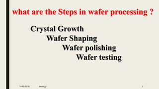
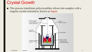
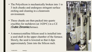
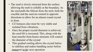
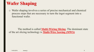
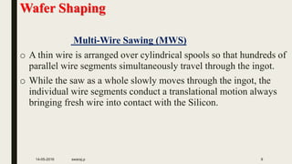
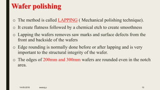
WAFER
PROCESSING
SWARAJ P
Dept. of Electronics and Communication
Govt. Engineering College Thrissur
What is Wafer Processing ?
o Wafer process is a procedure composed of many repeated
sequential processes to produce complete electrical or
photonic circuits
o The silicon crystal is manufactured as a
cylinder with a diameter of 8-12inches.This
cylinder is carefully sawed into thin disks
called wafers, which are later polished and
marked for crystal orientation.
.
14-05-2016 swaraj.p 2
what are the Steps in wafer processing ?
Crystal Growth
Wafer Shaping
Wafer polishing
Wafer testing
14-05-2016 swaraj.p 3
Why Crystal Growth method?
• MG-Si is reacted with HCl to form trichlorosilane (TCS) in a fluidized-
bed reactor (300oC)
Si + 3HCl --> SiHCl3 + H2.
• TCS is an intermediate compound for polysilicon manufacturing.
• Impurities such as Fe, Al and B are removed.
• this ultra-pure TCS is subsequently vaporized ,diluted with H2, and
flowed into a deposition reactor where it is retransformed into elemental
silicon.
• This polysilicon has typical contamination levels of less than .001 ppb.
• But cristal grouth method provide high purity silicon (99.999999999%
eleven nines)
14-05-2016 swaraj.p 4
Crystal Growth
■ This process transforms polycrystalline silicon into samples with a
singular crystal orientation, known as Ingots
14-05-2016 swaraj.p 5
• The Polysilicon is mechanically broken into 1 to
3 inch chunks and undergoes stringent surface
etching and cleaning in a cleanroom
environment.
• These chunks are then packed into quartz
crucibles for meltdown (at 1420oC) in a CZ
(Cubic Zirconia)furnace.
• A monocrystalline Silicon seed is installed into
a seed shaft in the upper chamber of the furnace.
Slowly, the seed is lowered so that it dips
approximately 2mm into the Silicon melt.
14-05-2016 swaraj.p 6
• The seed is slowly retracted from the surface
allowing the melt to solidify at the boundary. As
the seed pulls the Silicon from the melt, both the
crucible and the seed are rotated in opposite
directions to allow for an almost round crystal
to form.
• CZ furnaces also must be very stable and
isolated from vibrations.
• Once the proper crystal diameter is achieved,
the seed lift is increased. This, along with the
heat transfer from heater elements will control
the diameter of the crystal
• This gradual cooling allows the crystal lattice
to stabilize and makes handling easier before
transport to the next operation14-05-2016 swaraj.p 7
Wafer Shaping
o Wafer shaping involves a series of precise mechanical and chemical
process steps that are necessary to turn the ingot segment into a
functional wafer.
The method is called Multi-Wiring Slicing. The dominant state
of the art slicing technology is Multi-Wire Sawing (MWS)
14-05-2016 swaraj.p 8
Wafer Shaping
Multi-Wire Sawing (MWS)
o A thin wire is arranged over cylindrical spools so that hundreds of
parallel wire segments simultaneously travel through the ingot.
o While the saw as a whole slowly moves through the ingot, the
individual wire segments conduct a translational motion always
bringing fresh wire into contact with the Silicon.
14-05-2016 swaraj.p 9
Wafer polishing
o The method is called LAPPING ( Mechanical polishing technique).
o It create flatness followed by a chemical etch to create smoothness
o Lapping the wafers removes saw marks and surface defects from the
front and backside of the wafers
o Edge rounding is normally done before or after lapping and is very
important to the structural integrity of the wafer.
o The edges of 200mm and 300mm wafers are rounded even in the notch
area.
14-05-2016 swaraj.p 10
THANK YOU 
14-05-2016 swaraj.p 11

Wafer processing

  • 1.
    WAFER PROCESSING SWARAJ P Dept. ofElectronics and Communication Govt. Engineering College Thrissur
  • 2.
    What is WaferProcessing ? o Wafer process is a procedure composed of many repeated sequential processes to produce complete electrical or photonic circuits o The silicon crystal is manufactured as a cylinder with a diameter of 8-12inches.This cylinder is carefully sawed into thin disks called wafers, which are later polished and marked for crystal orientation. . 14-05-2016 swaraj.p 2
  • 3.
    what are theSteps in wafer processing ? Crystal Growth Wafer Shaping Wafer polishing Wafer testing 14-05-2016 swaraj.p 3
  • 4.
    Why Crystal Growthmethod? • MG-Si is reacted with HCl to form trichlorosilane (TCS) in a fluidized- bed reactor (300oC) Si + 3HCl --> SiHCl3 + H2. • TCS is an intermediate compound for polysilicon manufacturing. • Impurities such as Fe, Al and B are removed. • this ultra-pure TCS is subsequently vaporized ,diluted with H2, and flowed into a deposition reactor where it is retransformed into elemental silicon. • This polysilicon has typical contamination levels of less than .001 ppb. • But cristal grouth method provide high purity silicon (99.999999999% eleven nines) 14-05-2016 swaraj.p 4
  • 5.
    Crystal Growth ■ Thisprocess transforms polycrystalline silicon into samples with a singular crystal orientation, known as Ingots 14-05-2016 swaraj.p 5
  • 6.
    • The Polysiliconis mechanically broken into 1 to 3 inch chunks and undergoes stringent surface etching and cleaning in a cleanroom environment. • These chunks are then packed into quartz crucibles for meltdown (at 1420oC) in a CZ (Cubic Zirconia)furnace. • A monocrystalline Silicon seed is installed into a seed shaft in the upper chamber of the furnace. Slowly, the seed is lowered so that it dips approximately 2mm into the Silicon melt. 14-05-2016 swaraj.p 6
  • 7.
    • The seedis slowly retracted from the surface allowing the melt to solidify at the boundary. As the seed pulls the Silicon from the melt, both the crucible and the seed are rotated in opposite directions to allow for an almost round crystal to form. • CZ furnaces also must be very stable and isolated from vibrations. • Once the proper crystal diameter is achieved, the seed lift is increased. This, along with the heat transfer from heater elements will control the diameter of the crystal • This gradual cooling allows the crystal lattice to stabilize and makes handling easier before transport to the next operation14-05-2016 swaraj.p 7
  • 8.
    Wafer Shaping o Wafershaping involves a series of precise mechanical and chemical process steps that are necessary to turn the ingot segment into a functional wafer. The method is called Multi-Wiring Slicing. The dominant state of the art slicing technology is Multi-Wire Sawing (MWS) 14-05-2016 swaraj.p 8
  • 9.
    Wafer Shaping Multi-Wire Sawing(MWS) o A thin wire is arranged over cylindrical spools so that hundreds of parallel wire segments simultaneously travel through the ingot. o While the saw as a whole slowly moves through the ingot, the individual wire segments conduct a translational motion always bringing fresh wire into contact with the Silicon. 14-05-2016 swaraj.p 9
  • 10.
    Wafer polishing o Themethod is called LAPPING ( Mechanical polishing technique). o It create flatness followed by a chemical etch to create smoothness o Lapping the wafers removes saw marks and surface defects from the front and backside of the wafers o Edge rounding is normally done before or after lapping and is very important to the structural integrity of the wafer. o The edges of 200mm and 300mm wafers are rounded even in the notch area. 14-05-2016 swaraj.p 10
  • 11.