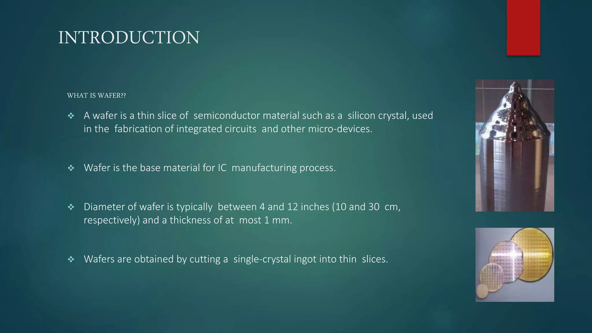
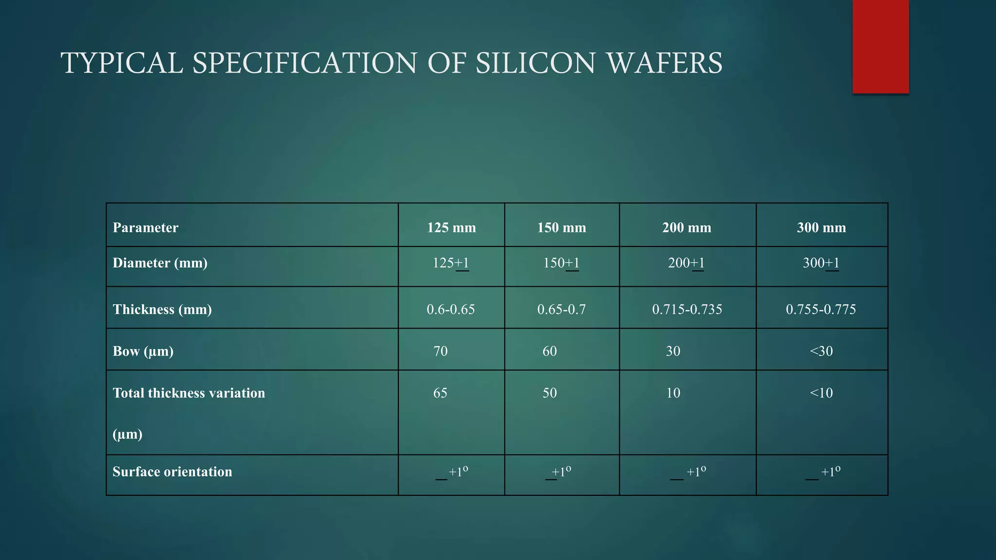
WAFER PREPARATION
PRESENTED BY: SOMIT SAMANTO
CLASS ROLL NO:ECE2015/058
UNIVERSITY ROLL NO: 11700315096
CONTENTS
 INTRODUCTION …………………………………………………………………………………..3
 WAFER PROPERTIES……………………………………………………………………………...4
 WAFER IDENTIFICATION…………………………………………………………………….....5
 PREPARATION OF SILICON WAFER………………………………………………………….6
 WAFER ETCHING…………………………………………………………………………………….7
 WAFER PLANARIZATION………………………………………………………………………….8
 WAFER POLISHING…………………………………………………………………………….......9
 WAFER SPECIFICATION…………………………………………………………………….........11
 CONCLUSION…………………………………………………………………………………………..12
INTRODUCTION
WHAT IS WAFER??
 A wafer is a thin slice of semiconductor material such as a silicon crystal, used
in the fabrication of integrated circuits and other micro-devices.
 Wafer is the base material for IC manufacturing process.
 Diameter of wafer is typically between 4 and 12 inches (10 and 30 cm,
respectively) and a thickness of at most 1 mm.
 Wafers are obtained by cutting a single-crystal ingot into thin slices.
WAFER PROPERTIES
 Silicon wafer must be in the form of a single-crystalline, lightly doped wafer.
 The surface of the wafer is doped more heavily and a single crystal epitaxial layer of the
opposite type is grown over the surface.
 Diameter of wafer Is typically between 4 and 12 inches (10 and 30 cm, respectively) and a
thickness of at most 1 mm
WAFER IDENTIFICATION
Preparation of Silicon Wafer
1. Crystal Growth
2. Single Crystal
Ingot
3. Crystal Trimming
and Diameter
Grind
4. Flat Grinding
5. Wafer Slicing
6. Edge Rounding
7. Lapping
8. Wafer Etching
9. Polishing
10. Wafer Inspection
Slurry
Polishing table
Polishing
head
Polysilicon Seed crystal
Heater
Crucible
WAFER ETCHING
Etching is a process of selectively removing the
unwanted material from the surface of the wafer.
When etching is performed, the etchant may remove
portions or all of:
• The desired material
• The underlying layer
• The masking layer
There are basically two types of etches:
• Wet etch which uses chemicals
• Dry etch which uses chemically active ionized
gases/plasma.
WAFER PLANARIZATION
Planarization attempts to minimize the variation in
surface height of the wafer.
Planarization techniques
•Repeated applications of spin-on-glass (SOG).
•Resist etch-back – highest areas of oxide are exposed
longest to the etchant and therefore erode away the
most.
A chemical-mechanical planarization (CMP) step is
included before the deposition of an extra metal layer
on top of the insulating SiO2 layer.
Wafer polishing
Polishing is the final step. Its purpose is to provide a smooth, specular surface on which device features can be
photoengraved. Figure 2.13 depicts the schematic of a typical polishing machine and the process. Figure 2.14
displays finished silicon wafers of various dimensions. A finished wafer is subject to a myriad of tolerences.
fig:2.13 schematic of polishing process
continued…
Finished silicon wafer of various sizes.
TYPICAL SPECIFICATION OF SILICON WAFERS
Parameter 125 mm 150 mm 200 mm 300 mm
Diameter (mm) 125+1 150+1 200+1 300+1
Thickness (mm) 0.6-0.65 0.65-0.7 0.715-0.735 0.755-0.775
Bow (µm) 70 60 30 <30
Total thickness variation 65 50 10 <10
(µm)
Surface orientation +1o +1o +1o +1o
CONCLUSION
Thus,wafer, also called a slice or substrate,is a thin slice of semiconductor material, such
as a crystalline silicon , used in electronics for the fabrication of integrated circuits and
in photovoltaics for conventional, wafer-based solar cells . The wafer serves as
the substrate for microelectronic devices built in and over the wafer and undergoes
many microfabrication ,process steps such as doping or ion
implantation, etching, deposition of various materials,
and photolithographic patterning. Finally, the individual microcircuits are separated
and packaged.Therefore ,this presentation show how wafer can be prepared

Wafer preparation

  • 1.
    WAFER PREPARATION PRESENTED BY:SOMIT SAMANTO CLASS ROLL NO:ECE2015/058 UNIVERSITY ROLL NO: 11700315096
  • 2.
    CONTENTS  INTRODUCTION …………………………………………………………………………………..3 WAFER PROPERTIES……………………………………………………………………………...4  WAFER IDENTIFICATION…………………………………………………………………….....5  PREPARATION OF SILICON WAFER………………………………………………………….6  WAFER ETCHING…………………………………………………………………………………….7  WAFER PLANARIZATION………………………………………………………………………….8  WAFER POLISHING…………………………………………………………………………….......9  WAFER SPECIFICATION…………………………………………………………………….........11  CONCLUSION…………………………………………………………………………………………..12
  • 3.
    INTRODUCTION WHAT IS WAFER?? A wafer is a thin slice of semiconductor material such as a silicon crystal, used in the fabrication of integrated circuits and other micro-devices.  Wafer is the base material for IC manufacturing process.  Diameter of wafer is typically between 4 and 12 inches (10 and 30 cm, respectively) and a thickness of at most 1 mm.  Wafers are obtained by cutting a single-crystal ingot into thin slices.
  • 4.
    WAFER PROPERTIES  Siliconwafer must be in the form of a single-crystalline, lightly doped wafer.  The surface of the wafer is doped more heavily and a single crystal epitaxial layer of the opposite type is grown over the surface.  Diameter of wafer Is typically between 4 and 12 inches (10 and 30 cm, respectively) and a thickness of at most 1 mm
  • 5.
  • 6.
    Preparation of SiliconWafer 1. Crystal Growth 2. Single Crystal Ingot 3. Crystal Trimming and Diameter Grind 4. Flat Grinding 5. Wafer Slicing 6. Edge Rounding 7. Lapping 8. Wafer Etching 9. Polishing 10. Wafer Inspection Slurry Polishing table Polishing head Polysilicon Seed crystal Heater Crucible
  • 7.
    WAFER ETCHING Etching isa process of selectively removing the unwanted material from the surface of the wafer. When etching is performed, the etchant may remove portions or all of: • The desired material • The underlying layer • The masking layer There are basically two types of etches: • Wet etch which uses chemicals • Dry etch which uses chemically active ionized gases/plasma.
  • 8.
    WAFER PLANARIZATION Planarization attemptsto minimize the variation in surface height of the wafer. Planarization techniques •Repeated applications of spin-on-glass (SOG). •Resist etch-back – highest areas of oxide are exposed longest to the etchant and therefore erode away the most. A chemical-mechanical planarization (CMP) step is included before the deposition of an extra metal layer on top of the insulating SiO2 layer.
  • 9.
    Wafer polishing Polishing isthe final step. Its purpose is to provide a smooth, specular surface on which device features can be photoengraved. Figure 2.13 depicts the schematic of a typical polishing machine and the process. Figure 2.14 displays finished silicon wafers of various dimensions. A finished wafer is subject to a myriad of tolerences. fig:2.13 schematic of polishing process
  • 10.
  • 11.
    TYPICAL SPECIFICATION OFSILICON WAFERS Parameter 125 mm 150 mm 200 mm 300 mm Diameter (mm) 125+1 150+1 200+1 300+1 Thickness (mm) 0.6-0.65 0.65-0.7 0.715-0.735 0.755-0.775 Bow (µm) 70 60 30 <30 Total thickness variation 65 50 10 <10 (µm) Surface orientation +1o +1o +1o +1o
  • 12.
    CONCLUSION Thus,wafer, also calleda slice or substrate,is a thin slice of semiconductor material, such as a crystalline silicon , used in electronics for the fabrication of integrated circuits and in photovoltaics for conventional, wafer-based solar cells . The wafer serves as the substrate for microelectronic devices built in and over the wafer and undergoes many microfabrication ,process steps such as doping or ion implantation, etching, deposition of various materials, and photolithographic patterning. Finally, the individual microcircuits are separated and packaged.Therefore ,this presentation show how wafer can be prepared