Downloaded 252 times


![Micro Devices:Microgear and Alignment Pin
[Courtesy of Sandia National Laboratories]
Alignment Pin
Gear
Substrate
6](https://image.slidesharecdn.com/etchingprocessesformicrosystemsfabrication-150129072212-conversion-gate01/85/Etching-processes-for-microsystems-fabrication-6-320.jpg)


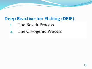


The document discusses various etching processes involved in microsystems fabrication, specifically focusing on wet and dry etching techniques, including the Bosch and cryogenic processes. It addresses key parameters like etch rate and selectivity, and highlights the challenges associated with these methods, such as notching effects and variations in etching depth. Overall, it emphasizes the importance of understanding these etching processes and their parameters for successful microsystems development.


