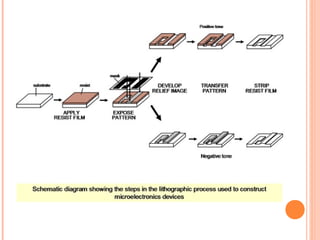
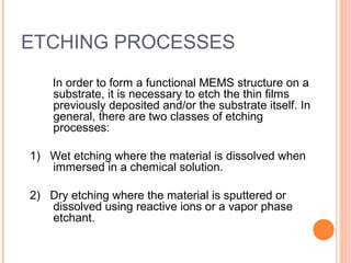
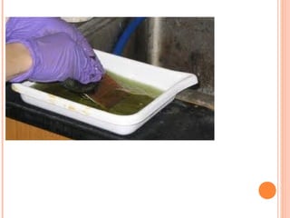
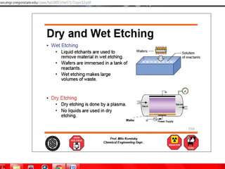
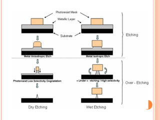
MEMS 
FBRICATION 
METHODS 
MADE BY: Amit . K. Parcha 
Roll No:2K13E21 
Department of Electronic Science 
Uinversity Of Pune
TABLE OF CONTENTS 
Abstract of work undertaken 
3) Introduction to the problem 
4) Fabricating MEMS and Nanotechnology 
a) Deposition Processes 
b) Lithography 
c) Etching 
MEMS and Nanotechnology Applications 
6) Current Challenges 
Reference sites
MEMS: MICRO-ELECTRO-MECHANICAL 
SYSTEMS 
COMBINATION OF MECHANICAL 
FUNCTIONS 
(SENSING,MOVING,HEATING) AND 
ELECTRICAL FUNCTIONS 
(SWITCHING ,DECIDING) ON THE SAME 
CHIP USING MICRO FABRICATION 
TECHNOLOGY.
INTRODUCTION TO THE PROBLEM 
 Imagine a machine so small that it is imperceptible to the 
human eye. Imagine working machines no bigger than a 
grain of pollen. Imagine thousands of these machines batch 
fabricated on a single piece of silicon, for just a few pennies 
each. Imagine a world where gravity and inertia are no 
longer important, but atomic forces and surface science 
dominate. Imagine a silicon chip with thousands of 
microscopic mirrors working in unison, enabling the all optical 
network and removing the bottlenecks from the global 
telecommunications infrastructure. You are now entering the 
microdomain, a world occupied by an explosive technology 
known as MEMS. A world of challenge and opportunity, 
where traditional engineering concepts are turned upside 
down, and the realm of the "possible" is totally redefined.
FABRICATING MEMS AND 
NANOTECHNOLOGY 
 MEMS technology is based on a number of tools and 
methodologies, which are used to form small structures with 
dimensions in the micrometer scale (one millionth of a meter). 
Significant parts of the technology has been adopted from 
integrated circuit (IC) technology. For instance, almost all devices 
are build on wafers of silicon, like ICs. The structures are realized 
in thin films of materials, like ICs. They are patterned using 
photolithographic methods, like ICs. There are however several 
processes that are not derived from IC technology, and as the 
technology continues to grow the gap with IC technology also 
grows. 
 There are three basic building blocks in MEMS technology, which 
are the ability to deposit thin films of material on a substrate, to 
apply a patterned mask on top of the films by photolithograpic 
imaging, and to etch the films selectively to the mask. A MEMS 
process is usually a structured sequence of these operations to 
form actual devices.
DEPOSITION PROCESSES 
MEMS Thin Film Deposition Processes 
One of the basic building blocks in MEMS processing is the ability to deposit thin films of material. 
In this text we assume a thin film to have a thickness anywhere between a few nanometer to 
about 100 micrometer. 
MEMS deposition technology can be classified in two groups: 
1. Depositions that happen because of a chemical reaction: 
a) Chemical Vapor Deposition (CVD) 
b) Electrodeposition 
c) Epitaxy 
d) Thermal oxidation 
These processes exploit the creation of solid materials directly from chemical reactions in gas 
and/or liquid compositions or with the substrate material. The solid material is usually not the only 
product formed by the reaction. Byproducts can include gases, liquids and even other solids. 
2) Depositions that happen because of a physical reaction: 
a) Physical Vapor Deposition (PVD) 
b) Casting
LITHOGRAPHY 
Various steps involved in Lithography: 
1) Pattern Transfer 
Lithography in the MEMS context is typically the transfer of a pattern to a photosensitive material 
by selective exposure to a radiation source such as light. A photosensitive material is a material 
that experiences a change in its physical properties when exposed to a radiation source. If we 
selectively expose a photosensitive material to radiation (e.g. by masking some of the radiation) 
the pattern of the radiation on the material is transferred to the material exposed, as the 
properties of the exposed and unexposed regions differs. 
2) Alignment 
In order to make useful devices the patterns for different lithography steps that belong to a single 
structure must be aligned to one another. The first pattern transferred to a wafer usually 
includes a set of alignment marks, which are high precision features that are used as the 
reference when positioning subsequent patterns, to the first pattern. 
3) Exposure 
The exposure parameters required in order to achieve accurate pattern transfer from the mask to 
the photosensitive layer depend primarily on the wavelength of the radiation source and the 
dose required to achieve the desired properties change of the photoresist. Different photoresists 
exhibit different sensitivities to different wavelengths. The dose required per unit volume of 
photoresist for good pattern transfer is somewhat constant; however, the physics of the 
exposure process may affect the dose actually received. For example a highly reflective layer 
under the photoresist may result in the material experiencing a higher dose than if the 
underlying layer is absorptive, as the photoresist is exposed both by the incident radiation as 
well as the reflected radiation. The dose will also vary with resist thickness.
ETCHING PROCESSES 
In order to form a functional MEMS structure on a 
substrate, it is necessary to etch the thin films 
previously deposited and/or the substrate itself. In 
general, there are two classes of etching 
processes: 
1) Wet etching where the material is dissolved when 
immersed in a chemical solution. 
2) Dry etching where the material is sputtered or 
dissolved using reactive ions or a vapor phase 
etchant.
Other Microfabrication 
Processes 
1)Soft lithography 
2)Micro-Imprint 
Lithography 
3)Microstereolithography 
(MSTL
Base material of MEMS 
¾ Single crystal wafers 
- Diameter of 4‘‘ to 6‘‘ 
- Thickness 200 μm to 1 mm 
- Orientation mostly <110> and <100>
COMPARISON OF 
MICROELECTRONICS AND 
MICROSYSTEMS 
Microelectronics Microsystems (silicon 
 Fabrication 
techniques are proven 
and well documented 
 Packaging technology 
is relatively well 
established 
 Primarily 2- 
dimensional 
structures 
 Stationary structures 
based) 
 Many microfabrication 
techniques are used for 
production, but with no 
standard procedures 
 Packaging technology is 
Complex 
 3-dimensional structure 
at the infant stage 
 May involve moving 
components
ADVANTAGES: 
Less material usage 
Lower power requirements 
Greater functionality per unit space 
Accessibility to regions that are forbidden to 
larger products 
In most cases, smaller products should mean 
lower prices because less material is used
MATERIALS FOR MEMS 
1)Materials are the basic things 
required to develop micro 
sensors 
2)Metals 
3)Polymers 
4)Ceramic materials 
5)Semiconductors 
6)Composite materials
mems product is always based on 
silicon.why.?????? 
Silicon has good mechanical 
properties: 
High strength and elasticity, good hardness, and 
relatively low density 
Techniques to process silicon are well established 
from processing of ICs
CURRENT CHALLENGES 
MEMS and Nanotechnology is currently used in low- or medium-volume 
applications. 
Some of the obstacles preventing its wider adoption are: 
1) Limited Options 
Most companies who wish to explore the potential of MEMS and 
Nanotechnology have very limited options for prototyping or 
manufacturing devices, and have no capability or expertise in 
microfabrication technology. Few companies will build their own 
fabrication facilities because of the high cost. A mechanism giving 
smaller organizations responsive and affordable access to MEMS and 
Nano fabrication is essential.
2) Packaging 
The packaging of MEMS devices and systems needs to improve considerably from its 
current primitive state. MEMS packaging is more challenging than IC packaging due to the 
diversity of MEMS devices and the requirement that many of these devices be in contact with 
their environment. Currently almost all MEMS and Nano development efforts must develop a 
new and specialized package for each new device. Most companies find that packaging is the 
single most expensive and time consuming task in their overall product development program. 
As for the components themselves, numerical modeling and simulation tools for MEMS 
packaging are virtually non-existent. Approaches which allow designers to select from a 
catalog of existing standardized packages for a new MEMS device without compromising 
performance would be beneficial. 
3) Fabrication Knowledge Required 
Currently the designer of a MEMS device requires a high level of fabrication 
knowledge in order to create a successful design. Often the development of even 
the most mundane MEMS device requires a dedicated research effort to find a 
suitable process sequence for fabricating it. MEMS device design needs to be 
separated from the complexities of the process sequence. 
4)CAD Design tool inaccuracies
FUTURE: 
It has the potential to change our daily life as 
much as computer 
As with all emerging technologies, the MEMS 
industry had been predicted to revolutionize 
technology and our lives.
•Microorganisms act as tiny machines in future MEMS 
devices
REFERENCE SITES 
1) Memx.org 
2) Google.com
Queries…….. 
Thank 
u………

Mems technology

  • 1.
    MEMS FBRICATION METHODS MADE BY: Amit . K. Parcha Roll No:2K13E21 Department of Electronic Science Uinversity Of Pune
  • 2.
    TABLE OF CONTENTS Abstract of work undertaken 3) Introduction to the problem 4) Fabricating MEMS and Nanotechnology a) Deposition Processes b) Lithography c) Etching MEMS and Nanotechnology Applications 6) Current Challenges Reference sites
  • 3.
    MEMS: MICRO-ELECTRO-MECHANICAL SYSTEMS COMBINATION OF MECHANICAL FUNCTIONS (SENSING,MOVING,HEATING) AND ELECTRICAL FUNCTIONS (SWITCHING ,DECIDING) ON THE SAME CHIP USING MICRO FABRICATION TECHNOLOGY.
  • 4.
    INTRODUCTION TO THEPROBLEM  Imagine a machine so small that it is imperceptible to the human eye. Imagine working machines no bigger than a grain of pollen. Imagine thousands of these machines batch fabricated on a single piece of silicon, for just a few pennies each. Imagine a world where gravity and inertia are no longer important, but atomic forces and surface science dominate. Imagine a silicon chip with thousands of microscopic mirrors working in unison, enabling the all optical network and removing the bottlenecks from the global telecommunications infrastructure. You are now entering the microdomain, a world occupied by an explosive technology known as MEMS. A world of challenge and opportunity, where traditional engineering concepts are turned upside down, and the realm of the "possible" is totally redefined.
  • 5.
    FABRICATING MEMS AND NANOTECHNOLOGY  MEMS technology is based on a number of tools and methodologies, which are used to form small structures with dimensions in the micrometer scale (one millionth of a meter). Significant parts of the technology has been adopted from integrated circuit (IC) technology. For instance, almost all devices are build on wafers of silicon, like ICs. The structures are realized in thin films of materials, like ICs. They are patterned using photolithographic methods, like ICs. There are however several processes that are not derived from IC technology, and as the technology continues to grow the gap with IC technology also grows.  There are three basic building blocks in MEMS technology, which are the ability to deposit thin films of material on a substrate, to apply a patterned mask on top of the films by photolithograpic imaging, and to etch the films selectively to the mask. A MEMS process is usually a structured sequence of these operations to form actual devices.
  • 6.
    DEPOSITION PROCESSES MEMSThin Film Deposition Processes One of the basic building blocks in MEMS processing is the ability to deposit thin films of material. In this text we assume a thin film to have a thickness anywhere between a few nanometer to about 100 micrometer. MEMS deposition technology can be classified in two groups: 1. Depositions that happen because of a chemical reaction: a) Chemical Vapor Deposition (CVD) b) Electrodeposition c) Epitaxy d) Thermal oxidation These processes exploit the creation of solid materials directly from chemical reactions in gas and/or liquid compositions or with the substrate material. The solid material is usually not the only product formed by the reaction. Byproducts can include gases, liquids and even other solids. 2) Depositions that happen because of a physical reaction: a) Physical Vapor Deposition (PVD) b) Casting
  • 7.
    LITHOGRAPHY Various stepsinvolved in Lithography: 1) Pattern Transfer Lithography in the MEMS context is typically the transfer of a pattern to a photosensitive material by selective exposure to a radiation source such as light. A photosensitive material is a material that experiences a change in its physical properties when exposed to a radiation source. If we selectively expose a photosensitive material to radiation (e.g. by masking some of the radiation) the pattern of the radiation on the material is transferred to the material exposed, as the properties of the exposed and unexposed regions differs. 2) Alignment In order to make useful devices the patterns for different lithography steps that belong to a single structure must be aligned to one another. The first pattern transferred to a wafer usually includes a set of alignment marks, which are high precision features that are used as the reference when positioning subsequent patterns, to the first pattern. 3) Exposure The exposure parameters required in order to achieve accurate pattern transfer from the mask to the photosensitive layer depend primarily on the wavelength of the radiation source and the dose required to achieve the desired properties change of the photoresist. Different photoresists exhibit different sensitivities to different wavelengths. The dose required per unit volume of photoresist for good pattern transfer is somewhat constant; however, the physics of the exposure process may affect the dose actually received. For example a highly reflective layer under the photoresist may result in the material experiencing a higher dose than if the underlying layer is absorptive, as the photoresist is exposed both by the incident radiation as well as the reflected radiation. The dose will also vary with resist thickness.
  • 10.
    ETCHING PROCESSES Inorder to form a functional MEMS structure on a substrate, it is necessary to etch the thin films previously deposited and/or the substrate itself. In general, there are two classes of etching processes: 1) Wet etching where the material is dissolved when immersed in a chemical solution. 2) Dry etching where the material is sputtered or dissolved using reactive ions or a vapor phase etchant.
  • 14.
    Other Microfabrication Processes 1)Soft lithography 2)Micro-Imprint Lithography 3)Microstereolithography (MSTL
  • 15.
    Base material ofMEMS ¾ Single crystal wafers - Diameter of 4‘‘ to 6‘‘ - Thickness 200 μm to 1 mm - Orientation mostly <110> and <100>
  • 16.
    COMPARISON OF MICROELECTRONICSAND MICROSYSTEMS Microelectronics Microsystems (silicon  Fabrication techniques are proven and well documented  Packaging technology is relatively well established  Primarily 2- dimensional structures  Stationary structures based)  Many microfabrication techniques are used for production, but with no standard procedures  Packaging technology is Complex  3-dimensional structure at the infant stage  May involve moving components
  • 17.
    ADVANTAGES: Less materialusage Lower power requirements Greater functionality per unit space Accessibility to regions that are forbidden to larger products In most cases, smaller products should mean lower prices because less material is used
  • 18.
    MATERIALS FOR MEMS 1)Materials are the basic things required to develop micro sensors 2)Metals 3)Polymers 4)Ceramic materials 5)Semiconductors 6)Composite materials
  • 19.
    mems product isalways based on silicon.why.?????? Silicon has good mechanical properties: High strength and elasticity, good hardness, and relatively low density Techniques to process silicon are well established from processing of ICs
  • 20.
    CURRENT CHALLENGES MEMSand Nanotechnology is currently used in low- or medium-volume applications. Some of the obstacles preventing its wider adoption are: 1) Limited Options Most companies who wish to explore the potential of MEMS and Nanotechnology have very limited options for prototyping or manufacturing devices, and have no capability or expertise in microfabrication technology. Few companies will build their own fabrication facilities because of the high cost. A mechanism giving smaller organizations responsive and affordable access to MEMS and Nano fabrication is essential.
  • 21.
    2) Packaging Thepackaging of MEMS devices and systems needs to improve considerably from its current primitive state. MEMS packaging is more challenging than IC packaging due to the diversity of MEMS devices and the requirement that many of these devices be in contact with their environment. Currently almost all MEMS and Nano development efforts must develop a new and specialized package for each new device. Most companies find that packaging is the single most expensive and time consuming task in their overall product development program. As for the components themselves, numerical modeling and simulation tools for MEMS packaging are virtually non-existent. Approaches which allow designers to select from a catalog of existing standardized packages for a new MEMS device without compromising performance would be beneficial. 3) Fabrication Knowledge Required Currently the designer of a MEMS device requires a high level of fabrication knowledge in order to create a successful design. Often the development of even the most mundane MEMS device requires a dedicated research effort to find a suitable process sequence for fabricating it. MEMS device design needs to be separated from the complexities of the process sequence. 4)CAD Design tool inaccuracies
  • 22.
    FUTURE: It hasthe potential to change our daily life as much as computer As with all emerging technologies, the MEMS industry had been predicted to revolutionize technology and our lives.
  • 23.
    •Microorganisms act astiny machines in future MEMS devices
  • 25.
    REFERENCE SITES 1)Memx.org 2) Google.com
  • 26.