Downloaded 102 times

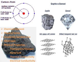
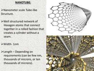
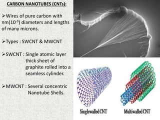

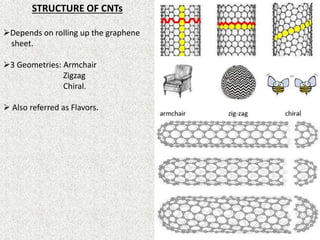
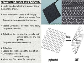
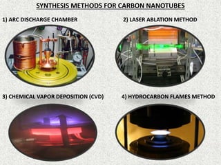
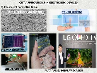
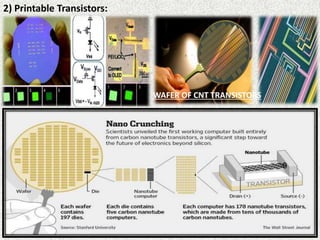
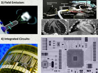
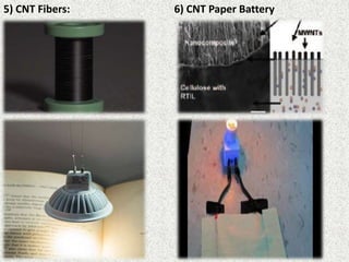
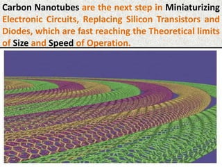


This document discusses carbon nanotubes, their properties, synthesis, and applications in electronic devices. It describes that carbon nanotubes are cylindrical structures made of rolled graphene sheets that are only a few nanometers in width but can be many microns in length. They exist as single-walled nanotubes or multi-walled nanotubes. The document outlines different methods for synthesizing carbon nanotubes and reviews their applications, including uses in transparent conductive films, printable transistors, field emission, integrated circuits, fibers, and paper batteries. In conclusion, it states that carbon nanotubes are poised to replace silicon in miniaturizing electronic circuits and pushing beyond the theoretical limits of silicon transistors.


