Downloaded 133 times
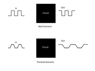

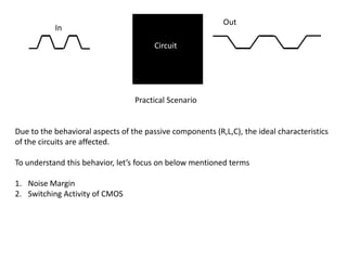
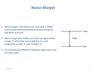
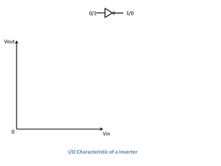
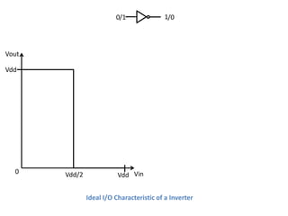
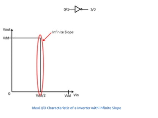
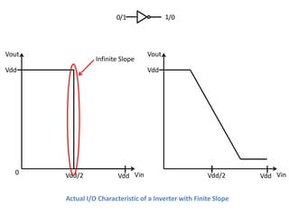
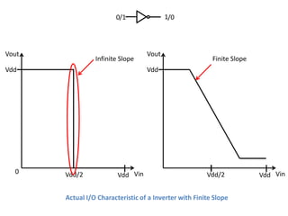
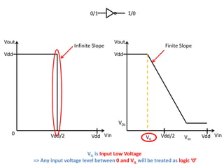
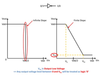
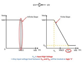
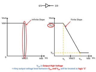
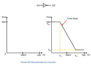
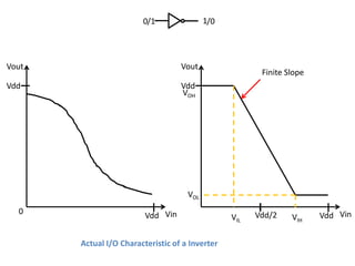
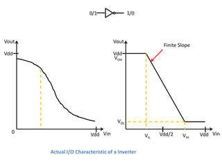
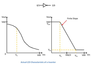

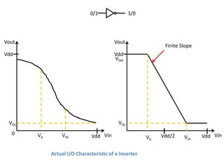
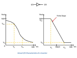
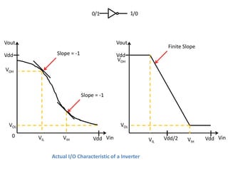
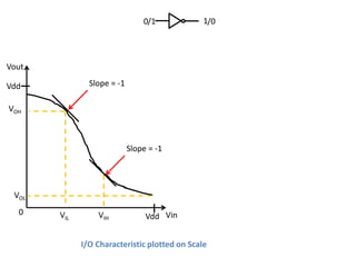
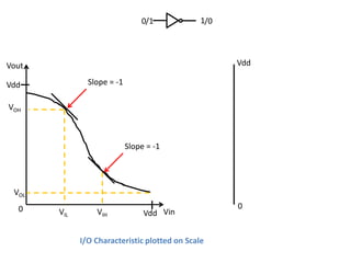
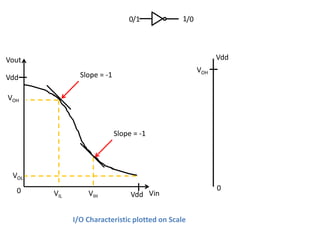

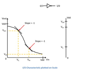

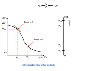
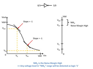
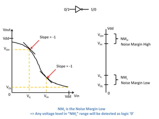
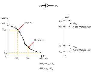
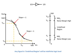
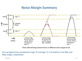

The document discusses the impact of passive components in CMOS circuits, focusing on noise margin and switching activity. It explains noise margin as the tolerance to noise without altering logic levels, characterizing ideal versus practical input/output behavior of an inverter. Key parameters include input/output high and low voltages, and the importance of defined noise margin ranges for accurate signal recognition.