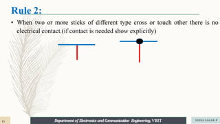
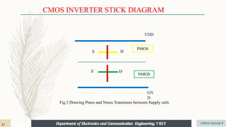
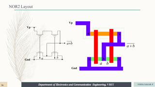
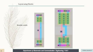
Department of Electronics and Communication Engineering, VBIT
U N I T - 2
VLSI CIRCUIT DESIGN
PROCESSES
P.VIDYA SAGAR ( ASSOCIATE PROFESSOR)
VLSI
SYLLABUS
UNIT II
VLSI CIRCUIT DESIGN PROCESSES: VLSI Design Flow, MOS Layers, Stick Diagrams, Design
Rules and Layout, 2 m CMOS Design rules for wires, Contacts and Transistors Layout Diagrams for
NMOS and CMOS Inverters and Gates, Scaling of MOS circuits.
Department of Electronics and Communication Engineering, VBIT
Department of Electronics and Communication Engineering, VBIT VIDYA SAGAR P
2
CONTENTS:
➢ VLSI design flow
➢ MOS layers
➢ Stick Diagrams
➢ Design Rules and Layout diagrams
➢ 2µm Design Rules
➢ Layout Diagrams for Inverter, Logic gates
➢ Scaling of MOS
Department of Electronics and Communication Engineering, VBIT
Department of Electronics and Communication Engineering, VBIT VIDYA SAGAR P
3
➢VLSI design flow
Department of Electronics and Communication Engineering, VBIT
Department of Electronics and Communication Engineering, VBIT VIDYA SAGAR P
4
Department of Electronics and Communication Engineering, VBIT
Department of Electronics and Communication Engineering, VBIT VIDYA SAGAR P
5
MOS Layers :
There are 4 layers
• N-diffusion
• P-diffusion
• Poly Si
• Metal
•These layers are isolated by one another by thick or thin silicon dioxide insulating layers.
• Thin oxide mask region includes n-diffusion / p-diffusion and transistor channel.
Department of Electronics and Communication Engineering, VBIT
Department of Electronics and Communication Engineering, VBIT VIDYA SAGAR P
6
Stick Diagrams :
➢ Astick diagram is a cartoon of a layout.
➢Does show all components/ vias (except possibly tub ties), relative
placement.
➢Does not show exact placement, transistor sizes, wire lengths, wire
widths, tub boundaries
Department of Electronics and Communication Engineering, VBIT
Department of Electronics and Communication Engineering, VBIT VIDYA SAGAR P
7
• Key idea: "Stick figure cartoon" of a layout
• Useful for planning layout
 relative placement of transistors
 assignment of signals to layers
 connections between cells
 cell hierarchy
Department of Electronics and Communication Engineering, VBIT
Department of Electronics and Communication Engineering, VBIT VIDYA SAGAR P
8
Stick Diagrams
Metal
poly
ndiff
pdiff
Can also draw in shades
of gray/line style.
Department of Electronics and Communication Engineering, VBIT VIDYA SAGAR P
9
Rules for Drawing Stick Diagrams :
• Metal 1
• Poly Si
• N-diffusion
• P-diffusion
Rule 1:
• When two or more sticks of the same type cross or touch other that
represents electrical contact.
Department of Electronics and Communication Engineering, VBIT
Department of Electronics and Communication Engineering, VBIT VIDYA SAGAR P
10
Rule 2:
• When two or more sticks of different type cross or touch other there is no
electrical contact.(if contact is needed show explicitly)
Department of Electronics and Communication Engineering, VBIT
Department of Electronics and Communication Engineering, VBIT VIDYA SAGAR P
11
Rule 3: When a poly crosses diffusion it represents MOSFET. If contact is
shown it is not transistor.
nMOSFET pMOSFET nMOSFET
(Depletion Mode)
Department of Electronics and Communication Engineering, VBIT
Department of Electronics and Communication Engineering, VBIT VIDYA SAGAR P
12
STICK DIAGRAMS
PMOS Enhancement Transistor
NMOS Enhancement Transistor
NMOS Depletion transistor
NPN Bipolar Transistor
P- Diffusion
n- Diffusion
Poly silicon
Metal 1
Contact cut
N implant
Demarcation line
Substrate contact
Buried Contact
Department of Electronics and Communication Engineering, VBIT
Department of Electronics and Communication Engineering, VBIT VIDYA SAGAR P
13
Stick diagram
Encodings for a simple single metal nMOS process
COLOR STICK ENCODING
MONOCROME
LAYERS MASK LAYOUT ENCODING
MONOCROME
CIF LAYER
Caltech
Intermediate Form
GREEN
RED
BLUE
BLACK
GRAY
nMOS
ONLY
YELLOW
nMOS ONLY
BROWN
NOT APPLICABLE
n-diffusion
n+active
Thniox
Polysilicon
Metal 1
Contact cut
Overglass
Implant
Buried
contact
ND
NP
NM
NC
NG
NI
NB
Department of Electronics and Communication Engineering, VBIT VIDYA SAGAR P
14
nMOS Design Style:
Step 1:Draw metal VDD and GND rails in parallel leaving sufficient space for
circuit components between them.
VDD
GND
Step 2: Thinox (green) paths are drawn between rails for inverter &
inverter logic.
Vin
VOUT
VDD
GND
Department of Electronics and Communication Engineering, VBIT
Department of Electronics and Communication Engineering, VBIT VIDYA SAGAR P
15
Step 3: Connect poly over thinox wherever transistor required.
Department of Electronics and Communication Engineering, VBIT
Department of Electronics and Communication Engineering, VBIT VIDYA SAGAR P
16
Step 4: Connect metal wherever is required and create contact for connection.
Vout
Vin
Vin
VOUT
VDD
GND
Depletion
mode nMOS
Department of Electronics and Communication Engineering, VBIT
Department of Electronics and Communication Engineering, VBIT VIDYA SAGAR P
17
GND
NMOS INVERTER STICK DIAGRAM
D
A
B
S
VDD
D
5 V
Department of Electronics and Communication Engineering, VBIT
Department of Electronics and Communication Engineering, VBIT VIDYA SAGAR P
18
Dep
Vout
Enh
0V
5 V
Dep
Vout
Enh
0V
0 V
V
V
i
i
n
n
5 v
Department of Electronics and Communication Engineering, VBIT VIDYA SAGAR P
19
VDD
CMOS INVERTER STICK DIAGRAM
GND
FIG 1 Supply rails
Department of Electronics and Communication Engineering, VBIT
Department of Electronics and Communication Engineering, VBIT VIDYA SAGAR P
20
VDD
PMOS
NMOS
S
S
D
D
CMOS INVERTER STICK DIAGRAM
GN
D
Fig 2 Drawing Pmos and Nmos Transistors between Supply rails
Department of Electronics and Communication Engineering, VBIT
Department of Electronics and Communication Engineering, VBIT VIDYA SAGAR P
21
VDD
PMOS
NMOS
A
S
S
D
D
CMOS INVERTER STICK DIAGRAM
GND
Fig 3 Combining Gate of Pmos and Nmos Transistors and giving common input With same gate poly silicon metal
Department of Electronics and Communication Engineering, VBIT
Department of Electronics and Communication Engineering, VBIT VIDYA SAGAR P
22
VDD
PMOS
NMOS
A
D
S
S D
CMOS INVERTER STICK DIAGRAM
GND
Fig 4 Combining Drain pf Pmos and Nmos Transistors to take output with metal 1
Department of Electronics and Communication Engineering, VBIT
Department of Electronics and Communication Engineering, VBIT VIDYA SAGAR P
23
VDD
PMOS
NMOS
D
A
S
S D
B
CMOS INVERTER STICK DIAGRAM
GND
Fig 5 Take the output with the poly silicon metal
Department of Electronics and Communication Engineering, VBIT
Department of Electronics and Communication Engineering, VBIT VIDYA SAGAR P
24
VDD
PMOS
NMOS
D
A
S
S D
B
CMOS INVERTER STICK DIAGRAM
GND
Fig 6 Connect the source of Pmos to VDD and Nmos to GND
Department of Electronics and Communication Engineering, VBIT
Department of Electronics and Communication Engineering, VBIT VIDYA SAGAR P
25
VDD
PMOS
NMOS
D
A
S
S D
B
CONTACT
CMOS INVERTER STICK DIAGRAM
GND
Fig 7 Connect the contact cuts where the different metals are connected
Department of Electronics and Communication Engineering, VBIT
Department of Electronics and Communication Engineering, VBIT VIDYA SAGAR P
26
VDD
GND
PMOS
NMOS
D
A
S
S D
B
CONTACT
CMOS INVERTER STICK DIAGRAM
Fig 8 Final CMOS Inverter
Substrate contact
Department of Electronics and Communication Engineering, VBIT
Department of Electronics and Communication Engineering, VBIT VIDYA SAGAR P
27
Alternate Layout of NOT Gate
Gnd
Vp
x
x
X
x
Vp
Gnd
X
x
X
X
Department of Electronics and Communication Engineering, VBIT VIDYA SAGAR P
28
NAND GATE
Schematic Stick diagram Layout
Department of Electronics and Communication Engineering, VBIT VIDYA SAGAR P
29
VDD
CMOS NAND GATE STICK DIAGRAM
GND
FIG 9 Supply rails
Department of Electronics and Communication Engineering, VBIT
Department of Electronics and Communication Engineering, VBIT VIDYA SAGAR P
30
VDD
CMOS NAND GATE STICK DIAGRAM
GND
Fig 10 Drawing P and N Diffusion between Supply rails
Department of Electronics and Communication Engineering, VBIT
Department of Electronics and Communication Engineering, VBIT VIDYA SAGAR P
31
VDD
S
S
S D
D D
D S
A B
C
CMOS NAND GATE STICK DIAGRAM
GND
Fig 11 Drawing the poly silicon for two different inputs and
identify the source and drain
Department of Electronics and Communication Engineering, VBIT
Department of Electronics and Communication Engineering, VBIT VIDYA SAGAR P
32
VDD
S
S
S
D D
D
D S
A B
C
CMOS NAND GATE STICK DIAGRAM
GND
Fig 12 Connect the source of Pmos to VDD and Nmos to GND and
subtrate contacts of both
Department of Electronics and Communication Engineering, VBIT
Department of Electronics and Communication Engineering, VBIT VIDYA SAGAR P
33
VDD
S
S
S
D D
D
D S
A B
C
CMOS NAND GATE STICK DIAGRAM
GND
Fig 13 Draw the output connections
Department of Electronics and Communication Engineering, VBIT
Department of Electronics and Communication Engineering, VBIT VIDYA SAGAR P
34
VDD
S
S
S
D
D D
D
S
A B
C
CMOS NAND GATE STICK DIAGRAM
GND
Fig 14 Connect the contact cuts where the different metals are connected
Gnd
Vp
a .b
Department of Electronics and Communication Engineering, VBIT
Department of Electronics and Communication Engineering, VBIT VIDYA SAGAR P
35
a b
Department of Electronics and Communication Engineering, VBIT
36
Vdd CONTACT
VSS CONTACT
Vdd
VSS
DEMARCATION LINE
VOUT(A NAND B)
A
PLOY(G)
PLOY(G)
PLOY(G)
S
PLOY(G)
S S
D
D
S
D
D
B
Cmos Nor GATE
VIDYA SAGAR P
Cmos Nor GATE
Department of Electronics and Communication Engineering, VBIT VIDYA SAGAR P
37
Power
Department of Electronics and Communication Engineering, VBIT VIDYA SAGAR P
38
Ground
C
B
Out
A
BiCmos inverter
Vss contact
Department of Electronics and Communication Engineering, VBIT VIDYA SAGAR P
39
Vdd
Vss
Dem
ar cation
Line Vout
Vdd contact
Department of Electronics and Communication Engineering, VBIT
Encodings for NMOS process:
40 VIDYA SAGAR P
Encodings for CMOS process:
•Figure shows when a n-transistor is
formed: a transistor is formed when a
green line (n+ diffusion) crosses a red
line (poly) completely.
•Figure also shows when a p-
transistor is formed: a transistor is
formed when a yellow line(p+
diffusion) crosses a red line (poly)
completely
Department of Electronics and Communication Engineering, VBIT VIDYA SAGAR P
41
Encoding for BJT and MOSFETs:
layers in an nMOS chip consists of
 a p-type substrate
 paths of n-type diffusion
 a thin layer of silicon dioxide
 paths of polycrystalline silicon
 a thick layer of silicon dioxide
 paths of metal (usually aluminium)
 a further thick layer of silicon dioxide
Department of Electronics and Communication Engineering, VBIT VIDYA SAGAR P
42
LAYOUT
Department of Electronics and Communication Engineering, VBIT
Department of Electronics and Communication Engineering, VBIT VIDYA SAGAR P
43
1.Scalable Design Rules (e.g. SCMOS, λ-based design rules):
In this approach, all rules are defined in terms of a single parameter λ.
The rules are so chosen that a design can be easily ported over a cross section of industrial
process ,making the layout portable .Scaling can be easily done by simply changing the
value .
2.Absolute Design Rules (e.g. μ-based design rules ) :
In this approach, the design rules are expressed in absolute dimensions (e.g.0.75μm) and
therefore can exploit the features of a given process to a maximum degree.
There are primarily two approaches in describing the design rules
Department of Electronics and Communication Engineering, VBIT
Department of Electronics and Communication Engineering, VBIT VIDYA SAGAR P
44
What is Via?
It is used to connect higher level metals from metal1 connection
The direct connections between metal, polysilicon, and diffusion use
intermediate layers such as the contact-cut and the buried-contact layers.
The entire chip is typically covered with a layer of protective coating called
overglass
Department of Electronics and Communication Engineering, VBIT
Department of Electronics and Communication Engineering, VBIT VIDYA SAGAR P
45
Buried contacts:
The buried contact is a method to make direct ohmic contact between the polysilicon gate material and
the junctions, in silicon-gate integrated circuits.
With this method – requiring an additional masking layer – it was possible to use the polysilicon as an
additional layer of interconnection, greatly improving the circuit density, particularly in random logic
circuits.
Here gate length is dependent upon the alignment of the buried contact mask relative to the poly silicon
and therefore vary by ± λ.
Butting contact:
The gate and source of a depletion device can be connected by a method known as butting contact.
Here metal makes contact to both the diffusion forming the source of the depletion transistor and to the
poly silicon forming this device’s gate.
Its advantage is that no buried contact mask is required and it avoids associated processing.
Department of Electronics and Communication Engineering, VBIT VIDYA SAGAR P
46
CMOS Process Layers
Polysilicon
Metal1
Metal2
Contact To Poly
Contact To Diffusion
Via
Well (p,n)
ActiveArea (n+,p+)
Layer Color Representation
Yellow
Green
Red
Blue
Magenta
Black
Black
Black
Select (p+,n+) Green
Department of Electronics and Communication Engineering, VBIT VIDYA SAGAR P
47
2λ
2λ
1λ
2λ
3λ
P diffusion N diffusion
P diffusion
P diffusion N diffusion
P diffusion
METAL 1
METAL 1
4λ
4λ
3λ
Department of Electronics and Communication Engineering, VBIT
Department of Electronics and Communication Engineering, VBIT VIDYA SAGAR P
48
Intra-Layer Design Rules
Metal2
4
3
10
9
0
Well
Active
3
3
Polysilicon
2
2
Different Potential
Same Potential
Metal1
3
3
2
Select
2
or
6
2
Contact
or Via
Hole
Department of Electronics and Communication Engineering, VBIT VIDYA SAGAR P
49
Transistor Layout
1
2
5
3
Transistor
Department of Electronics and Communication Engineering, VBIT VIDYA SAGAR P
50
Via’s and Contacts
1
2
1
Via
Metal to
Poly Contact
Metal to
Active Contac t
1
2
5
4
3 2
2
Department of Electronics and Communication Engineering, VBIT VIDYA SAGAR P
51
Select Layer
1
3 3
2
2
2
Well
Substrate
Select
3
5
Department of Electronics and Communication Engineering, VBIT VIDYA SAGAR P
52
2λ
4λ
4λ
1λ 2λ 4λ
4λ
1λ
2λ
3λ
Department of Electronics and Communication Engineering, VBIT
Department of Electronics and Communication Engineering, VBIT VIDYA SAGAR P
53
2λ
2λ
2λ
2λ 2λ
2λ
2λ
2λ
2λ
2λ
6λ x 6λ
2λ
2λ
2λ
2λ
2λ
NMOS
ENHANCEMENT
PMOS
ENHANCEMENT
NMOS
DEPLETION
Department of Electronics and Communication Engineering, VBIT
Department of Electronics and Communication Engineering, VBIT VIDYA SAGAR P
54
LAMBDA BSED RULES
Department of Electronics and Communication Engineering, VBIT
Department of Electronics and Communication Engineering, VBIT VIDYA SAGAR P
55
Department of Electronics and Communication Engineering, VBIT
Department of Electronics and Communication Engineering, VBIT VIDYA SAGAR P
56
Department of Electronics and Communication Engineering, VBIT
Department of Electronics and Communication Engineering, VBIT VIDYA SAGAR P
57
Department of Electronics and Communication Engineering, VBIT
Department of Electronics and Communication Engineering, VBIT VIDYA SAGAR P
58
Department of Electronics and Communication Engineering, VBIT
Department of Electronics and Communication Engineering, VBIT VIDYA SAGAR P
59
Department of Electronics and Communication Engineering, VBIT
Department of Electronics and Communication Engineering, VBIT VIDYA SAGAR P
60
Department of Electronics and Communication Engineering, VBIT
Department of Electronics and Communication Engineering, VBIT VIDYA SAGAR P
61
Department of Electronics and Communication Engineering, VBIT
Department of Electronics and Communication Engineering, VBIT VIDYA SAGAR P
62
Department of Electronics and Communication Engineering, VBIT
Department of Electronics and Communication Engineering, VBIT VIDYA SAGAR P
63
Department of Electronics and Communication Engineering, VBIT
Department of Electronics and Communication Engineering, VBIT VIDYA SAGAR P
64
Lambda based Design Rules:
Design rules include width rules and spacing rules.
Mead and Conway developed a set of simplified scalable λ -based design rules, which
are valid for a range of fabrication technologies.
In these rules, the minimum feature size of a technology is characterized as 2 λ .
 All width and spacing rules are specified in terms of the parameter λ .
Department of Electronics and Communication Engineering, VBIT VIDYA SAGAR P
65
Design rules for the diffusion layers and metal layers
Figure shows the design rule n diffusion, p diffusion, poly, metal1 and metal 2. The n and p
diffusion lines is having a minimum width of 2λ and a minimum spacing of 3λ. Similarly
it shows for other layers.
Department of Electronics and Communication Engineering, VBIT VIDYA SAGAR P
66
Design rules for transistors and gate over hang distance
Figure shows the design rule for the transistor, and it also shows that the poly should extend
for a minimum of 2λ beyond the diffusion boundaries.(gate over hang distance)
Department of Electronics and Communication Engineering, VBIT VIDYA SAGAR P
67
Via
VIA is used to connect higher level metals from metal1 connection.
Figure shows the design rules for
contact cuts and Vias. The design rule
for contact is minimum 2λx2λ and
same is applicable for a Via.
Department of Electronics and Communication Engineering, VBIT VIDYA SAGAR P
68
Buried contact and Butting contact
Buried contact is made down
each layer to be joined
Butting contact
The layers are butted together in such a way
the two contact cuts become contiguous
Department of Electronics and Communication Engineering, VBIT VIDYA SAGAR P
69
CMOS LAMBDA BASED DESIGN RULES:
Figure shows the rules to be followed in CMOS well processes to accommodate both n
and p transistors
Department of Electronics and Communication Engineering, VBIT VIDYA SAGAR P
70
CMOS Inverter Layout
A A
’
n
p-substrate Field
Oxide
p+
n+
In
Department of Electronics and Communication Engineering, VBIT
Department of Electronics and Communication Engineering, VBIT VIDYA SAGAR P
71
GND VDD
Out
(a) Layout
(b) Cross-Section along A-A’
A A
’
SCHEMATICAND LAYOUT OF BASIC GATES
a) CMOS INVERTER NOT GATE
Schematic Stick diagram Layout
Department of Electronics and Communication Engineering, VBIT VIDYA SAGAR P
72
The CMOS NOT Gate
X
X
X
X
Vp
Gnd
x
Gnd
n-well
Vp
x x
x
Contact Cut
Department of Electronics and Communication Engineering, VBIT VIDYA SAGAR P
73
Alternate Layout of NOT Gate
Gnd
Vp
x
x
X
x
Vp
Gnd
X
x
X
X
Department of Electronics and Communication Engineering, VBIT
Department of Electronics and Communication Engineering, VBIT VIDYA SAGAR P
74
b) NAND GATE
Schematic Stick diagram Layout
Department of Electronics and Communication Engineering, VBIT VIDYA SAGAR P
75
NAND2 Layout
Gnd
Vp
a .b
a b
X
Vp
Gnd
X X
X X
a b
a .b
Department of Electronics and Communication Engineering, VBIT VIDYA SAGAR P
76
Department of Electronics and Communication Engineering, VBIT VIDYA SAGAR P
77
NOR2 Layout
Gnd
Vp
ab
a b
X
Vp
Gnd
X X
X X
a b
a  b
Department of Electronics and Communication Engineering, VBIT VIDYA SAGAR P
78
TRANSMISSION GATE
Symbol schematic stick diagram
layout
Department of Electronics and Communication Engineering, VBIT VIDYA SAGAR P
79
Example: Inverter
Department of Electronics and Communication Engineering, VBIT VIDYA SAGAR P
80
Inverter, contd..
Layout using Electric
Department of Electronics and Communication Engineering, VBIT
Department of Electronics and Communication Engineering, VBIT VIDYA SAGAR P
81
Example: NAND3
•Horizontal N-diffusion and p-diffusion strips
•Vertical polysilicon gates
•Metal1 VDD rail at top
•Metal1 GND rail at bottom
•32 by 40
Department of Electronics and Communication Engineering, VBIT VIDYA SAGAR P
82
NAND3 (using Electric), contd.
Department of Electronics and Communication Engineering, VBIT
Department of Electronics and Communication Engineering, VBIT VIDYA SAGAR P
83
Department of Electronics and Communication Engineering, VBIT
Department of Electronics and Communication Engineering, VBIT VIDYA SAGAR P
84
Scaling
• VLSI technology is constantly evolving towards smaller line widths
• Reduced feature size generally leads to
– better / faster performance
– More gate / chip
• More accurate description of modern technology is ULSI (ultra large
scale integration
Department of Electronics and Communication Engineering, VBIT
Department of Electronics and Communication Engineering, VBIT VIDYA SAGAR P
85
Scaling Factors
• In our discussions we will consider 2 scaling factors, α and β
• 1/ β is the scaling factor for VDD and oxide thickness D
• 1/ α is scaling factor for all other linear dimensions
• We will assume electric field is kept constant
Department of Electronics and Communication Engineering, VBIT
Department of Electronics and Communication Engineering, VBIT VIDYA SAGAR P
86
Scaling Factors for Device Parameters
Simple derivations showing the effects of scaling are derived in Pucknell and Eshraghian pages 125 - 129
It is important that you understand how the following parameters are effected by scaling.
 GateArea
 Gate Capacitance per unit area
 Gate Capacitance
 Charge in Channel
 Channel Resistance
 Transistor Delay
 Maximum Operating Frequency
 Transistor Current
 Switching Energy
 Power Dissipation Per Gate (Static and Dynamic)
 Power Dissipation Per UnitArea
 Power - Speed Product
Department of Electronics and Communication Engineering, VBIT
Department of Electronics and Communication Engineering, VBIT VIDYA SAGAR P
87
MOSFET Scaling
❑ Constant Field Scaling
❑ Constant Voltage Scaling
❑ Lateral Scaling
❑SCALING - refers to ordered reduction in dimensions of the MOSFET and other VLSI features
❑Reduce Size of VLSI chips.
❑Change operational characteristics of MOSFETs and parasitic.
❑Physical limits restrict degree of scaling that can be achieved.
Department of Electronics and Communication Engineering, VBIT
Department of Electronics and Communication Engineering, VBIT VIDYA SAGAR P
88
Constant Field Scaling
❑ The electric field E is kept constant, and the scaled device is obtained by applying a dimensionless scale-
factor α (such that E is unchanged):
❑ all dimensions, including those vertical to the surface (1/α)
❑ device voltages (1/α)
❑ the concentration densities (α).
Department of Electronics and Communication Engineering, VBIT
Department of Electronics and Communication Engineering, VBIT VIDYA SAGAR P
89
Constant Voltage Scaling
❑ Vdd is kept constant.
❑ All dimensions, including those vertical to the surface are scaled.
❑ Concentration densities are scaled.
Department of Electronics and Communication Engineering, VBIT
Department of Electronics and Communication Engineering, VBIT VIDYA SAGAR P
90
Lateral Scaling
❑ Only the gate length is scaled L = 1/α (gate-shrink).
❑ Year Feature Size(μm)
1980 5.0
1983 3.5
1985 2.5
1987 1.75
1989 1.25
1991 1.0
1993 0.8
1995 0.6
Department of Electronics and Communication Engineering, VBIT
Department of Electronics and Communication Engineering, VBIT VIDYA SAGAR P
91
PARAMETER SCALING MODEL
Constant Constant Lateral
Length (L)
Field Voltage
1/α 1/α 1/α
Width (W) 1/α 1/α 1
Supply Voltage (V) 1/α 1 1
Gate Oxide thickness (tox) 1/α 1/α 1
Junction depth (Xj) 1/α 1/α 1
Current (I) 1/α α α
Power Dissipation (P) 1/α2 α α
Electric Field 1 α 1
Load Capacitance (C)
Gate Delay (T)
1/α 1/α
1/α 1/α2
1/α
1/α2
Department of Electronics and Communication Engineering, VBIT
Department of Electronics and Communication Engineering, VBIT VIDYA SAGAR P
92
Scaling of Interconnects
• Resistance of track R ~ L / wt
• R (scaled) ~ (L / α) / ( (w/ α )* (t
/α))
• R(scaled) = αR
• therefore resistance increases with
scaling
t w L
A
B
Department of Electronics and Communication Engineering, VBIT
Department of Electronics and Communication Engineering, VBIT VIDYA SAGAR P
93
Scaling - Time Constant
• Time constant of track connected to gate,
• T = R * Cg
• T(scaled) = α R * (β / α2) *Cg = (β / α) *R*Cg
• Let β = α, therefore T is unscaled!
• Therefore delays in tracks don’t reduce with scaling
• Therefore as tracks get proportionately larger, effect gets worse
• Cross talk between connections gets worse because of reduced spacing
Department of Electronics and Communication Engineering, VBIT
Department of Electronics and Communication Engineering, VBIT VIDYA SAGAR P
94
Scaling of MOS and circuit parameter
Department of Electronics and Communication Engineering, VBIT
Department of Electronics and Communication Engineering, VBIT VIDYA SAGAR P
95
Department of Electronics and Communication Engineering, VBIT VIDYA SAGAR P
96

vlsi-unit-3-ppt.pptx

  • 1.
    Department of Electronicsand Communication Engineering, VBIT Department of Electronics and Communication Engineering, VBIT U N I T - 2 VLSI CIRCUIT DESIGN PROCESSES P.VIDYA SAGAR ( ASSOCIATE PROFESSOR) VLSI
  • 2.
    SYLLABUS UNIT II VLSI CIRCUITDESIGN PROCESSES: VLSI Design Flow, MOS Layers, Stick Diagrams, Design Rules and Layout, 2 m CMOS Design rules for wires, Contacts and Transistors Layout Diagrams for NMOS and CMOS Inverters and Gates, Scaling of MOS circuits. Department of Electronics and Communication Engineering, VBIT Department of Electronics and Communication Engineering, VBIT VIDYA SAGAR P 2
  • 3.
    CONTENTS: ➢ VLSI designflow ➢ MOS layers ➢ Stick Diagrams ➢ Design Rules and Layout diagrams ➢ 2µm Design Rules ➢ Layout Diagrams for Inverter, Logic gates ➢ Scaling of MOS Department of Electronics and Communication Engineering, VBIT Department of Electronics and Communication Engineering, VBIT VIDYA SAGAR P 3
  • 4.
    ➢VLSI design flow Departmentof Electronics and Communication Engineering, VBIT Department of Electronics and Communication Engineering, VBIT VIDYA SAGAR P 4
  • 5.
    Department of Electronicsand Communication Engineering, VBIT Department of Electronics and Communication Engineering, VBIT VIDYA SAGAR P 5
  • 6.
    MOS Layers : Thereare 4 layers • N-diffusion • P-diffusion • Poly Si • Metal •These layers are isolated by one another by thick or thin silicon dioxide insulating layers. • Thin oxide mask region includes n-diffusion / p-diffusion and transistor channel. Department of Electronics and Communication Engineering, VBIT Department of Electronics and Communication Engineering, VBIT VIDYA SAGAR P 6
  • 7.
    Stick Diagrams : ➢Astick diagram is a cartoon of a layout. ➢Does show all components/ vias (except possibly tub ties), relative placement. ➢Does not show exact placement, transistor sizes, wire lengths, wire widths, tub boundaries Department of Electronics and Communication Engineering, VBIT Department of Electronics and Communication Engineering, VBIT VIDYA SAGAR P 7
  • 8.
    • Key idea:"Stick figure cartoon" of a layout • Useful for planning layout  relative placement of transistors  assignment of signals to layers  connections between cells  cell hierarchy Department of Electronics and Communication Engineering, VBIT Department of Electronics and Communication Engineering, VBIT VIDYA SAGAR P 8
  • 9.
    Stick Diagrams Metal poly ndiff pdiff Can alsodraw in shades of gray/line style. Department of Electronics and Communication Engineering, VBIT VIDYA SAGAR P 9
  • 10.
    Rules for DrawingStick Diagrams : • Metal 1 • Poly Si • N-diffusion • P-diffusion Rule 1: • When two or more sticks of the same type cross or touch other that represents electrical contact. Department of Electronics and Communication Engineering, VBIT Department of Electronics and Communication Engineering, VBIT VIDYA SAGAR P 10
  • 11.
    Rule 2: • Whentwo or more sticks of different type cross or touch other there is no electrical contact.(if contact is needed show explicitly) Department of Electronics and Communication Engineering, VBIT Department of Electronics and Communication Engineering, VBIT VIDYA SAGAR P 11
  • 12.
    Rule 3: Whena poly crosses diffusion it represents MOSFET. If contact is shown it is not transistor. nMOSFET pMOSFET nMOSFET (Depletion Mode) Department of Electronics and Communication Engineering, VBIT Department of Electronics and Communication Engineering, VBIT VIDYA SAGAR P 12
  • 13.
    STICK DIAGRAMS PMOS EnhancementTransistor NMOS Enhancement Transistor NMOS Depletion transistor NPN Bipolar Transistor P- Diffusion n- Diffusion Poly silicon Metal 1 Contact cut N implant Demarcation line Substrate contact Buried Contact Department of Electronics and Communication Engineering, VBIT Department of Electronics and Communication Engineering, VBIT VIDYA SAGAR P 13
  • 14.
    Stick diagram Encodings fora simple single metal nMOS process COLOR STICK ENCODING MONOCROME LAYERS MASK LAYOUT ENCODING MONOCROME CIF LAYER Caltech Intermediate Form GREEN RED BLUE BLACK GRAY nMOS ONLY YELLOW nMOS ONLY BROWN NOT APPLICABLE n-diffusion n+active Thniox Polysilicon Metal 1 Contact cut Overglass Implant Buried contact ND NP NM NC NG NI NB Department of Electronics and Communication Engineering, VBIT VIDYA SAGAR P 14
  • 15.
    nMOS Design Style: Step1:Draw metal VDD and GND rails in parallel leaving sufficient space for circuit components between them. VDD GND Step 2: Thinox (green) paths are drawn between rails for inverter & inverter logic. Vin VOUT VDD GND Department of Electronics and Communication Engineering, VBIT Department of Electronics and Communication Engineering, VBIT VIDYA SAGAR P 15
  • 16.
    Step 3: Connectpoly over thinox wherever transistor required. Department of Electronics and Communication Engineering, VBIT Department of Electronics and Communication Engineering, VBIT VIDYA SAGAR P 16
  • 17.
    Step 4: Connectmetal wherever is required and create contact for connection. Vout Vin Vin VOUT VDD GND Depletion mode nMOS Department of Electronics and Communication Engineering, VBIT Department of Electronics and Communication Engineering, VBIT VIDYA SAGAR P 17
  • 18.
    GND NMOS INVERTER STICKDIAGRAM D A B S VDD D 5 V Department of Electronics and Communication Engineering, VBIT Department of Electronics and Communication Engineering, VBIT VIDYA SAGAR P 18 Dep Vout Enh 0V
  • 19.
    5 V Dep Vout Enh 0V 0 V V V i i n n 5v Department of Electronics and Communication Engineering, VBIT VIDYA SAGAR P 19
  • 20.
    VDD CMOS INVERTER STICKDIAGRAM GND FIG 1 Supply rails Department of Electronics and Communication Engineering, VBIT Department of Electronics and Communication Engineering, VBIT VIDYA SAGAR P 20
  • 21.
    VDD PMOS NMOS S S D D CMOS INVERTER STICKDIAGRAM GN D Fig 2 Drawing Pmos and Nmos Transistors between Supply rails Department of Electronics and Communication Engineering, VBIT Department of Electronics and Communication Engineering, VBIT VIDYA SAGAR P 21
  • 22.
    VDD PMOS NMOS A S S D D CMOS INVERTER STICKDIAGRAM GND Fig 3 Combining Gate of Pmos and Nmos Transistors and giving common input With same gate poly silicon metal Department of Electronics and Communication Engineering, VBIT Department of Electronics and Communication Engineering, VBIT VIDYA SAGAR P 22
  • 23.
    VDD PMOS NMOS A D S S D CMOS INVERTERSTICK DIAGRAM GND Fig 4 Combining Drain pf Pmos and Nmos Transistors to take output with metal 1 Department of Electronics and Communication Engineering, VBIT Department of Electronics and Communication Engineering, VBIT VIDYA SAGAR P 23
  • 24.
    VDD PMOS NMOS D A S S D B CMOS INVERTERSTICK DIAGRAM GND Fig 5 Take the output with the poly silicon metal Department of Electronics and Communication Engineering, VBIT Department of Electronics and Communication Engineering, VBIT VIDYA SAGAR P 24
  • 25.
    VDD PMOS NMOS D A S S D B CMOS INVERTERSTICK DIAGRAM GND Fig 6 Connect the source of Pmos to VDD and Nmos to GND Department of Electronics and Communication Engineering, VBIT Department of Electronics and Communication Engineering, VBIT VIDYA SAGAR P 25
  • 26.
    VDD PMOS NMOS D A S S D B CONTACT CMOS INVERTERSTICK DIAGRAM GND Fig 7 Connect the contact cuts where the different metals are connected Department of Electronics and Communication Engineering, VBIT Department of Electronics and Communication Engineering, VBIT VIDYA SAGAR P 26
  • 27.
    VDD GND PMOS NMOS D A S S D B CONTACT CMOS INVERTERSTICK DIAGRAM Fig 8 Final CMOS Inverter Substrate contact Department of Electronics and Communication Engineering, VBIT Department of Electronics and Communication Engineering, VBIT VIDYA SAGAR P 27
  • 28.
    Alternate Layout ofNOT Gate Gnd Vp x x X x Vp Gnd X x X X Department of Electronics and Communication Engineering, VBIT VIDYA SAGAR P 28
  • 29.
    NAND GATE Schematic Stickdiagram Layout Department of Electronics and Communication Engineering, VBIT VIDYA SAGAR P 29
  • 30.
    VDD CMOS NAND GATESTICK DIAGRAM GND FIG 9 Supply rails Department of Electronics and Communication Engineering, VBIT Department of Electronics and Communication Engineering, VBIT VIDYA SAGAR P 30
  • 31.
    VDD CMOS NAND GATESTICK DIAGRAM GND Fig 10 Drawing P and N Diffusion between Supply rails Department of Electronics and Communication Engineering, VBIT Department of Electronics and Communication Engineering, VBIT VIDYA SAGAR P 31
  • 32.
    VDD S S S D D D DS A B C CMOS NAND GATE STICK DIAGRAM GND Fig 11 Drawing the poly silicon for two different inputs and identify the source and drain Department of Electronics and Communication Engineering, VBIT Department of Electronics and Communication Engineering, VBIT VIDYA SAGAR P 32
  • 33.
    VDD S S S D D D D S AB C CMOS NAND GATE STICK DIAGRAM GND Fig 12 Connect the source of Pmos to VDD and Nmos to GND and subtrate contacts of both Department of Electronics and Communication Engineering, VBIT Department of Electronics and Communication Engineering, VBIT VIDYA SAGAR P 33
  • 34.
    VDD S S S D D D D S AB C CMOS NAND GATE STICK DIAGRAM GND Fig 13 Draw the output connections Department of Electronics and Communication Engineering, VBIT Department of Electronics and Communication Engineering, VBIT VIDYA SAGAR P 34
  • 35.
    VDD S S S D D D D S A B C CMOSNAND GATE STICK DIAGRAM GND Fig 14 Connect the contact cuts where the different metals are connected Gnd Vp a .b Department of Electronics and Communication Engineering, VBIT Department of Electronics and Communication Engineering, VBIT VIDYA SAGAR P 35 a b
  • 36.
    Department of Electronicsand Communication Engineering, VBIT Department of Electronics and Communication Engineering, VBIT 36 Vdd CONTACT VSS CONTACT Vdd VSS DEMARCATION LINE VOUT(A NAND B) A PLOY(G) PLOY(G) PLOY(G) S PLOY(G) S S D D S D D B Cmos Nor GATE VIDYA SAGAR P
  • 37.
    Cmos Nor GATE Departmentof Electronics and Communication Engineering, VBIT VIDYA SAGAR P 37
  • 38.
    Power Department of Electronicsand Communication Engineering, VBIT VIDYA SAGAR P 38 Ground C B Out A
  • 39.
    BiCmos inverter Vss contact Departmentof Electronics and Communication Engineering, VBIT VIDYA SAGAR P 39 Vdd Vss Dem ar cation Line Vout Vdd contact
  • 40.
    Department of Electronicsand Communication Engineering, VBIT Department of Electronics and Communication Engineering, VBIT Encodings for NMOS process: 40 VIDYA SAGAR P
  • 41.
    Encodings for CMOSprocess: •Figure shows when a n-transistor is formed: a transistor is formed when a green line (n+ diffusion) crosses a red line (poly) completely. •Figure also shows when a p- transistor is formed: a transistor is formed when a yellow line(p+ diffusion) crosses a red line (poly) completely Department of Electronics and Communication Engineering, VBIT VIDYA SAGAR P 41
  • 42.
    Encoding for BJTand MOSFETs: layers in an nMOS chip consists of  a p-type substrate  paths of n-type diffusion  a thin layer of silicon dioxide  paths of polycrystalline silicon  a thick layer of silicon dioxide  paths of metal (usually aluminium)  a further thick layer of silicon dioxide Department of Electronics and Communication Engineering, VBIT VIDYA SAGAR P 42
  • 43.
    LAYOUT Department of Electronicsand Communication Engineering, VBIT Department of Electronics and Communication Engineering, VBIT VIDYA SAGAR P 43
  • 44.
    1.Scalable Design Rules(e.g. SCMOS, λ-based design rules): In this approach, all rules are defined in terms of a single parameter λ. The rules are so chosen that a design can be easily ported over a cross section of industrial process ,making the layout portable .Scaling can be easily done by simply changing the value . 2.Absolute Design Rules (e.g. μ-based design rules ) : In this approach, the design rules are expressed in absolute dimensions (e.g.0.75μm) and therefore can exploit the features of a given process to a maximum degree. There are primarily two approaches in describing the design rules Department of Electronics and Communication Engineering, VBIT Department of Electronics and Communication Engineering, VBIT VIDYA SAGAR P 44
  • 45.
    What is Via? Itis used to connect higher level metals from metal1 connection The direct connections between metal, polysilicon, and diffusion use intermediate layers such as the contact-cut and the buried-contact layers. The entire chip is typically covered with a layer of protective coating called overglass Department of Electronics and Communication Engineering, VBIT Department of Electronics and Communication Engineering, VBIT VIDYA SAGAR P 45
  • 46.
    Buried contacts: The buriedcontact is a method to make direct ohmic contact between the polysilicon gate material and the junctions, in silicon-gate integrated circuits. With this method – requiring an additional masking layer – it was possible to use the polysilicon as an additional layer of interconnection, greatly improving the circuit density, particularly in random logic circuits. Here gate length is dependent upon the alignment of the buried contact mask relative to the poly silicon and therefore vary by ± λ. Butting contact: The gate and source of a depletion device can be connected by a method known as butting contact. Here metal makes contact to both the diffusion forming the source of the depletion transistor and to the poly silicon forming this device’s gate. Its advantage is that no buried contact mask is required and it avoids associated processing. Department of Electronics and Communication Engineering, VBIT VIDYA SAGAR P 46
  • 47.
    CMOS Process Layers Polysilicon Metal1 Metal2 ContactTo Poly Contact To Diffusion Via Well (p,n) ActiveArea (n+,p+) Layer Color Representation Yellow Green Red Blue Magenta Black Black Black Select (p+,n+) Green Department of Electronics and Communication Engineering, VBIT VIDYA SAGAR P 47
  • 48.
    2λ 2λ 1λ 2λ 3λ P diffusion Ndiffusion P diffusion P diffusion N diffusion P diffusion METAL 1 METAL 1 4λ 4λ 3λ Department of Electronics and Communication Engineering, VBIT Department of Electronics and Communication Engineering, VBIT VIDYA SAGAR P 48
  • 49.
    Intra-Layer Design Rules Metal2 4 3 10 9 0 Well Active 3 3 Polysilicon 2 2 DifferentPotential Same Potential Metal1 3 3 2 Select 2 or 6 2 Contact or Via Hole Department of Electronics and Communication Engineering, VBIT VIDYA SAGAR P 49
  • 50.
    Transistor Layout 1 2 5 3 Transistor Department ofElectronics and Communication Engineering, VBIT VIDYA SAGAR P 50
  • 51.
    Via’s and Contacts 1 2 1 Via Metalto Poly Contact Metal to Active Contac t 1 2 5 4 3 2 2 Department of Electronics and Communication Engineering, VBIT VIDYA SAGAR P 51
  • 52.
    Select Layer 1 3 3 2 2 2 Well Substrate Select 3 5 Departmentof Electronics and Communication Engineering, VBIT VIDYA SAGAR P 52
  • 53.
    2λ 4λ 4λ 1λ 2λ 4λ 4λ 1λ 2λ 3λ Departmentof Electronics and Communication Engineering, VBIT Department of Electronics and Communication Engineering, VBIT VIDYA SAGAR P 53
  • 54.
    2λ 2λ 2λ 2λ 2λ 2λ 2λ 2λ 2λ 2λ 6λ x6λ 2λ 2λ 2λ 2λ 2λ NMOS ENHANCEMENT PMOS ENHANCEMENT NMOS DEPLETION Department of Electronics and Communication Engineering, VBIT Department of Electronics and Communication Engineering, VBIT VIDYA SAGAR P 54
  • 55.
    LAMBDA BSED RULES Departmentof Electronics and Communication Engineering, VBIT Department of Electronics and Communication Engineering, VBIT VIDYA SAGAR P 55
  • 56.
    Department of Electronicsand Communication Engineering, VBIT Department of Electronics and Communication Engineering, VBIT VIDYA SAGAR P 56
  • 57.
    Department of Electronicsand Communication Engineering, VBIT Department of Electronics and Communication Engineering, VBIT VIDYA SAGAR P 57
  • 58.
    Department of Electronicsand Communication Engineering, VBIT Department of Electronics and Communication Engineering, VBIT VIDYA SAGAR P 58
  • 59.
    Department of Electronicsand Communication Engineering, VBIT Department of Electronics and Communication Engineering, VBIT VIDYA SAGAR P 59
  • 60.
    Department of Electronicsand Communication Engineering, VBIT Department of Electronics and Communication Engineering, VBIT VIDYA SAGAR P 60
  • 61.
    Department of Electronicsand Communication Engineering, VBIT Department of Electronics and Communication Engineering, VBIT VIDYA SAGAR P 61
  • 62.
    Department of Electronicsand Communication Engineering, VBIT Department of Electronics and Communication Engineering, VBIT VIDYA SAGAR P 62
  • 63.
    Department of Electronicsand Communication Engineering, VBIT Department of Electronics and Communication Engineering, VBIT VIDYA SAGAR P 63
  • 64.
    Department of Electronicsand Communication Engineering, VBIT Department of Electronics and Communication Engineering, VBIT VIDYA SAGAR P 64
  • 65.
    Lambda based DesignRules: Design rules include width rules and spacing rules. Mead and Conway developed a set of simplified scalable λ -based design rules, which are valid for a range of fabrication technologies. In these rules, the minimum feature size of a technology is characterized as 2 λ .  All width and spacing rules are specified in terms of the parameter λ . Department of Electronics and Communication Engineering, VBIT VIDYA SAGAR P 65
  • 66.
    Design rules forthe diffusion layers and metal layers Figure shows the design rule n diffusion, p diffusion, poly, metal1 and metal 2. The n and p diffusion lines is having a minimum width of 2λ and a minimum spacing of 3λ. Similarly it shows for other layers. Department of Electronics and Communication Engineering, VBIT VIDYA SAGAR P 66
  • 67.
    Design rules fortransistors and gate over hang distance Figure shows the design rule for the transistor, and it also shows that the poly should extend for a minimum of 2λ beyond the diffusion boundaries.(gate over hang distance) Department of Electronics and Communication Engineering, VBIT VIDYA SAGAR P 67
  • 68.
    Via VIA is usedto connect higher level metals from metal1 connection. Figure shows the design rules for contact cuts and Vias. The design rule for contact is minimum 2λx2λ and same is applicable for a Via. Department of Electronics and Communication Engineering, VBIT VIDYA SAGAR P 68
  • 69.
    Buried contact andButting contact Buried contact is made down each layer to be joined Butting contact The layers are butted together in such a way the two contact cuts become contiguous Department of Electronics and Communication Engineering, VBIT VIDYA SAGAR P 69
  • 70.
    CMOS LAMBDA BASEDDESIGN RULES: Figure shows the rules to be followed in CMOS well processes to accommodate both n and p transistors Department of Electronics and Communication Engineering, VBIT VIDYA SAGAR P 70
  • 71.
    CMOS Inverter Layout AA ’ n p-substrate Field Oxide p+ n+ In Department of Electronics and Communication Engineering, VBIT Department of Electronics and Communication Engineering, VBIT VIDYA SAGAR P 71 GND VDD Out (a) Layout (b) Cross-Section along A-A’ A A ’
  • 72.
    SCHEMATICAND LAYOUT OFBASIC GATES a) CMOS INVERTER NOT GATE Schematic Stick diagram Layout Department of Electronics and Communication Engineering, VBIT VIDYA SAGAR P 72
  • 73.
    The CMOS NOTGate X X X X Vp Gnd x Gnd n-well Vp x x x Contact Cut Department of Electronics and Communication Engineering, VBIT VIDYA SAGAR P 73
  • 74.
    Alternate Layout ofNOT Gate Gnd Vp x x X x Vp Gnd X x X X Department of Electronics and Communication Engineering, VBIT Department of Electronics and Communication Engineering, VBIT VIDYA SAGAR P 74
  • 75.
    b) NAND GATE SchematicStick diagram Layout Department of Electronics and Communication Engineering, VBIT VIDYA SAGAR P 75
  • 76.
    NAND2 Layout Gnd Vp a .b ab X Vp Gnd X X X X a b a .b Department of Electronics and Communication Engineering, VBIT VIDYA SAGAR P 76
  • 77.
    Department of Electronicsand Communication Engineering, VBIT VIDYA SAGAR P 77
  • 78.
    NOR2 Layout Gnd Vp ab a b X Vp Gnd XX X X a b a  b Department of Electronics and Communication Engineering, VBIT VIDYA SAGAR P 78
  • 79.
    TRANSMISSION GATE Symbol schematicstick diagram layout Department of Electronics and Communication Engineering, VBIT VIDYA SAGAR P 79
  • 80.
    Example: Inverter Department ofElectronics and Communication Engineering, VBIT VIDYA SAGAR P 80
  • 81.
    Inverter, contd.. Layout usingElectric Department of Electronics and Communication Engineering, VBIT Department of Electronics and Communication Engineering, VBIT VIDYA SAGAR P 81
  • 82.
    Example: NAND3 •Horizontal N-diffusionand p-diffusion strips •Vertical polysilicon gates •Metal1 VDD rail at top •Metal1 GND rail at bottom •32 by 40 Department of Electronics and Communication Engineering, VBIT VIDYA SAGAR P 82
  • 83.
    NAND3 (using Electric),contd. Department of Electronics and Communication Engineering, VBIT Department of Electronics and Communication Engineering, VBIT VIDYA SAGAR P 83
  • 84.
    Department of Electronicsand Communication Engineering, VBIT Department of Electronics and Communication Engineering, VBIT VIDYA SAGAR P 84
  • 85.
    Scaling • VLSI technologyis constantly evolving towards smaller line widths • Reduced feature size generally leads to – better / faster performance – More gate / chip • More accurate description of modern technology is ULSI (ultra large scale integration Department of Electronics and Communication Engineering, VBIT Department of Electronics and Communication Engineering, VBIT VIDYA SAGAR P 85
  • 86.
    Scaling Factors • Inour discussions we will consider 2 scaling factors, α and β • 1/ β is the scaling factor for VDD and oxide thickness D • 1/ α is scaling factor for all other linear dimensions • We will assume electric field is kept constant Department of Electronics and Communication Engineering, VBIT Department of Electronics and Communication Engineering, VBIT VIDYA SAGAR P 86
  • 87.
    Scaling Factors forDevice Parameters Simple derivations showing the effects of scaling are derived in Pucknell and Eshraghian pages 125 - 129 It is important that you understand how the following parameters are effected by scaling.  GateArea  Gate Capacitance per unit area  Gate Capacitance  Charge in Channel  Channel Resistance  Transistor Delay  Maximum Operating Frequency  Transistor Current  Switching Energy  Power Dissipation Per Gate (Static and Dynamic)  Power Dissipation Per UnitArea  Power - Speed Product Department of Electronics and Communication Engineering, VBIT Department of Electronics and Communication Engineering, VBIT VIDYA SAGAR P 87
  • 88.
    MOSFET Scaling ❑ ConstantField Scaling ❑ Constant Voltage Scaling ❑ Lateral Scaling ❑SCALING - refers to ordered reduction in dimensions of the MOSFET and other VLSI features ❑Reduce Size of VLSI chips. ❑Change operational characteristics of MOSFETs and parasitic. ❑Physical limits restrict degree of scaling that can be achieved. Department of Electronics and Communication Engineering, VBIT Department of Electronics and Communication Engineering, VBIT VIDYA SAGAR P 88
  • 89.
    Constant Field Scaling ❑The electric field E is kept constant, and the scaled device is obtained by applying a dimensionless scale- factor α (such that E is unchanged): ❑ all dimensions, including those vertical to the surface (1/α) ❑ device voltages (1/α) ❑ the concentration densities (α). Department of Electronics and Communication Engineering, VBIT Department of Electronics and Communication Engineering, VBIT VIDYA SAGAR P 89
  • 90.
    Constant Voltage Scaling ❑Vdd is kept constant. ❑ All dimensions, including those vertical to the surface are scaled. ❑ Concentration densities are scaled. Department of Electronics and Communication Engineering, VBIT Department of Electronics and Communication Engineering, VBIT VIDYA SAGAR P 90
  • 91.
    Lateral Scaling ❑ Onlythe gate length is scaled L = 1/α (gate-shrink). ❑ Year Feature Size(μm) 1980 5.0 1983 3.5 1985 2.5 1987 1.75 1989 1.25 1991 1.0 1993 0.8 1995 0.6 Department of Electronics and Communication Engineering, VBIT Department of Electronics and Communication Engineering, VBIT VIDYA SAGAR P 91
  • 92.
    PARAMETER SCALING MODEL ConstantConstant Lateral Length (L) Field Voltage 1/α 1/α 1/α Width (W) 1/α 1/α 1 Supply Voltage (V) 1/α 1 1 Gate Oxide thickness (tox) 1/α 1/α 1 Junction depth (Xj) 1/α 1/α 1 Current (I) 1/α α α Power Dissipation (P) 1/α2 α α Electric Field 1 α 1 Load Capacitance (C) Gate Delay (T) 1/α 1/α 1/α 1/α2 1/α 1/α2 Department of Electronics and Communication Engineering, VBIT Department of Electronics and Communication Engineering, VBIT VIDYA SAGAR P 92
  • 93.
    Scaling of Interconnects •Resistance of track R ~ L / wt • R (scaled) ~ (L / α) / ( (w/ α )* (t /α)) • R(scaled) = αR • therefore resistance increases with scaling t w L A B Department of Electronics and Communication Engineering, VBIT Department of Electronics and Communication Engineering, VBIT VIDYA SAGAR P 93
  • 94.
    Scaling - TimeConstant • Time constant of track connected to gate, • T = R * Cg • T(scaled) = α R * (β / α2) *Cg = (β / α) *R*Cg • Let β = α, therefore T is unscaled! • Therefore delays in tracks don’t reduce with scaling • Therefore as tracks get proportionately larger, effect gets worse • Cross talk between connections gets worse because of reduced spacing Department of Electronics and Communication Engineering, VBIT Department of Electronics and Communication Engineering, VBIT VIDYA SAGAR P 94
  • 95.
    Scaling of MOSand circuit parameter Department of Electronics and Communication Engineering, VBIT Department of Electronics and Communication Engineering, VBIT VIDYA SAGAR P 95
  • 96.
    Department of Electronicsand Communication Engineering, VBIT VIDYA SAGAR P 96