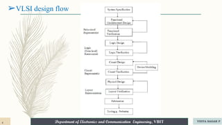
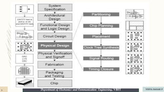
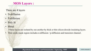
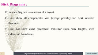
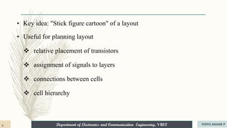
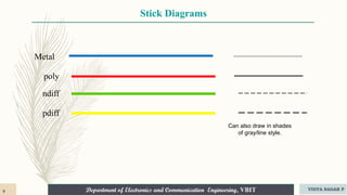
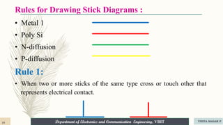
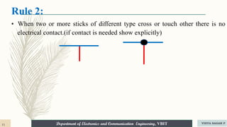
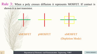
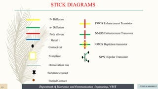
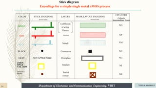
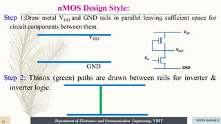
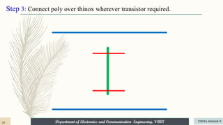
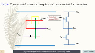
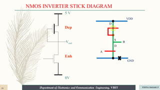
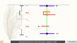
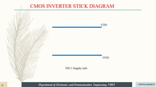
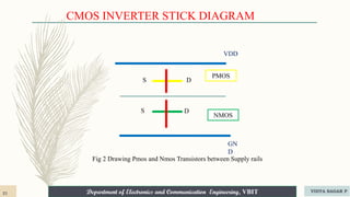
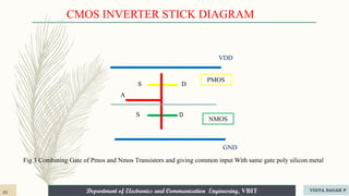
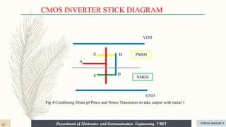
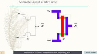
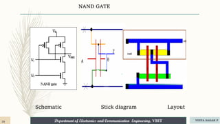
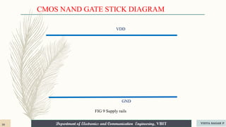
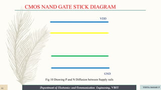
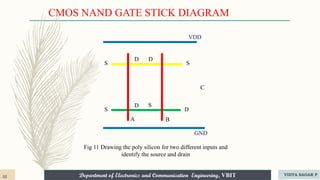
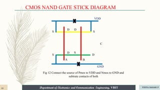
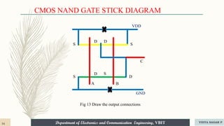
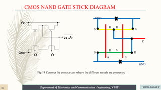
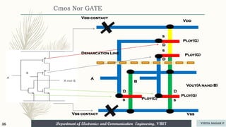
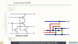
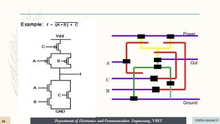
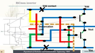
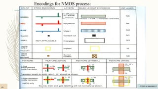
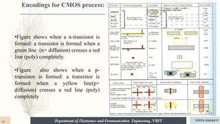
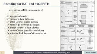
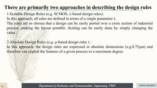
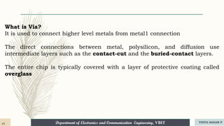
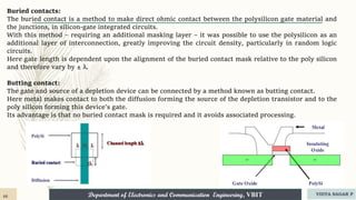
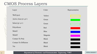
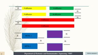
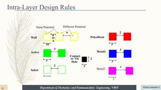
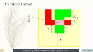
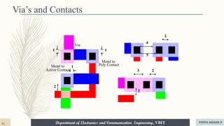
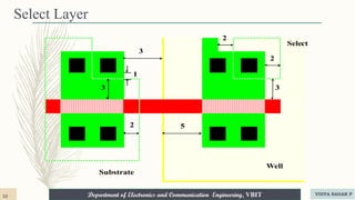
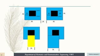
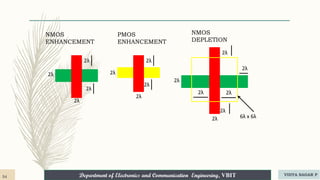
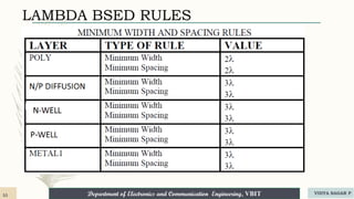
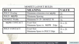
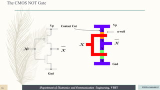
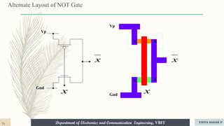
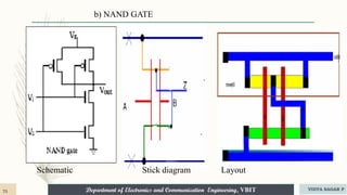
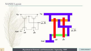
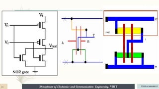
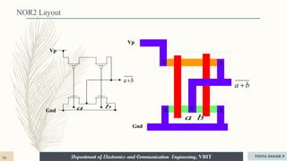
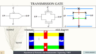
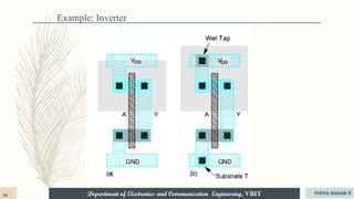
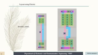
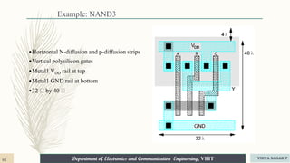
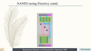
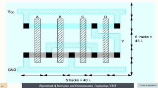
This document contains lecture slides on VLSI circuit design processes from the Department of Electronics and Communication Engineering at VBIT. It discusses topics like VLSI design flow, MOS layers, stick diagrams, design rules, layout diagrams for basic gates like inverters, and scaling of MOS circuits. The document provides illustrations and explanations of concepts like stick diagrams, nMOS and CMOS inverter layout, NAND gate layout, and encodings for representing different layers in VLSI design.